UCC28060-70 AFA
基于UCC28070的交错式功率因数校正电源设计(小项目设计)
基于UCC28070的交错式功率因数校正电源设计UCC28070是先进的功率因素修正器件,集成两个工作在180度反相的交错式PWM,交错工作能降低输入和输出纹波电流,使得导电EMI滤波变得更加容易,成本更低。
利用UCC28070采用BOOST拓扑结构设计了一款功率为1500W的交错式PFC电源。
该系统明显改善乘法器设计,为两个独立的电流放大器提供共享的电流参考,确保匹配的平均电流控制PWM输出模式中都同时保持一个稳定、低失真的正弦输入电流。
可编程工作频率从30 kHz 到300 kHz,有极好的效率和多种保护功能。
与传统控制模式相比,该系统明显增强了PF、效率、总谐波失真等性能。
第1章开关电源1.1 开关电源开关电源是一种电压转换电路,主要的功能是升压和降压,广泛应用于现代电子产品。
广义的说,凡是用半导体器件作为开关,将一种电源形态转变成为另一种电源形态的主电路都叫做开关电源。
电子装置小型轻量化的关键是供电电源的小型化,开关电源具有体积小、效率高等优点,因此在各类电子产品中得到广泛应用。
由于开关电源的控制电路比较复杂。
输出纹波电压较高,所以开关电源的应用受到一定的限制;且开关电源中的调整管工作于开关状态,必然存在开关损耗,而损耗大小随开关频率的提高而增加。
另外,开关电源的变压器、电感等磁性元件及电容的损耗,也随频率的提高而增加,因此,需要尽可能降低电源电路的损耗。
开关电源原理框图如图 1.1所示。
其主电路由防雷单元、输入电磁干扰滤波器(EMI)、输入整流滤波电路、功率变换电路、PWM控制器电路、输出整流滤波电路组成。
辅助电路由功率因数校正电路(PFC)、输入过欠压保护电路、输出过压保护电路、输出限流保护电路、输出短路保护电路等电路构成。
图1.1 开关电源原理框图1.2 开关电源分类开关稳压电源的分类相当复杂,由于看问题的角度不同,分类方法也不同。
有时一个开关稳压电源包含有两种以上的分类办法。
(1)按开关器件进行分类按所选用的开关器件可以分为晶体管开关型、MOSFET管开关型、IGBT管开关型、可控硅开关型、集成电路开关型等数种。
(完整版)UCC28070设计思路
出于应用要求,最近开发了一台基于UCC28070为控制芯片2500W的功率因数校正PFC。
输入电压:85V-265V,输出390V。
PF: 0.9-0.99 ,效率:>96%输出功率最大3400W。
磁环电感采用2个40MM铁硅铝绕制电感量为300uH电感实物图如下:输出电容用了3个330UF的电容,相对来说有点偏小,因为这版设计是配套1500W逆变器后级用在在线式UPS上面,加上逆变桥的电容就能达到要求了。
整机发热方面最严重的还是整流桥堆,目前采用的是2个25A600V的桥堆并联,设计时没想50A的桥堆用到到2500W的时候热量还是挺大的,总体来说整机功率管的热量要小于桥堆。
这是整机的一点不足之处。
需要单独加以小风扇给桥堆散热。
下面是整机工作时的输入电压和输入电流波形:=卜_•■■ ■-' ■■- J;.、❸寡| SAVURETi i r 1.1 i i i i ■ *? i ""~"■ ■ '从图中可以看出电流波形已经基本正弦化,同步于输入电压。
F 图为PFC2个电感的电流波形:这里没有上传细节电感电流展开的波形,实际中 下图为高压直流输出的电流波形: 2电感电流是交错180度的。
SiglentSiiglen tINHI CHI二106mWCH2^ 100UCHI Z0J0&nU「0卜33』M lS.QfiisM PcsjSt@9.0ni£'-冒 SAVETRBC —〒荽型* 图橡储存储存0 = 35.98701<«2OH二500mUCH2- 100UCHI Z0J0&nUW l@.EhsM Pos 5^09.0 ns类型图橡储存从图中可以看出电流为跟随市电电压100HZ的电流波形。
下面是整机的原理图的主要部分。
基于UCC28070-2KW功率因数校正PFC的应用设计整个设计参考TI给出的设计手册:整个设计的开始,定义自己设计的要求:设计内容半3300W单相并联交错功率因素校1EPFC这是卜用f 33O0KWUPSf"jfi[|:野案规格参数十Vin_mjn > 85V Vin_maK > 26弭Vinjtyp ;■ 220VVcut:- .S90Vfp- = 50l-iz fp_min := 47Hz fp_maj( :=PF :- 0.9t| = 0.95Pout ;= 3300Wft = <S3lKHz因为本机没有采用SIC整流二极管,所以频率不能太高。
基于UCC28070的交错式PFC设计
21 0 2年
2 参 数计 算 及选 型
( ) 电路参 数设 计 1主
②检 流 电阻的 计算 与选择
根据 峰值 电流 的 限制 信号 s 主路 电流通 过 电 ,
流互 感器 耦 合 到 检 测 电路 , 在通 过 .s 换 为 电压 R 转 信 号 , 般 留有 1 的 占空 比 调 节余 量 , 电路 轻 一 O 使 载 时不受 影 响. 虑 电阻工 作 时 的额 定功 率 , 择 3 考 选
输 出两路 相 位 相 差 导 通与关 断.
本 更低. 试数据 表明 , 测 与传统 控制模 式相 比 , 系统显
著 增强 了 P 、 率 、 谐波失 真等性 能. F效 总
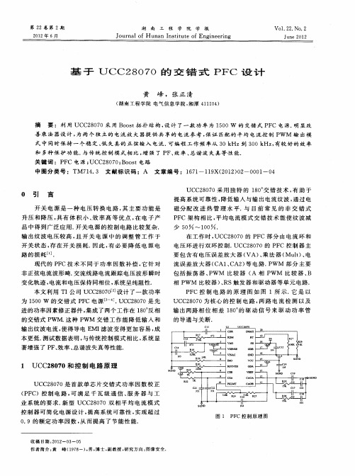
1 UCC 8 7 2 0 0和 控 制 电 路 原 理
开 关状 态 , 存在 开关 损 耗. 因此 , 必 要 降 低 电 源 电 有
路 的 损 耗 . ]
要 包含有 电压误差 放 大器 ( VA) 乘 法器 ( l 、 、 Mut 电 ) 流 误差 放大 器 ( A1 C ) 电路 . WM 部 分 主 要 C 、 A2 等 P 包 括振 荡 器 、 W M 比较 器 ( 相 P P A WM 比较 器 、 B 相 P WM 比较 器 ) R 、 S触 发器 和驱 动器 等单元 电路 . P C控 制 电路 的 原 理 图 如 图 1所 示 . 是 以 F 它 UC 2 0 0为核 心 的控 制 电路 , 路 电流 检 测 以及 C 87 两
UC 2 0 0是首 款单 芯 片交错 式 功 率 因数 校 正 C 87
(F P C)控 制 电 路 , 满 足 千 瓦 级 通 信 、 务 器 与 工 可 服 业 系统 的要 求 . 型 UC 2 0 0双 相平 均 电流 模 式 新 C 87
ucc28063工作原理
ucc28063工作原理ucc28063是一款常用的集成电路芯片,广泛应用于电子设备中。
它具有高性能、低功耗等特点,其工作原理是通过内部的电路结构和功能模块实现的。
ucc28063芯片的工作原理可以简单概括为:输入电压经过整流和滤波后,进入ucc28063芯片,经过内部的开关控制和反馈控制,输出稳定的直流电压。
下面将详细介绍ucc28063芯片的工作原理。
ucc28063芯片的输入电压通常是交流电源,通过整流和滤波电路将其转换为稳定的直流电压。
整流电路使用二极管桥整流,将交流电转换为脉动的直流电,然后通过滤波电容对电压进行平滑,使其变为较为稳定的直流电压。
接下来,稳定的直流电压进入ucc28063芯片,uc28063芯片内部包含多个功能模块,其中包括PWM控制器、反馈控制器、开关驱动器等。
这些功能模块相互配合,实现对输出电压的稳定控制。
PWM控制器是ucc28063芯片的核心模块之一,它通过调节开关的开关时间比例,控制开关管的导通和关断,从而控制输出电压的大小。
具体来说,PWM控制器会根据输出电压与设定的参考电压之间的差值,产生一个控制信号,将其转换为开关管的导通和关断信号。
这样,通过不断调节开关管的导通时间和关断时间,可以使输出电压稳定在设定值附近。
反馈控制器是ucc28063芯片的另一个重要模块,它负责监测输出电压,并将其与设定的参考电压进行比较,得到误差信号。
反馈控制器将误差信号传递给PWM控制器,根据误差信号的大小调整开关管的导通和关断时间,使输出电压趋近于设定值。
ucc28063芯片还包含开关驱动器模块,用于控制开关管的导通和关断。
开关驱动器接收PWM控制器的控制信号,并将其转换为适合开关管工作的高低电平信号,从而实现开关管的导通和关断。
通过上述的工作原理,ucc28063芯片能够实现对输入电压的稳定控制,输出稳定的直流电压。
它在各类电子设备中得到广泛应用,例如电源适配器、电子灯具、电动工具等。
UCC28061中文资料

Natural Interleaving is a trademark of Texas Instuments.
3
PRODUCTION DATA information is current as of publication date. Products conform to specifications per the terms of the Texas Instruments standard warranty. Production processing does not necessarily include testing of all parameters.
ESD damage can range from subtle performance degradation to complete device failure. Precision integrated circuits may be more susceptible to damage because very small parametric changes could cause the device not to meet its published specifications.
PART NUMBER UCC28061D
ORDERING INFORMATION(1)
PACKAGE (2) SOIC 16-Pin (D)
OPERATING TEMPERATURE RANGE, TA –40°C to +125°C
(1) For the most current package and ordering information see the Package Option Addendum at the end of this document, or see the TI web site at .
UCC28070APW;UCC28070APWR;中文规格书,Datasheet资料

UCC28070A SLUSAW0–MARCH2012 Extended Frequency Range(10kHz to300kHz), Interleaving Continuous Conduction Mode PFC ControllerCheck for Samples:UCC28070AFEATURES APPLICATIONS•Interleaved Average Current-Mode PWM•Air Conditioners and White Goods Control with Inherent Current Matching•PFC Applications with IGBT Power Switches •Advanced Current Synthesizer Current•High-Efficiency Server and Desktop Power Sensing for Superior Efficiency Supplies•Highly-Linear Multiplier Output with Internal•Telecom RectifiersQuantized Voltage Feed-Forward Correction•Industrial Equipmentfor Near-Unity PF•Extended Range Programmable Frequency(10DESCRIPTIONkHz to300kHz)The UCC28070A is an extended frequency range •Programmable Maximum Duty-Cycle Clamp derivative of UCC28070,capable of operating at lowswitching frequencies desired for IGBT power switch •Programmable Frequency Dithering Rate andbased PFC converters in high power applications.Magnitude for Enhanced EMI ReductionThe UCC28070A is capable of operating in frequency –Magnitude:3kHz to30kHzrange10kHz to300khz,thus extending the range of –Rate:Up to30kHzoperation compared to UCC28070whose minimum •External Clock Synchronization Capability operating frequency was limited to30khz.All theother features and benefits of UCC28070are also •Enhanced Load and Line Transient Responseavailable in UCC28070A.The180degree out-of-through Voltage Amplifier Output Slew-Ratephase interleaved operation generates substantial Correctionreduction in input and output ripple currents and •Programmable Peak Current Limiting conducted EMI filtering becomes easier and less•Bias-Supply UVLO,Over-Voltage Protection,expensive.Open-Loop Detection,and PFC-EnableMonitoring•External PFC-Disable Interface•Open-Circuit Protection on VSENSE andVINAC pins•Programmable Soft Start•20-Lead TSSOP PackageSimplified Application DiagramPlease be aware that an important notice concerning availability,standard warranty,and use in critical applications ofTexas Instruments semiconductor products and disclaimers thereto appears at the end of this data sheet.PRODUCTION DATA information is current as of publication date.Copyright©2012,Texas Instruments Incorporated Products conform to specifications per the terms of the TexasInstruments standard warranty.Production processing does notnecessarily include testing of all parameters.UCC28070ASLUSAW0– DESCRIPTION(CONT.)Like UCC28070,UCC28070A also features multiple innovations including current synthesis and quantized voltage feed-forward to promote performance enhancements in PF,efficiency,THD,and transient response. Features including frequency dithering,clock synchronization,and slew rate enhancement further expand the potential performance enhancements.All protection features in UCC28070such as output over-voltage detection,programmable peak-current limit,under-voltage lockout and open-loop protection are available in UCC28070A as well.ORDERING INFORMATIONPART NUMBER PACKAGE PACKINGUCC28070APW Plastic,20-Pin TSSOP(PW)70-Pc.TubeUCC28070APWR Plastic,20-Pin TSSOP(PW)2000-Pc.Tape and ReelABSOLUTE MAXIMUM RATINGS(1)(2)(3)(4)over operating free-air temperature range(unless otherwise noted)PARAMETER LIMIT UNIT Supply voltage:VCC22VSupply current:I VCC20mA Voltage:GDA,GDB−0.5to VCC+0.3VGate drive current–continuous:GDA,GDB+/−0.25AGate drive current–pulsed:GDA,GDB+/−0.75Voltage:DMAX,RDM,RT,CDR,VINAC,VSENSE,SS,VAO,IMO,CSA,CSB,−0.5to+7V CAOA,CAOB,PKLMT,VREFCurrent:RT,DMAX,RDM,RSYNTH−0.5mA Current:VREF,VAO,CAOA,CAOB,IMO10Operating junction temperature,T J−40to+125Storage temperature,T STG−65to+150°CLead temperature(10seconds)260(1)These are stress limits.Stress beyond these limits may cause permanent damage to the device.Functional operation of the device atthese or any conditions beyond those indicated under RECOMMENDED OPERATING CONDITIONS is not implied.Exposure to absolute maximum rated conditions for extended periods of time may affect device reliability.(2)All voltages are with respect to GND.(3)All currents are positive into the terminal,negative out of the terminal.(4)In normal use,terminals GDA and GDB are connected to an external gate driver and are internally limited in output current.2Submit Documentation Feedback Copyright©2012,Texas Instruments IncorporatedProduct Folder Link(s):UCC28070AUCC28070A SLUSAW0–MARCH2012ELECTROSTATIC DISCHARGE(ESD)PROTECTIONRATING UNIT Human Body Model(HBM)2,000V Charged Device Model(CDM)500RECOMMENDED OPERATING CONDITIONSover operating free-air temperature range(unless otherwise noted)PARAMETER MIN MAX UNITVCC Input Voltage(from a low-impedance source)V UVLO+1V21VVREF Load Current2mA VINAC Input Voltage Range03IMO Voltage Range0 3.3V PKLMT,CSA,&CSB Voltage Range0 3.6RSYNTH Resistance(R SYN)15750kΩRDM Resistance(R RDM)30330THERMAL INFORMATIONTHERMAL METRIC(1)UNITSPINSθJA Junction-to-ambient thermal resistance(2)θJCtop Junction-to-case(top)thermal resistance(3)θJB Junction-to-board thermal resistance(4)°C/WψJT Junction-to-top characterization parameter(5)ψJB Junction-to-board characterization parameter(6)θJCbot Junction-to-case(bottom)thermal resistance(7)(1)For more information about traditional and new thermal metrics,see the IC Package Thermal Metrics application report,SPRA953.(2)The junction-to-ambient thermal resistance under natural convection is obtained in a simulation on a JEDEC-standard,high-K board,asspecified in JESD51-7,in an environment described in JESD51-2a.(3)The junction-to-case(top)thermal resistance is obtained by simulating a cold plate test on the package top.No specific JEDEC-standard test exists,but a close description can be found in the ANSI SEMI standard G30-88.(4)The junction-to-board thermal resistance is obtained by simulating in an environment with a ring cold plate fixture to control the PCBtemperature,as described in JESD51-8.(5)The junction-to-top characterization parameter,ψJT,estimates the junction temperature of a device in a real system and is extractedfrom the simulation data for obtainingθJA,using a procedure described in JESD51-2a(sections6and7).(6)The junction-to-board characterization parameter,ψJB,estimates the junction temperature of a device in a real system and is extractedfrom the simulation data for obtainingθJA,using a procedure described in JESD51-2a(sections6and7).(7)The junction-to-case(bottom)thermal resistance is obtained by simulating a cold plate test on the exposed(power)pad.No specificJEDEC standard test exists,but a close description can be found in the ANSI SEMI standard G30-88.Copyright©2012,Texas Instruments Incorporated Submit Documentation Feedback3Product Folder Link(s):UCC28070AUCC28070ASLUSAW0–ELECTRICAL CHARACTERISTICSover operating free-air temperature range−40°C<T A<125°C,T J=T A,VCC=12V,GND=0V,R RT=75kΩ,R DMX=68.1kΩ,R RDM=R SYN=100kΩ,C CDR=2.2nF,C SS=C VREF=0.1μF,C VCC=1μF,I VREF=0mA(unless otherwise noted) SYMBOL PARAMETER TEST CONDITIONS MIN TYP MAX UNITS Bias SupplyVCC SHUNT VCC shunt voltage(1)I VCC=10mA232527V VCC current,disabled VSENSE=0V7mA VCC current,enabled VSENSE=3V(switching)912VCC=7V200μA VCC current,UVLOVCC=9V46mAV UVLO UVLO turn-on threshold Measured at VCC(rising)9.810.210.6 UVLO hysteresis Measured at VCC(falling)1VVREF enable threshold Measured at VCC(rising)7.588.5Linear RegulatorVREF voltage,no load I VREF=0mA 5.826 6.18VMeasured as the change in VREF,VREF load rejection-1212(I VREF=0mA and−2mA)mVMeasured as the change in VREF,VREF line rejection-1212(VCC=11V and20V,I VREF=0μA)PFC EnableV EN Enable threshold Measured at VSENSE(rising)0.650.750.85V Enable hysteresis0.15External PFC DisableDisable threshold Measured at SS(falling)0.50.6V Hysteresis VSENSE>0.85V0.15OscillatorOutput phase shift Measured between GDA and GDB179180181DegreeV DMAX,V RT,Timing regulation voltages Measured at DMAX,RT,&RDM 2.913 3.09V and V RDMR RT=750kΩ,R DMX=681kΩ,9.7510.2510.75V RDM=0V,V CDR=6VR RT=75kΩ,R DMX=68.1kΩ,f PWM PWM switching frequency95100105kHzV RDM=0V,V CDR=6VR RT=24.9kΩ,R DMX=22.6kΩ,270290330V RDM=0V,V CDR=6VR RT=75kΩ,R DMX=68.1kΩ,D MAX Duty-cycle clamp92%95%98%V RDM=0V,V CDR=6VR RT=24.9kΩ,R DMX=22.6kΩ,Minimum programmable off-time50150250nsV RDM=0V,V CDR=6VR RDM=316kΩ,R RT=75kΩ234 Frequency dithering magnitude changef DMin f PWM RRDM =31.6kΩ,R RT=24.9kΩ243036kHzC CDR=2.2nF,R RDM=100kΩ3Frequency dithering rate rate off DRchange in f PWM CCDR=0.3nF,R RDM=100kΩ20Dither rate current Measure at CDR(sink and source)±10μAI CDRDither disable threshold Measured at C CDR(rising)5 5.25V (1)Excessive VCC input voltage and/or current damages the device.This clamp will not protect the device from an unregulated supply.Ifan unregulated supply is used,a series-connected fixed positive voltage regulator such as a UA78L15A is recommended.See the Absolute Maximum Ratings section for the limits on VCC voltage and current.4Submit Documentation Feedback Copyright©2012,Texas Instruments IncorporatedProduct Folder Link(s):UCC28070AUCC28070A SLUSAW0–MARCH2012ELECTRICAL CHARACTERISTICS(continued)over operating free-air temperature range−40°C<T A<125°C,T J=T A,VCC=12V,GND=0V,R RT=75kΩ,R DMX=68.1kΩ,R RDM=R SYN=100kΩ,C CDR=2.2nF,C SS=C VREF=0.1μF,C VCC=1μF,I VREF=0mA(unless otherwise noted) SYMBOL PARAMETER TEST CONDITIONS MIN TYP MAX UNITS Clock SynchronizationV CDR SYNC enable threshold Measured at CDR(rising)5 5.25VV CDR=6V,Measured from RDM(rising)toSYNC propagation delay50100nsGDx(rising)SYNC threshold(Rising)V CDR=6V,Measured at RDM 1.2 1.5V SYNC threshold(Falling)V CDR=6V,Measured at RDM0.40.7Positive pulse width0.2μs SYNC pulsesMaximum duty cycle(2)50% Voltage AmplifierVSENSE voltage In regulation,T A=25°C 2.973 3.03V VSENSE voltage In regulation 2.943 3.06VSENSE input bias current In regulation250500nAVAO high voltage VSENSE=2.9V 4.85 5.2V VAO low voltage VSENSE=3.1V0.050.50g MV VAO transconductance 2.8V<VSENSE<3.2V,VAO=3V70μSVAO sink current,overdriven limit VSENSE=3.5V,VAO=3V30VAO source current,overdriven VSENSE=2.5V,VAO=3V,SS=3V−30μA VAO source current,VSENSE=2.5V,VAO=3V−130overdriven limit+I SRCMeasured as VSENSE(falling)/VSENSESlew-rate correction threshold929395%(regulation)Slew-rate correction hysteresis Measured at VSENSE(rising)39mVMeasured at VAO,in addition to VAOI SRC Slew-rate correction current−100μAsource current.Slew-rate correction enable threshold Measured at SS(rising)4VVAO discharge current VSENSE=0.5V,VAO=1V10μA Soft StartI SS SS source current VSENSE=0.9V,SS=1V−10μAAdaptive source current VSENSE=2.0V,SS=1V−1.5-2.5mAAdaptive SS disable Measured as VSENSE–SS-30030mVSS sink current VSENSE=0.5V,SS=0.2V0.50.9mA (2)Due to the influence of the synchronization pulse width on the programmability of the maximum PWM switching duty cycle(D MAX)it isrecommended to minimize the synchronization signal's duty cycle.Copyright©2012,Texas Instruments Incorporated Submit Documentation Feedback5Product Folder Link(s):UCC28070AUCC28070ASLUSAW0–ELECTRICAL CHARACTERISTICS(continued)over operating free-air temperature range−40°C<T A<125°C,T J=T A,VCC=12V,GND=0V,R RT=75kΩ,R DMX=68.1kΩ,R RDM=R SYN=100kΩ,C CDR=2.2nF,C SS=C VREF=0.1μF,C VCC=1μF,I VREF=0mA(unless otherwise noted) SYMBOL PARAMETER TEST CONDITIONS MIN TYP MAX UNITS Over VoltageMeasured as VSENSE(rising)/VSENSEV OVP OVP threshold104106108%(regulation)OVP hysteresis Measured at VSENSE(falling)100mVMeasured between VSENSE(rising)andOVP propagation delay0.20.3μsGDx(falling)Zero-PowerV ZPWR Zero-power detect threshold Measured at VAO(falling)0.650.75V Zero-power hysteresis0.15MultiplierVAO≥1.5V,T A=25°C161718VAO=1.2V,T A=25°C14.517.019.5k MULT Gain constantVAO≥1.5V151719μAVAO=1.2V131721VINAC=0.9V PK,VAO=0.8V-0.200.2I IMO Output current:zeroVINAC=0V,VAO=5V-0.200.2 Quantized Voltage Feed ForwardV LVL1Level1threshold(3)0.60.70.8V LVL2Level2threshold1V LVL3Level3threshold 1.2V LVL4Level4threshold 1.4Measured at VINAC(rising)VV LVL5Level5threshold 1.65V LVL6Level6threshold 1.95V LVL7Level7threshold 2.25V LVL8Level8threshold 2.6Current AmplifiersCAOx high voltage 5.756V CAOx low voltage0.1g MC CAOx transconductance100μSCAOx sink current,overdriven50μA CAOx source current,overdriven−50Input common mode range0 3.6VRSYNTH=6V,T A=25°C-4-8-13 Input offset Voltage mVRSYNTH=6V0-8-20 Input offset voltage0−8−20mVMeasured as Phase A’s input offset minusPhase mismatch-12012Phase B’s input offsetCAOx pull-down current VSENSE=0.5V,CAOx=0.2V0.50.9mA (3)The Level1threshold represents the“zero-crossing detection”threshold above which VINAC must rise to initiate a new input half-cycle,and below which VINAC must fall to terminate that half-cycle.6Submit Documentation Feedback Copyright©2012,Texas Instruments IncorporatedProduct Folder Link(s):UCC28070AUCC28070A SLUSAW0–MARCH2012ELECTRICAL CHARACTERISTICS(continued)over operating free-air temperature range−40°C<T A<125°C,T J=T A,VCC=12V,GND=0V,R RT=75kΩ,R DMX=68.1kΩ,R RDM=R SYN=100kΩ,C CDR=2.2nF,C SS=C VREF=0.1μF,C VCC=1μF,I VREF=0mA(unless otherwise noted) SYMBOL PARAMETER TEST CONDITIONS MIN TYP MAX UNITS Current SynthesizerVSENSE=3V,VINAC=0V 2.913 3.09V RSYNTH Regulation voltageVSENSE=3V,VINAC=2.85V0.100.150.20V Synthesizer disable threshold Measured at RSYNTH(rising)5 5.25VINAC input bias current0.2500.500μA Peak Current LimitPeak current limit threshold PKLMT=3.30V,measured at CSx(rising) 3.27 3.3 3.33VMeasured between CSx(rising)and GDxPeak current limit propagation delay60100ns(falling)edgesPWM RampV RMP PWM ramp amplitude 3.8 4.0 4.2V PWM ramp offset voltage T A=25°C,R RT=75kΩ0.650.7PWM ramp offset temperature−2mV/°C coefficientGate DriveGDA,GDB output voltage,high,VCC=20V,C LOAD=1nF11.51315 clampedV GDA,GDB output voltage,High C LOAD=1nF1010.5GDA,GDB output voltage,Low C LOAD=1nF0.20.3Rise time GDx1V to9V,C LOAD=1nF1830ns Fall time GDx9V to1V,C LOAD=1nF1225GDA,GDB output voltage,UVLO VCC=0V,I GDA,I GDB=2.5mA0.72V Thermal ShutdownThermal shutdown threshold160°C Thermal shutdown recovery140Copyright©2012,Texas Instruments Incorporated Submit Documentation Feedback7Product Folder Link(s):UCC28070AUCC28070ASLUSAW0–DEVICE INFORMATIONTSSOP-20Top View,PW PackageTERMINAL FUNCTIONSNAME PIN#I/O DESCRIPTIONDither Rate Capacitor.Frequency-dithering timing pin.An external capacitor to GND programs CDR1Ithe rate of oscillator dither.Connect the CDR pin to the VREF pin to disable dithering.Dither Magnitude Resistor.Frequency-dithering magnitude and external synchronization pin.Anexternal resistor to GND programs the magnitude of oscillator frequency dither.When frequency RDM2I dithering is disabled(CDR>5V),the internal master clock will synchronize to positive edges (SYNC)presented on the RDM pin.Connect RDM to GND when dithering is disabled and synchronizationis not desired.Voltage Amplifier Output.Output of transconductance voltage error amplifier.Internally VAO3O connected to Multiplier input and Zero-Power comparator.Connect the voltage regulation loopcompensation components between this pin and GND.Output Voltage Sense.Internally connected to the inverting input of the transconductancevoltage error amplifier in addition to the positive terminal of the Current Synthesis difference VSENSE4Iamplifier.Also connected to the OVP,PFC Enable,and slew-rate comparators.Connect to PFCoutput with a resistor-divider network.Scaled AC Line Input Voltage.Internally connected to the Multiplier and negative terminal of the VINAC5I Current Synthesis difference amplifier.Connect a resistor-divider network between V IN,VINAC,and GND identical to the PFC output divider network connected at VSENSE.Multiplier Current Output.Connect a resistor between this pin and GND to set the multiplier IMO6Ogain.Current Synthesis Down-Slope Programming.Connect a resistor between this pin and GND to RSYNTH7I set the magnitude of the current synthesizer down-slope.Connecting RSYNTH to VREF willdisable current synthesis and connect CSA and CSB directly to their respective current amplifiers.Phase B Current Sense Input.During the on-time of GDB,CSB is internally connected to the CSB8Iinverting input of Phase B’s current amplifier through the current synthesis stage.Phase A Current Sense Input.During the on-time of GDA,CSA is internally connected to the CSA9Iinverting input of Phase A’s current amplifier through the current synthesis stage.Peak Current Limit Programming.Connect a resistor-divider network between VREF and this PKLMT10I pin to set the voltage threshold of the cycle-by-cycle peak current limiting comparators.Allowsadjustment for desiredΔI LB.8Submit Documentation Feedback Copyright©2012,Texas Instruments IncorporatedProduct Folder Link(s):UCC28070AUCC28070A SLUSAW0–MARCH2012TERMINAL FUNCTIONS(continued)NAME PIN#I/O DESCRIPTIONPhase B Current Amplifier Output.Output of phase B’s transconductance current amplifier.Internally connected to the inverting input of phase B’s PWM comparator for trailing-edge CAOB11Omodulation.Connect the current regulation loop compensation components between this pin andGND.Phase A Current Amplifier Output.Output of phase A’s transconductance current amplifier.Internally connected to the inverting input of phase A’s PWM comparator for trailing-edge CAOA12Omodulation.Connect the current regulation loop compensation components between this pin andGND.6-V Reference Voltage and Internal Bias Voltage.Connect a0.1-μF ceramic bypass capacitor VREF13Oas close as possible to this pin and GND.Phase A’s Gate Drive.This limited-current output is intended to connect to a separate gate-drive GDA14O device suitable for driving the Phase A switching component(s).The output voltage is typicallyclamped to13.5V.Bias Voltage Input.Connect a0.1-μF ceramic bypass capacitor as close as possible to this pin VCC15Iand GND.Device Ground Reference.Connect all compensation and programming resistor and capacitor GND16I/O networks to this pin.Connect this pin to the system through a separate trace for high-currentnoise isolation.Phase B’s Gate Drive.This limited-current output is intended to connect to a separate gate-GDB17O drivedevice suitable for driving the Phase B switching component(s).The output voltage istypically clamped to13.5V.Soft-Start and External Fault Interface.Connect a capacitor to GND on this pin to set the soft-start slew rate based on an internally-fixed10-μA current source.The regulation referencevoltage for VSENSE is clamped to V SS until V SS exceeds3V.Upon recovery from certain fault SS18Iconditions a1-mA current source is present at the SS pin until the SS voltage equals theVSENSE voltage.Pulling the SS pin below0.6V immediately disables both GDA and GDBoutputs.Timing Resistor.Oscillator frequency programming pin.A resistor to GND sets the running RT19Ifrequency of the internal oscillator.Maximum Duty-Cycle Resistor.Maximum PWM duty-cycle programming pin.A resistor to GND DMAX20Isets the PWM maximum duty-cycle based on the ratio of R DMX/R RT.Copyright©2012,Texas Instruments Incorporated Submit Documentation Feedback9Product Folder Link(s):UCC28070AG DAG DB CA CA PKLM RSY N ))V SEN SEIN A CIM ODM A RDM /SY N C D R T V G N D V UCC28070ASLUSAW0–MARCH 2012Functional Block Diagram10Submit Documentation FeedbackCopyright ©2012,Texas Instruments IncorporatedProduct Folder Link(s):UCC28070A分销商库存信息:TIUCC28070APW UCC28070APWR。
5V2A
Zener
L= 470.0 µH DCR= 2.4 Ohm
12. M1
Fairchild Semiconductor FCD4N60TM
VdsMax= 600.0 V IdsMax= 3.9 Amps
13. Rbld
Vishay-Dale
14. Rcbc
Vishay-Dale
15. Rcs
Vishay-Dale
CRCW04024K75FKED Series= CRCW..e3
CRCW0402110RFKED Series= CRCW..e3
CRCW04025M11FKED Series= CRCW..e3
CRCW04025M11FKED Series= CRCW..e3
CRCW04025M11FKED Series= CRCW..e3
Electrical BOM
# Name
Manufacturer
Part Number
Properties
Qty Price Footprint
1. Cdd
MuRata
GRM188R61E105KA12D Series= X5R
Cap= 1.0 µF VDC= 25.0 V IRMS= 0.0 A
1 $0.02 0603 10mm2
2 8 .0 0
2 7 .7 5
2 7 .5 0
2 7 .2 5
2 7 .0 0
2 6 .7 5
0 .2 5
0 .5 0
0 .7 5
1 .0 0
1 .2 5
1 .5 0
1 .7 5
2 .0 0
Iout(A)
Vin= 9 0 .0 V Vin= 1 7 7 .0 V Vin= 2 6 4 .0 V
TI电源管理选择指南
PWM Controllers
(Page 16)
Backplane
MOSFET Drivers (Page 22)
Hot Swap and
Power-over-Ethernet (Page 51)
Non-Isolated Plug-In Modules
POLA™
(Page 25)
+
–
48-V
48-V or 24-V DC Input
Audio Supply
Noise-Sensitive RF Circuitry
Step-Up DC/DC Converters (Page 34)
Inductorless DC/DC Regulators
(Charge Pumps) (Page 39)
Battery Management
DC Inputs
Secondary Side Control (Page 16, 22)
PWM UC3849 UCC3839
Drivers TPS2811-15 TPS28225 TPS28226 TPS2829-29 UCC27423/4/5 UCC37321/2 UCC37323/4/5 UCD7100 UCD7201
USB
Battery Charge Management
(Page 46)
Lithium-Ion Protection and Authentication
for Batteries (Pages 50, 51)
Rechargeable Battery
Battery Fuel Gauges
(Page 48)
Isolated Plug-In Modules (Page 25)
UCC2870 启动性能分析
UCC2870 启动性能分析1.介绍UCC28700 是一款恒压、恒流反激式控制器,无需使用光耦合器便可实现一次侧稳压。
图1 是 UCC28700 的应用电路。
图 1:UCC28700 应用电路在图 1 中:lRSTR 是高电压启动电阻;lCDD 是 VDD 引脚上的蓄能电容器;lRS1 是高侧反馈电阻;lRS2 是低侧反馈电阻;lRCBC 是可编程线缆补偿电阻;lRCS 是初级峰值电流编程电阻;lRLC 是 MOSFET 关断延迟的补偿编程电阻。
初级峰值电流是 UCC28700 在恒流满负载条件下启动的一个重要因素。
接下来将我们将进行详细分析。
2.分析图 2 是 UCC28700 的二次侧电路,IS=IC+IL。
如果在启动开始时 UCC28700 器件的负载是电阻,则 VO 会从零上升,而且 IL 已经足够低了,无需高 Is。
但如果该器件的负载是恒流,而且负载电流较大,就需要高 IS 来使 IC 保持为正,以缩短输出电压从 0 上升到 VOCC 所需的时间。
VOCC 是最低目标转换器输出电压,它会让辅助匝电压等于 VDD引脚上的 UVLO 关断电压。
图 2:UCC28700 二次侧电路对于 CDD、CO 和变压器而言,可提供下列等式。
等式 4 中提供了 1mA 的电流裕度。
注:NP 是变压器的一次匝数,NS 是二次匝数,NA 是辅助匝数。
其中:lVDD(off) 是 UVLO 关断电压。
lVDD(on) 是 UVLO 开启电压。
lIrun 是 UCC28700 工作时 VDD 引脚上的电源电流。
lVDD 是 CDD 电压。
lΔVDD 是 CDD 上降低的电压。
lta 是输出电压从 0 上升到 VOCC 时所用的时间。
根据上述等式,如果 IS值为低,IC 就将为小,因此输出电压上升到 VOCC 所需的时间 ta 就会较长。
但在这段时间里,VDD可能会下降至 VDD(off)以下,而且 UCC28700 器件可能会进入 UVLO 状态,停止开关。
使用UCC28070交错并联PFC的一些体会
电,模拟电流下降沿。
4小信号分析及补偿网络设计:datasheet中罗列了一大堆公式来计算PFC的零极点和补偿网络参数,本人用仿真也能得到同样的结果,但过程简单明了。
4.1电流环的仿真,仿真电路如下:
仿真结果对照如下:
仿真结果:fc=20Hz,φm=39。
EVM结果:fc=20Hz,φm=39
在频率低于300Hz后,仿真与EVM有差别,原因是EVM使用的BOOST功率部分的频域模型在低频段不准确。
4.2电压环的仿真,仿真电路及结果如下:
仿真结果:fc=18Hz,φm=40。
EVM结果:fc=9Hz,φm=60 5UCC28070的时域仿真:
电流互感器出来的波形如下,可见,仿真与实测的结果还是比较相似的。
下面是芯片内部电感电流的合成波形,即运放CA1、CA2的输入波形,实测是测不到的,看看仿真结果吧。
就是这些,希望对大家的设计有帮助。
- 1、下载文档前请自行甄别文档内容的完整性,平台不提供额外的编辑、内容补充、找答案等附加服务。
- 2、"仅部分预览"的文档,不可在线预览部分如存在完整性等问题,可反馈申请退款(可完整预览的文档不适用该条件!)。
- 3、如文档侵犯您的权益,请联系客服反馈,我们会尽快为您处理(人工客服工作时间:9:00-18:30)。
UCC28060/70 Interleaved PFC ControllersMichael O’Loughlin Texas InstrumentsCustomer Applications Engineering Power Supply Control ProductsRectified Input VoltageInput Current)()(x x rms IN rms IN OUTOUT I V I V PF η=Agenda¾Benefits of Interleaved PFC¾UCC28060 Transition Mode (TM) Interleaved PFC Controller9IC Feature Set/Benefits9Applications Collateral/Design Tools¾UCC28070 Average Current Mode Interleaved PFC Controller9IC Feature Set/Benefits9Applications Collateral/Design ToolsWhy Interleave PFC Pre-Regulators?¾Input and output ripple current cancellation9Reduces boost inductor volume9Reduces output capacitor RMS current 9Reduces the EMI filter sizeL1I1C OUTR LOADI INV INI OUTI COUTL2I2S2S1Disadvantages with Traditional PFC ¾High frequencyinput/inductor ripplecurrent¾High output capacitorRMS currentReview of an Interleaved Boost Converter¾2-phase interleaved boost converter9Two boost converters 180°out of phase9Attenuated input ripple current 9Reduces output capacitor RMS currentL1I1C OUTR LOADI INV INI OUTI COUTL2I2S2S1S1S2ONONOFF OFFΔIL1ΔIL2I IN /2I IN = IL1 + IL2I1I2I COUT = (I1 + I2) - I OUT0 AInput Ripple Current Cancellation¾Input ripple current cancellation varies with (D)9Maximum at 50% duty cycle (D)9Smaller EMI Filter1(1)ΔΙL ΔΙ ΚΙΝ=D DK(D)−−=121 (2)DD- K(D)12=(3)if D > 0.5if D ≤0.50.0K (D ) = ΔI I N /ΔI L 10.0 1.0D - Duty Cycle0.40.40.61.00.10.30.50.80.90.20.60.80.10.30.50.70.90.20.7Inductor Ripple Current Cancellation¾Interleaving attenuates the inductor ripple at the inputInput Current I INIL2IL1Input Current I INIL2IL1Low LineHigh LineInterleaving Reduces Inductor Energy¾Interleaving allows paralleling of boost inductors9Just paralleling stages increases input ripple current9Reduced energy can result in smaller inductor volume221LI E ergynductor_En le_Phase_I Total_Sing =22241221221LI I L I L E rgyductor_Ene rleaved_In Total_Inte =⎟⎠⎞⎜⎝⎛+⎟⎠⎞⎜⎝⎛=Interleaving Reduces C OUT RMS Current¾Output capacitor RMS current is drastically reduced9I C(out_rms)current ≤0.5 duty cycle9I C(out_rms)current > 0.5 duty cycle()2212121D D)((D)I C(out_rms)−−−=2222221D)(D)((D)I C(out_rms)−−−=0.0I C O U T - O u t p u t C a p a c i t o r C u r r e n t - A0.240.360.600.060.180.300.480.54Single Stage C OUTRMS CurrentInterleaved C OUT RMSCurrent0.0 1.0D - Duty Cycle - C 0.40.20.60.80.10.30.50.70.90.120.42Size Reduction in Boost Capacitor/Inductor~25%T o t a l B o o s t i n d u c t o r s i z e (c m 3)The RMS current in the Boost Capacitor is significantly reduced -Allowing for a smaller and less costly Capacitor to be used -without sacrificing holdupReduced RMS currentenhances Reliability as well~ 32%Interleaving allows the use of small, low cost inductors,commonly used in most of the world’s consumer PFC solutions2 Interleaved CCM inductors can be 32% smaller than 1 inductor in PFC solutions.SEM1700 -More Information on Interleaved PFC¾An Interleaved PFC Pre-regulator for High-Power Converters¾/download/trng/docs/seminar/Topic5MO.pdfWe Have Come a Long way Since SEM 1700In June we ReleasedTI’s UCC28060 Transition Mode Interleaved PFCController:The Industry’s OnlyNatural Interleaving™SolutionUCC28060 Interleaved Transition Mode PFC ControllerDevice Features (16 Pin IC)¾Natural Interleaving “PatentPending”¾Easy Phase Management tohelp meet 80+¾Fail Safe OVP¾Sensorless current shapingimproves efficiency¾In-rush peak current limitingprevent FETs from conductingduring power upTransition Mode PFC¾Transition (TM) mode PFC topologies9Critical Conduction Mode (CCM)9Constant on Time (Ton) PFM9Zero Current Switching (ZCS) –No D1 Reverse Recovery CurrentAllows for the use of Cheaper Diodes (D1)ILD1Q1C1VoutVinIL0ATransition Mode PFC¾Transition Mode is PFM9Frequency f S moves with input voltage 9No easy task to interleave9Natural Interleaving Technique was Developed)sin(2_θRMS IN IN V V =12L P VV V V f OUT OUT IN OUT IN s ×⎟⎟⎠⎞⎜⎜⎝⎛−=What You Need to Know About Natural Interleaving¾It is Proprietary and Patent Pending9Matched current sharing9Realize 180-degree phase shift9Transition mode operation for both channelsL1VinI1RloadCoutIoutIcoutIinS1L2I2S1D1D2At Lighter Loads Switching Losses Dominate()()sG gs DS s DS DS SWITCHINGf Q V f V Coss f Toff Ton V I P 222+×++=RI R I R I P CONDUCTION222222=⎟⎠⎞⎜⎝⎛+⎟⎠⎞⎜⎝⎛=CONDUCTIONSWITCHING P P >>¾At lighter loads switching losses (P SWITCHING ) will dominate over conduction losses (P CONDUCTION )¾At these lighter loads turning off a phase would be beneficial to increase light load efficiency to help meet 80 + requirements¾To help meet these light load efficiency the UCC28060 has phase management capabilityUCC28060 Phase Management+–COMP VRE FPGNDAGND VCCZCDA ZCDBGDACSGDB VINAC VSENSE PWMCNTLUCC28060TSE T PHBHVSE N R C F1C IN1 001 nFR ZC ZR SC PR T12V2.2uFQ1Q2D1D2R ZAR ZB L1L2R G1R G2C OUTR DR CR LOAD12VR ER FR AR B50 kPWMCNTL20 k 20 k55C BC AF1D32.2uFC F3C F2R PBridgeV OUTC F422pFC F522pF C F41.2 nF1.2 nF1.2 nF ¾Shorting the PHB pin to the Comp pin enables built-in phase management.¾Connecting PHB to VREF disables phase management¾Customer may choose discrete Phase Management for better accuracyPhase Management with PHB Tied To COMPUCC28060 Fail-safe OVP8HVSEN 3Meg30.1kVout ++4.87V 4.67V2.5VSafety Fault9PWMCNTL33μAPhase OK¾Safety is a critical concern for commercial products 9Two OVP functions 9Independent sense pathsSensorless Current Shaping Improves EfficiencyRs1Rs2CS1CS2¾COMP voltage sets one-shot on time voltage at FET Gates9One-shot activates when zero current is detected 9Technique does not require current sensing 9Design only requires one R S for current limitingLow 200mV threshold for OC1/5th the CS voltage of Traditional TM Converters Smaller CS resistor results in efficiency improvementUCC28060 Application Design Tools¾Complete Data Sheet Including Design Example¾Excel Design Tool¾300 W Evaluation Module9Designed based on LCD TV specifications9Less than 20 mm heightUCC28060 Data Sheet (SLUS767) Design Example ¾Step by step design example showing how to setup the IC in a300W application¾There is even an IC layout guideline9Proven on the 300W EVMExcel Design Tool SLUC072A¾Follows the design example in the data sheet/EVM¾The spreadsheet is straight forward and simple9You just need to enter the design parameters at the top of the spread sheet (Yellow Cells)UCC28060 Controller Setup ToolNote this tool was designed to work with the UCC28060 data sheet design examplePlease enter design parameters into the shaded cells;Calculated results will be in REDDesign Parameters:Variable Names UnitsMinimum RMS Input Voltage V IN_MIN85VMaximum RMS Input Voltage V IN_MAX265VMinimum Line Frequency f LINE47HzMaximum Line Frequency63HzMaximum Output Power P OUT300WFull Load Efficiency (Needs to be less than 0.99)η0.92Minimum Switching Frequency f MIN 4.50E+04HzOutput Voltage V OUT390VExcel Design Tool¾Calculates ideal component values 9Component values are adjusted to standard values (Yellow Cells)Component Selection, Trip Points and CalculatedValues from the UCC28060 Design ExampleBoost Inductors L1 and L2 3.41E-04H Highest Inductor Value Based on Inductor Design L1MAX 3.90E-04H Inductor Turns Ratio N P/N S8 Minimum ZCD Resistor Size R ZA and R ZB9.75E+03ΩHigh Voltage OK V OUT_OK351V HVESENSE Divider Resistor R E 3.00E+06ΩHVESENSE Divider Resistor R F 3.E+04ΩPWMCNTRL Low V OUT_MIN252V Fail Safe Voltage V OV_FAILSAFE491V Output Capacitor C OUT 1.57E-04F Selected Output Capacitance C OUT 2.00E-04F Output Ripple Voltage V RIPPLE11V Low Frequency Output Capacitor Ripple Current I COUT_100Hz0.928A High Frequency Output Capacitor Ripple Current I COUT_HF0.650A Current Sense Resistor R S0.015ΩSelect Standard Resistor Value R S0.015ΩPower Dissipation in Current Sense Resistor P RS0.221W FET Peak Current I DM=I PEAK13.021A FET RMS CURRENT I DS 2.284A Boost Diode RMS Current I D 1.360A Brownout Hysteresis Hysteresis21V VIAC Resistor Divider R A 3.00E+06ΩVIAC Resistor Divider R B 4.73E+04ΩSelect Standard Resistor Value R B 4.70E+04ΩMinimum Frequency Based on Highest L Value f MIN 3.93E+04Hz Timing Resistor R T 1.22E+05ΩSelect Standard Resistor Value R T 1.21E+05ΩVSENSE Resistor Divider R C 3.00E+06ΩVSENSE Resistor Divider R D 4.69E+04ΩSelect Standard Resistor Value R D 4.70E+04ΩOVP Trip Point V OVP414.9V Load Impedance R LOAD551.09ΩVoltage Amplifier Feedback Resistor R Z 6.31E+03ΩSelect Standard Resistor Value R Z 6.34E+03ΩVoltage Amplifier Feedback Capacitor C Z 2.67E-06F Select Standard Capacitor Value C Z 2.200E-06F Voltage Amplifier Feedback Capacitor C P 1.12E-09F Select Standard Capacitor Value C P 1.00E-09FUCC28060 300W EVM (SLUU280)Universal PFC Pre-regulator¾Targeted for LCD TV Design¾VIN = 85 to 265V RMS¾VOUT = 390V¾Meets EN61000-3-2¾Low Profile -Height less than20mm¾No fan requiredRectified Line I IN= I L1+ I L2I L1I L2Inductor Ripple Current Cancellation 180 Degree Phase Shift Between PhasesLow Line (85V RMS),Peak of Line, 300WI IN= I L1+ I L2I L1I L2Ripple Current Cancellation 180 Degree Phase Shift Between PhasesHigh Line (265V RMS), Triggered on the Peak of Line, 300WI IN= I L1+ I L2I L1I L2Inductor Ripple Current Cancellation180 Degree Phase Shift Between PhasesHigh Line (265V RMS), Triggered at Line Vout/2, 300WInductor and Input Current (I) at 85V RMSINI IN= I L1+ I L2I L1I L2Pout = 300WInductor and Input Current (I) at 265V RMSINI IN= I L1+ I L2I L1I L2Pout = 300WEVM Efficiency With and Without Phase ManagementEfficiency at Vin = 115V RMS90.0%91.0%92.0%93.0%94.0%95.0%96.0%97.0%98.0%99.0%100.0%10%20%40%60%100%% Output Pow er% E f f i c i e n c yWith Phase Management Without Phase ManagementEfficency at Vin = 230V RMS90.0%91.0%92.0%93.0%94.0%95.0%96.0%97.0%98.0%99.0%100.0%10%20%40%60%100%% Output Power% E f f i c e n c yWith Phase Management Without Phase Management¾Phase management improved efficiency between 1 to 3% at light loads.¾The phase management function will make it easier to meet 80 + specifications.UCC28060 EVM EfficiencyEfficiency90%91%92%93%94%95%96%97%98%99%100%10%20%40%60%100%% Output Power% E f f i c i e n c yE fficency at Vin 85V RMSE fficency at Vin = 265V RMS¾Efficiency is better than 93% at a minimum input of 85V RMSUCC28060 EVM PFPower Factor (PF)0.8000.8500.9000.9501.00020%30%40%50%60%70%80%90%100%% Output Pow erP FVin = 265V RMS Vin = 85V RMSUCC28060 EVM Harmonic ContentCurrent Harmonics Vin = 230V RMS0.000020.234530.469040.703540.938051.172561.40706036912151821242730333639424548Harmonic NumberA m p l i t u d e (A )Startup Under Full Load¾Each phase shares the current equally during power upI L1I L2V OUTSupplemental Application Information¾UCC28050/1 Transition Mode Application Collateral May be helpful9The topology’s power train design is very similar except for converter input ripple current and output capacitorRMS current9Detailed Application Note (sluu138)9MathCAD design file (slvc018.zip)UCC28060 Applications Summary¾Excel design tool available to aid the customer in the design¾There is a 300W EVM based on LCD-TV requirements for customers to evaluate the interleaved transition mode topology ¾The data sheet design example was based on the 300W EVMUCC28070 Average CM Interleaved PFC Controller14GDAVCC17GDB+SQ QRPWM1+S Q QRPWM2CLKBOffB IpeakB ++12CAOA 11CAOB DriverDriver8CSB 9CSA 107CA2CA1CLKAOffA IpeakAGm AmpGm Amp++IpeakA IpeakBGNDPKLMT RSYNTH Current SynthesizerVINAC VSENSEOutAOutB GNDFault(Clamped at 13.5V)VCC(Clamped at 13.5V)FaultVSENSE3VAO18SS43V250nAISS Mult.xx/VAGm Amp-+++2.8VVINAC56IMOSlew Rate Correction10uA100uA5V250nAReStart+SS 4VI IMO =V VINAC * (V VAO –1)K VFF* 17uA Voltage Feed-ForwardK VFFReStart10uA+5VDisableReStart Ext. Disable1mA +Adaptive SSControl Logic20DMAX 2RDM/SYNCCLKACLKB OffA OffBSYNC Logic1CDR19RT Oscillator w/Freq. Dither+5VSYNC Enable Dither Disable15VCC +10.2V 16GND 13VREF 6VLinear Regulator+8VEN 23V9.2VS Q QR+0.75V ReStartCoThermSD160 On 140 Off0.60V VSENSE+3.18V +ZeroPwr0.75VVSENSE SS0.75V +VAOOVPExt. Disable0.60V3.08V0.90V VINACIn-Rush20mV Hys.20mV+Fault UVLO ¾20 Pin IC¾Interleaves 2 PFC Boost Stages ¾Current Synthesis Reduces CT Count¾Linear Multiplier with Internal VFF ¾Programmable Frequency930 kHz to 300 kHz per phase¾Max D Clamp for CT Reset¾Frequency Dithering/Lower EMI ¾Synchronization Capability¾Accurate/Programmable I PEAK limit ¾RTP JAN/FEB 2008UCC28070 Average CM Interleaved PFC Controller+–VinV OUT12V to 21VQ2R BR AR BQ1L2L1D2D1C OUTR AC PCR RDMT2C CDRC B2R PK11234567891020191817161514131211CAOA CAOBPKLMTGND VAO VINAC VSENSE CSA CSB RT CDR SSGDB GDA IMO VCC RSYNTH VREF DMAX RDM R IMOR PK2C ZCR ZCC PCC ZCR ZCC PVC ZVR ZVC B30.1uF0.1uFC SS T1T1T2R SYND RR SR S R RR RC F1C F2R F1R F256pF56pF1k1kD RR DMXR RT D BUCC28070I INI L1I L2C B11.2nFC B41.2nFCurrent Syntheses Reduces Component Count ¾Traditional Current Sensing in PFC Boost9Requires a CT network in series with Q19Requires a CT network in series with D3¾UCC28070 Synthesizes Diode Current9Setup with Single Resistor to Gnd(RSYN )9Removes CT network in series with D396 components are eliminated in interleaved configurationResults in a cheaper BOM costI Q1Sensed ID3SynthesizedUCC28070 Quantized Internal VFFIACIMOCAVIN = RECTIFIED LINE VOLTAGEX /+XVAOVSENSEUCC3817 MulitiplierIAC/2VFFVFF^22.2uF30k¾Removes External VFF Filtering9Typical VFF Filtering 2.2uF, 30 k Ω66 ms RC time constant, slow transient response9Internal VFFImproves Line Shift Transient Response No THD ContributionUCC28070 Slew Rate Enhancement ¾Nonlinear error amplifier, improves transient response¾Slew-rate correction is activated when output has dips during load/line transients¾Maximum voltage limited by OVPLine Transients on the UCC28070VINIINVOUTVVAO¾Line Transients 275Vrms to 90Vrms back to 275V RMS¾VOUT recovered from a line transient < 100 ms9Under shoot was less than 26V 9Over shoot was less than 28VUCC28070 Frequency/DMAX Programming ¾Internal Timing Capacitor¾Frequency Range 30k to 300kHz Per Phase9Programmed with a resistor from RT to GND¾Maximum Duty Cycle Clamp for CT Reset9Programmed with a resistor from DMAX to GND+–Frequency Dithering or Synchronization¾CDR Programs Dither Rate9Disable Dither/Enable synchronization by shorting CDR to VREF9Synchronization mode CDR > 5V¾RDM(SYNC) Programs Dither Magnitude or is a SYNC Input 9Edge triggered, designed for a 5V signal with 7V absolute MAX input.+–VinVOUT12V to 22VM2R2 R1R2M1L2L1D2D1CoutR1Cp CpCz CzRzRzT1T2CRpk1Rpk2Cz2Rz2Cp2RBRB1234567891020191817161514131211CAOACAOBPKLMTGNDVAOVINACVSENSECSACSBRTCDRSSGDBGDAIMO VCCRSYNTHVREFDMAXRDMTo CSBTo CSAFrom IxfrmsShort CDR to VREF to Disable Dither/Enable SYNC RDM Programs Dither Magnitudeor is a SYNC InputUCC28070 Frequency DitheringFrequencyA m p l i t u d eFixed frequencyFrequency dither2fs 4fs 6fs 8fsDifferential-Mode Attenuation NeededNo dither With ditherconducted-EMI limitUCC28070 –Expandable to 4 Phases Through Synchronization+–VinVOUT12V to 22VM4R2M3L4L3D4D3CoutR1CpCpCzCzRzRzCssR RT 2T3T4R DMAX 2R RSYNTH 2CrefRB3RB41234567891020191817161514131211CAOA CAOB PKLMT GND VAO VINAC VSENSE CSA CSB RT CDRSS GDB GDA IMO VCC RSYNTH VREF DMAX RDM R M u To CSA2To CSB212V to 22VM2M1L2L1CpCpCzCzRz RzR RT 1T1T2R DMAX 1CrefRpk1Rpk2RB1RB21234567891020191817161514131211CAOA CAOB PKLMTGND VAO VINACVSENSE CSA CSB RT CDR SS GDB GDA IMO VCC RSYNTH VREF DMAX RDMTo CSB1To CSA1R4R3D2D1VREF1Cz2Rz2Cp2R R S Y N T H 1From IxfrmsVREF1Vin From IxfrmsVREF2SynchronizedClocks w/ 90o Phase ShiftCSB1CSA1CSB2CSA2¾Expanding phases from 2-4 is easy9180ºsynchronization of oscillators 9Continuously Improved input/output ripple reduction9Higher Power Density Design Possible 9Better Thermal ManagementExternal 180ºshifted Sync input signal¾Each additional phase will reduce input ripple current9This can help reduce EMI filter sizen = number of phases1ΔIL ΔI Kn(D)IN=0.0ΔI I N /ΔI L 10.0 1.0D - Duty Cycle0.40.40.61.00.10.20.50.80.90.20.60.80.10.30.50.70.90.70.3K2(D)K3(D)K4(D)Inductor Input Ripple Current Cancellation 2 to 4 PhaseOutput Capacitor RMS Current Continues toReduce with Additional Phases¾The graph shows the normalized output capacitor RMS current for 1-phase through 4-phase interleaved PFC0.00I C O U T - O u t p u t C u r r e n t - A0.01.0D - Duty Cycle - %0.40.200.300.500.050.150.250.400.450.20.60.80.10.30.50.70.90.100.35I COUT1(D)I COUT2(D)I COUT4(D)I COUT3(D)。