Stability Considerations of Low-Noise Transistor
LT3066 45V, 500mA 低噪声线性调压电源说明书
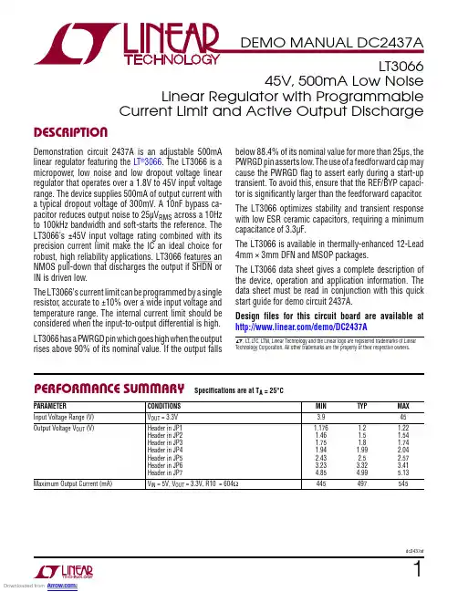
1dc2437afDescription45V, 500mA Low NoiseLinear Regulator with ProgrammableCurrent Limit and Active Output DischargeDemonstration circuit 2437A is an adjustable 500mA linear regulator featuring the L T ®3066. The LT3066 is a micropower , low noise and low dropout voltage linear regulator that operates over a 1.8V to 45V input voltage range. The device supplies 500mA of output current with a typical dropout voltage of 300mV. A 10nF bypass ca-pacitor reduces output noise to 25µV RMS across a 10Hz to 100kHz bandwidth and soft-starts the reference. The LT3066’s ±45V input voltage rating combined with its precision current limit make the IC an ideal choice for robust, high reliability applications. LT3066 features an NMOS pull-down that discharges the output if SHDN or IN is driven low.The LT3066’s current limit can be programmed by a single resistor , accurate to ±10% over a wide input voltage and temperature range. The internal current limit should be considered when the input-to-output differential is high. LT3066 has a PWRGD pin which goes high when the output rises above 90% of its nominal value. If the output fallsL , L T , L TC, L TM, Linear Technology and the Linear logo are registered trademarks of Linear Technology Corporation. All other trademarks are the property of their respective owners.performance summarybelow 88.4% of its nominal value for more than 25µs, the PWRGD pin asserts low. The use of a feedforward cap may cause the PWRGD flag to assert early during a start-up transient. To avoid this, ensure that the REF/BYP capaci-tor is significantly larger than the feedforward capacitor .The LT3066 optimizes stability and transient response with low ESR ceramic capacitors, requiring a minimum capacitance of 3.3µF.The LT3066 is available in thermally-enhanced 12-Lead 4mm × 3mm DFN and MSOP packages.The LT3066 data sheet gives a complete description of the device, operation and application information. The data sheet must be read in conjunction with this quick start guide for demo circuit 2437A.Design files for this circuit board are available athttp://www.linear .com/demo/DC2437ASpecifications are at T A = 25°CPARAMETERCONDITIONS MIN TYPMAX Input Voltage Range (V)V OUT = 3.3V 3.945Output Voltage V OUT (V)Header in JP1 Header in JP2 Header in JP3 Header in JP4 Header in JP5 Header in JP6 Header in JP71.176 1.46 1.75 1.942.433.234.85 1.2 1.5 1.8 1.99 2.5 3.32 4.99 1.22 1.54 1.74 2.04 2.57 3.415.13Maximum Output Current (mA)V IN = 5V, V OUT = 3.3V, R10 = 604Ω445497545Quick start proceDureDemonstration circuit 2437 is easy to set up to evaluate the performance of the LT3066. Refer to Figure 1 for proper measurement equipment setup and follow the procedure below:NOTE: Make sure that the input voltage does not exceed 45V.NOTE: The shutdown jumper JP2 shunt is required to be placed in the OFF or ON position for proper operation. NOTE: Place the output voltage selection jumper JP1 at the desired position.NOTE: Do not hot-plug the input voltage terminal V IN. The absolute maximum voltage on V IN is 50V and hot-plugging a power supply through wire leads to the demonstration circuit can cause the voltage on the extremely low ESR ceramic input capacitor to ring to twice its DC value. In order to protect the IC, a higher ESR Aluminum Electro-lytic capacitor is placed at the input terminals. This may protect against some, but not all, input transients due to hot-plugging with a power supply. See Application Note 88 for more details.NOTE: Connect the power supply (with power off), load, and meters as shown in Figure 1.1. After all connections are made, turn on the input power and verify the output voltage according to the output voltage selection jumper JP1. If the output voltage is different from the above values, use the USER option and install R8. Select R8 according to the following equation:R8 = (V OUT/0.6 – 1) • 61.9kNOTE: I f the output voltage is too low, temporarily disconnect the load to make sure that the load is not set too high.2. Once the proper output voltage is established, adjust the load within the operating range and observe the output voltage regulation, PWRGD and other parameters.2dc2437af3dc2437afQuick start proceDureFigure 1. Proper Measurement Equipment SetupFigure 2. Measuring Input or Output RippleOUTparts ListITEM QTY REFERENCE PART DESCRIPTION MANUFACTURER/PART NUMBER Required Circuit Components11C2CAP, 10µF, X7R, 50V, 10%, 1210MURATA, GRM32ER71H106KA12L23C3, C4, C5CAP, 3.3µF, X7R, 25V, 10%, 0805MURATA, GRM21BR71E335KA73L32C6, C7CAP, 0.01µF, X7R, 16V, 10%, 0603AVX, 0603YC103KAT2A41C8CAP, 0.022µF, X7R, 16V, 10%, 0603MURATA, GRM188R71C223KA01D51C9CAP, 0.47µF, X7R, 50V, 10%, 0603TDK, C1608X7R1H474K080AC62R1, R9RES, 61.9kΩ, 1%, 1/10W, 0603VISHAY, CRCW060361K9FKEA71R2RES, 93.1kΩ, 1%, 1/10W, 0603VISHAY, CRCW060393K1FKEA81R3RES, 124kΩ, 1%, 1/10W, 0603PANASONIC, ERJ3EKF1243V91R4RES, 143kΩ, 1%, 1/10W, 0603VISHAY, CRCW0603143KFKEA101R5RES, 196kΩ, 1%, 1/10W, 0603VISHAY, CRCW0603196KFKEA111R6RES, 280kΩ, 1%, 1/10W, 0603VISHAY, CRCW0603280KFKEA121R7RES, 453kΩ, 1%, 1/10W, 0603VISHAY, CRCW0603453KFKEA131R10RES, 604Ω, 1%, 1/10W, 0603VISHAY, CRCW0603604RFKEA141R11RES, 499kΩ, 1%, 1/10W, 0603PANASONIC, ERJ3EKF4993V151U1IC, LOW NOISE LINEAR REGULATOR, 4MM × 3MM, DFN LINEAR TECHNOLOGY, LT3066EDE#PBF Additional Demo Board Circuit Components10C1 (OPT)CAP, OPTION, ALUM ELECT, SMD20R8, R12, R13, R14RES, OPTION, 0603(OPT)Hardware: For Demo Board Only16E1, E2, E3, E4, E5,TEST POINT, TURRET, 0.094", MTG HOLE MILL-MAX, 2501-2-00-80-00-00-07-0 E621JP1CONN, HEADER, MALE, 2X8, 2MM, THT SAMTEC, TMM-108-02-L-D31JP2CONN, HEADER, MALE, 1X3, 2MM, THT SAMTEC, TMM-103-02-L-S42XJP1, XJP2CONN, SHUNT, FEMALE, 2 POS, 2MM SAMTEC, 2SN-BK-G4dc2437af5dc2437afI nformation furnished by Linear Technology Corporation is believed to be accurate and reliable. However , no responsibility is assumed for its use. Linear Technology Corporation makes no representa-tion that the interconnection of its circuits as described herein will not infringe on existing patent rights.schematic DiagramDEMONSTRATION BOARD IMPORTANT NOTICELinear Technology Corporation (LTC) provides the enclosed product(s) under the following AS IS conditions:This demonstration board (DEMO BOARD) kit being sold or provided by Linear Technology is intended for use for ENGINEERING DEVELOPMENT OR EVALUATION PURPOSES ONLY and is not provided by LTC for commercial use. As such, the DEMO BOARD herein may not be complete in terms of required design-, marketing-, and/or manufacturing-related protective considerations, including but not limited to product safety measures typically found in finished commercial goods. As a prototype, this product does not fall within the scope of the European Union directive on electromagnetic compatibility and therefore may or may not meet the technical requirements of the directive, or other regulations. If this evaluation kit does not meet the specifications recited in the DEMO BOARD manual the kit may be returned within 30 days from the date of delivery for a full refund. THE FOREGOING WARRANTY IS THE EXCLUSIVE WARRANTY MADE BY THE SELLER TO BUYER AND IS IN LIEU OF ALL OTHER WARRANTIES, EXPRESSED, IMPLIED, OR STATUTORY, INCLUDING ANY WARRANTY OF MERCHANTABILITY OR FITNESS FOR ANY PARTICULAR PURPOSE. EXCEPT TO THE EXTENT OF THIS INDEMNITY, NEITHER PARTY SHALL BE LIABLE TO THE OTHER FOR ANY INDIRECT, SPECIAL, INCIDENTAL, OR CONSEQUENTIAL DAMAGES.The user assumes all responsibility and liability for proper and safe handling of the goods. Further, the user releases LTC from all claims arising from the handling or use of the goods. Due to the open construction of the product, it is the user’s responsibility to take any and all appropriate precautions with regard to electrostatic discharge. Also be aware that the products herein may not be regulatory compliant or agency certified (FCC, UL, CE, etc.).No License is granted under any patent right or other intellectual property whatsoever. LTC assumes no liability for applications assistance, customer product design, software performance, or infringement of patents or any other intellectual property rights of any kind.LTC currently services a variety of customers for products around the world, and therefore this transaction is not exclusive.Please read the DEMO BOARD manual prior to handling the product. Persons handling this product must have electronics training and observe good laboratory practice standards. Common sense is encouraged.This notice contains important safety information about temperatures and voltages. For further safety concerns, please contact a LTC application engineer.Mailing Address:Linear Technology1630 McCarthy Blvd.Milpitas, CA 95035Copyright © 2004, Linear Technology Corporation6dc2437af Linear Technology Corporation LT 0116 • PRINTED IN USA。
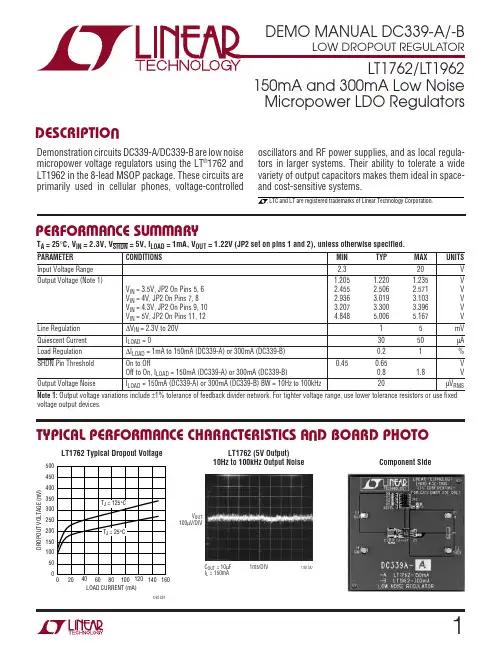
DC339-A -B低压差稳压器数据手册说明书
12REFERENCEDESIGNATOR QUANTITY PART NUMBER DESCRIPTION VENDOR TELEPHONE ADJ10Optional ResistorC110603ZG105ZAT1A1µF 10V Y5V Chip Capacitor AVX(843) 946-0362 C210402ZG104ZAT1A0.1µF 10V Y5V Chip Capacitor AVX(843) 946-0362 C31LMK325BJ106MN10µF 10V X7R Chip Capacitor Taiyo-Yuden(408) 573-4150 E1 to E442308-2Pad Turret Mill-Max(516) 922-6000 JP10Optional JumperJP216351-12G1Connector, SMT2X6, 0.39" Gap Comm-Con(626) 301-4200 Shunts for2CTAIJ1MM-G Shunts for 0.39" Gap Comm-Con(626) 301-4200 JP1 and JP2R11CR05-2613FM261k 1/16W 1% Chip Resistor AAC(800) 508-1521 R21CR05-3653FM365k 1/16W 1% Chip Resistor AAC(800) 508-1521 R31CR05-4223FM422k 1/16W 1% Chip Resistor AAC(800) 508-1521 R41CR05-7683FM768k 1/16W 1% Chip Resistor AAC(714) 255-9186 R51CR05-2493FM249k 1/16W 1% Chip Resistor AAC(714) 255-9186 U11LT1762EMS8 or8-Lead MSOP IC Version -A LTC(408) 432-1900 LT1962EMS88-Lead MSOP IC Version -BPARTS LISTOPERATIOUHOOK-UPSolid turret terminals are provided for easy connection to supplies and test equipment. Connect a 0V to 20V, 0.5A power supply across the IN and GND terminals and the load across the OUT and GND terminals. The SHDN pin can be disconnected from IN via JP1 to allow for separate shutdown control via a secondary control line. JP2 can be used to select any of a number of common fixed output voltages, or used in conjunction with ADJ1 to create a custom output voltage using the formula:ADJ1 = (V OUT – 1.22V)/4.93µAOUTPUT CAPACITOR SELECTIONThe output capacitor C3 is a 10µF X7R ceramic chip capacitor. Should a different output capacitor be desired, care must be exercised with the selection. Many ceramic capacitor dielectrics exhibit strong temperature and voltage characteristics that reduce their effective capaci-tance to as low as 10% to 20% of nominal over the full range. For further information, see Linear Technology Application Note 83, “Performance Verification of Low Noise, Low Dropout Regulators,” Appendix␣B, “Capaci-tor Selection Considerations,” reprinted below.CAPACITOR SELECTION CONSIDERATIONSBypass Capacitance and Low Noise Performance Adding a capacitor between the regulator’s V OUT and BYP pins lowers output noise. A good quality, low leakage capacitor is recommended. This capacitor bypasses the regulator’s reference, providing a low frequency noise pole. A 0.01µF capacitor lowers the output voltage noise to 20µV RMS. Using a bypass capacitor also improves transient response. With no bypassing and a 10µF output capacitor, a 10mA to 500mA load step settles within 1% of final value in under 100µs. With a 0.01µF bypass capacitor, the output settles within 1% for the same load step in under 10µs; total output deviation is inside 2.5%. Regulator start-up time is inversely proportional to bypass capacitor size, slowing to 15ms with a 0.01µF bypass capacitor and 10µF at the output.34567Information furnished by Linear Technology Corporation is believed to be accurate and reliable.However, no responsibility is assumed for its use. Linear Technology Corporation makes no represen-tation that the interconnection of its circuits as described herein will not infringe on existing patent rights.8dc339 LT/TP 0301 500 • PRINTED IN USA© LINEAR TECHNOLOGY CORPORA TION 2001Linear Technology Corporation1630 McCarthy Blvd., Milpitas, CA 95035-7417(408) 432-1900 q FAX: (408) 434-0507 q 。
MAX8510 MAX8511 MAX8512 极低噪声、低掉电的线性调压器说明说明书

General DescriptionThe MAX8510/MAX8511/MAX8512 ultra-low-noise, low-dropout (LDO) linear regulators are designed to deliver up to 120mA continuous output current. These regulators achieve a low 120mV dropout for 120mA load current. The MAX8510 uses an advanced architecture to achieve ultra-low output voltage noise of 11μV RMS and PSRR of 54dB at 100kHz.The MAX8511 does not require a bypass capacitor, hence achieving the smallest PC board area. The MAX8512’s output voltage can be adjusted with an external divider.The MAX8510/MAX8511 are preset to a variety of voltag-es in the 1.5V to 4.5V range. Designed with a P-channel MOSFET series pass transistor, the MAX8510/MAX8511/MAX8512 maintain very low ground current (40μA).The regulators are designed and optimized to work with low-value, low-cost ceramic capacitors. The MAX8510 requires only 1μF (typ) of output capacitance for stability with any load. When disabled, current consumption drops to below 1μA.Package options include a 5-pin SC70 and a tiny 2mm x 2mm x 0.8mm TDFN package.Applications●Cellular and Cordless Phones ●PDA and Palmtop Computers ●Base Stations●Bluetooth Portable Radios and Accessories ●Wireless LANs ●Digital Cameras ●Personal Stereos●Portable and Battery-Powered EquipmentFeatures●Space-Saving SC70 and TDFN (2mm x 2mm) Packages ●11μV RMS Output Noise at 100Hz to 100kHzBandwidth (MAX8510)●78dB PSRR at 1kHz (MAX8510) ●120mV Dropout at 120mA Load●Stable with 1μF Ceramic Capacitor for Any Load ●Guaranteed 120mA Output●Only Need Input and Output Capacitors (MAX8511) ●Output Voltages: 1.5V, 1.8V, 2.5V, 2.6V, 2.7V, 2.8V,2.85V, 3V,3.3V,4.5V (MAX8510/MAX8511) and Adjustable (MAX8512) ●Low 40μA Ground Current ●Excellent Load/Line Transient●Overcurrent and Thermal Protection19-2732; Rev 5; 5/19Output Voltage Selector Guide appears at end of data sheet.Ordering Information continued at end of data sheet.*xy is the output voltage code (see Output Voltage Selector Guide). Other versions between 1.5V and 4.5V are available in 100mV increments. Contact factory for other versions.+Denotes a lead(Pb)-free/RoHS-compliant package.T = Tape and reel.PART*TEMP RANGE PIN-PACKAGEMAX8510EXKxy+T -40°C to +85°C 5 SC70MAX8510/MAX8511/MAX8512Ultra-Low-Noise, High PSRR,Low-Dropout, 120mA Linear RegulatorsOrdering InformationClick here for production status of specific part numbers.IN to GND ................................................................-0.3V to +7V Output Short-Circuit Duration ...........................................Infinite OUT, SHDN to GND .....................................-0.3V to (IN + 0.3V)FB, BP , N.C. to GND ................................-0.3V to (OUT + 0.3V)Continuous Power Dissipation (T A = +70°C)5-Pin SC70 (derate 3.1mW/°C above +70°C) .............0.247W 8-Pin TDFN (derate 11.9mW/°C above = 70°C) .........0.953W Operating Temperature Range ...........................-40°C to +85°CMilitary Operating Temperature Range .............-55°C to +110°C Junction Temperature ......................................................+150°C Storage Temperature Range ............................-65°C to +150°C Lead Temperature (soldering, 10s) .................................+300°C Soldering Temperature (reflow) .......................................+260°C Lead (Pb)-free packages .................................................+260°C Packages containing lead (Pb) .......................................+240°C(Note 1)SC70Junction-to-Ambient Thermal Resistance (θJA ) ........324°C/W Junction-to-Case Thermal Resistance (θJC ) .............115°C/WTDFNJunction-to-Ambient Thermal Resistance (θJA ) .......83.9°C/W Junction-to-Case Thermal Resistance (θJC ) ...............37°C/W(V IN = V OUT + 0.5V, T A = -40°C to +85°C, unless otherwise noted. C IN = 1μF, C OUT = 1μF, C BP = 10nF. Typical values are at +25°C; the MAX8512 is tested with 2.45V output, unless otherwise noted.) (Note 2)PARAMETER SYMBOL CONDITIONSMIN TYPMAX UNITS Input Voltage Range V IN26VOutput Voltage Accuracy I OUT = 1mA, T A = +25°C-1+1%I OUT = 100µA to 80mA, T A = +25°C -2+2I OUT = 100µA to 80mA-3+3Maximum Output Current I OUT 120mA Current LimitI LIMV OUT = 90% of nominal value 130200300mA Dropout Voltage (Note 3)V OUT ≥ 3V, I OUT = 80mA 80170mVV OUT ≥ 3V, I OUT = 120mA1202.5V ≤ V OUT < 3V, I OUT = 80mA 902002.5V ≤ V OUT < 3V, I OUT = 120mA 1352V ≤ V OUT < 2.5V, I OUT = 80mA 1202502V ≤ V OUT < 2.5V, I OUT = 120mA180Ground Current I Q I OUT = 0.05mA4090µA V IN = V OUT (nom) - 0.1V, I OUT = 0mA 220500Line Regulation V LNR V IN = (V OUT + 0.5V) to 6V, I OUT = 0.1mA 0.001%/V Load RegulationV LDR I OUT = 1mA to 80mA 0.003%/mA Shutdown Supply CurrentI SHDNV SHDN = 0VT A = +25°C 0.0031µAT A = +85°C 0.05Ripple RejectionPSRRf = 1kHz, I OUT = 10mAMAX851078dBMAX8511/MAX851272f = 10kHz, I OUT = 10mA MAX851075MAX8511/MAX851265f = 100kHz, I OUT = 10mAMAX851054MAX8511/ MAX851246MAX8512Low-Dropout, 120mA Linear RegulatorsAbsolute Maximum RatingsStresses beyond those listed under “Absolute Maximum Ratings” may cause permanent damage to the device. These are stress ratings only, and functional operation of the device at these or any other conditions beyond those indicated in the operational sections of the specifications is not implied. Exposure to absolute maximum rating conditions for extended periods may affect device reliability.Electrical CharacteristicsPackage Thermal Characteristics Note 1: Package thermal resistances were obtained using the method described in JEDEC specification JESD51-7, using a four-layerboard. For detailed information on package thermal considerations, refer to /thermal-tutorial .(V IN = V OUT + 0.5V, T A = -40°C to +85°C, unless otherwise noted. C IN = 1μF, C OUT = 1μF, C BP = 10nF. Typical values are at +25°C; the MAX8512 is tested with 2.45V output, unless otherwise noted.) (Note 2)Note 2: Limits are 100% tested at +25°C. Limits over operating temperature range are guaranteed by design.Note 3: Dropout is defined as V IN - V OUT when V OUT is 100mV below the value of V OUT for V IN = V OUT + 0.5V.Note 4: Time needed for V OUT to reach 90% of final value.(V IN = V OUT + 0.5V, C IN = 1μF, C OUT = 1μF, C BP = 10nF, T A = +25°C, unless otherwise noted.)PARAMETER SYMBOLCONDITIONSMINTYP MAXUNITSOutput Noise Voltage (RMS)f = 100Hz to 100kHz, I LOAD = 10mA MAX851011µVMAX8511/MAX8512230f = 100Hz to 100kHz, I LOAD = 80mA MAX851013MAX8511/MAX8512230Shutdown Exit Delay R LOAD = 50Ω (Note 4)300µs SHDN Logic Low Level V IN = 2V to 6V 0.4V SHDN Logic High Level V IN = 2V to 6V 1.5V SHDN Input Bias Current V IN = 6V, V SHDN = 0V or 6VT A = +25°C µA T A = +85°C 0.01FB Input Bias Current (MAX8512)V IN = 6V,V FB = 1.3VT A = +25°C 0.0060.1µA T A = +85°C0.01Thermal Shutdown 160°C Thermal-Shutdown Hysteresis10°C MAX8510OUTPUT VOLTAGE ACCURACYvs. LOAD CURRENTM A X 8510 t o c 02LOAD CURRENT (mA)% D E V I A T I O N (%)10080604020-0.4-0.200.20.40.6-0.60120MAX8510OUTPUT VOLTAGE ACCURACYvs. TEMPERATURETEMPERATURE (°C)% D E V I A T I O N (%)603510-15-0.8-0.6-0.4-0.200.20.40.60.81.0-1.0-4085MAX8510OUTPUT VOLTAGE vs. INPUT VOLTAGEINPUT VOLTAGE (V)O U T P U T V O L T A G E (V )543210.51.01.52.02.53.00.06MAX8512Low-Dropout, 120mA Linear RegulatorsElectrical Characteristics (continued)Typical Operating Characteristics(V IN = V OUT + 0.5V, C IN = 1μF, C OUT = 1μF, C BP = 10nF, T A = +25°C, unless otherwise noted.)MAX8510DROPOUT VOLTAGE vs. OUTPUT VOLTAGEOUTPUT (V)D R O P O U T V O L T A G E (m V )3.02.82.62.42.2501001502002502.03.2MAX8510GROUND PIN CURRENT vs. TEMPERATUREM A X 8510 t o c 08TEMPERATURE (°C)G R O U N D P I N C U R R E N T (µA )603510-153540455030-4085MAX8510OUTPUT NOISE400µs/divMAX8510GROUND PIN CURRENT vs. INPUT VOLTAGEINPUT VOLTAGE (V)G R O U N D P I N C U R R E N T (µA )43211502005010025030035005MAX8510PSRR vs. FREQUENCYFREQUENCY (kHz)P S R R (d B )1101000.14050601020307080900.011000MAX8510OUTPUT NOISE SPECTRAL DENSITYvs. FREQUENCYMAX8510 toc12FREQUENCY (kHz)O U T P U T N O I S E D E N S I T Y (n V /H z )0.11101001.E+031.E+021.E+041.E+010.011000MAX8510DROPOUT VOLTAGE vs. LOAD CURRENTLOAD CURRENT (mA)D R O P O U T V O L T A G E (m V )1008060402030609012015000120MAX8510GROUND PIN CURRENT vs. LOAD CURRENTLOAD CURRENT (mA)G R O U N D P I N C U R R E N T (µA )10080604020408012016020024000120MAX8511PSRR vs. FREQUENCYFREQUENCY (kHz)P S R R (d B )0.111010040506010203070809000.011000MAX8512Low-Dropout, 120mA Linear RegulatorsTypical Operating Characteristics (continued)(V IN = V OUT + 0.5V, C IN = 1μF, C OUT = 1μF, C BP = 10nF, T A= +25°C, unless otherwise noted.)MAX8510LOAD TRANSIENT RESPONSE1ms/div V OUT 10mV/divMAX8510EXITING SHUTDOWN WAVEFORM20µs/divV OUT = 2.85VR LOAD = 47ΩOUTPUT VOLTAGE 2V/divSHUTDOWN VOLTAGEMAX8510LOAD TRANSIENT RESPONSE NEAR DROPOUT1ms/divV OUT 10mV/divMAX8510ENTERING SHUTDOWN DELAY40µs/divC BP = 0.01µFOUTPUT VOLTAGE 2V/divSHUTDOWN VOLTAGEMAX8510REGION OF STABLE C OUT ESRvs. LOAD CURRENTM A X 8510 t o c 20LOAD CURRENT (mA)C O U T E S R (Ω)806040200.11101000.01120100STABLE REGIONMAX8510OUTPUT NOISE vs. BP CAPACITANCEM A X 8510 t o c 13BP CAPACITANCE (nF)O U T P U T N O I S E (µV )1051015202501100MAX8510LINE TRANSIENT RESPONSE200µs/divV IN = 3.5V TO 4VV OUT 2mV/divMAX8510SHUTDOWN EXIT DELAY20µs/divV OUT 1V/divSHUTDOWN VOLTAGEV OUT = 3V C BP = 100nFMAX8512Low-Dropout, 120mA Linear RegulatorsTypical Operating Characteristics (continued)Detailed DescriptionThe MAX8510/MAX8511/MAX8512 are ultra-low-noise, low-dropout, low-quiescent current linear regulators designed for space-restricted applications. The parts are available with preset output voltages ranging from 1.5V to 4.5V in 100mV increments. These devices can supply loads up to 120mA. As shown in the Functional Diagram , the MAX8510/MAX8511 consist of an innovative bandgap core and noise bypass circuit, error amplifier, P-channel pass transistor, and internal feedback voltage-divider. The MAX8512 allows for adjustable output with an external feedback network.The 1.225V bandgap reference is connected to the error amplifier’s inverting input. The error amplifier compares this reference with the feedback voltage and amplifies the difference. If the feedback voltage is lower than the refer-ence voltage, the pass-transistor gate is pulled low. This allows more current to pass to the output and increases the output voltage. If the feedback voltage is too high, the pass transistor gate is pulled high, allowing less cur-rent to pass to the output. The output voltage is fed back through an internal resistor voltage-divider connected to the OUT pin.An external bypass capacitor connected to BP (MAX8510) reduces noise at the output. Additional blocks include a current limiter, thermal sensor, and shutdown logic.Internal P-Channel Pass TransistorThe MAX8510/MAX8511/MAX8512 feature a 1Ω (typ) P-channel MOSFET pass transistor. This provides sev-eral advantages over similar designs using a PNP pass transistor, including longer battery life. The P-channel MOSFET requires no base drive, which considerably reduces quiescent current. PNP-based regulators waste considerable current in dropout when the pass transistor saturates. They also use high base-drive current under heavy loads. The MAX8510/MAX8511/MAX8512 do not suffer from these problems and consume only 40μA of quiescent current in light load and 220μA in dropout (see the Typical Operating Characteristics ).Output Voltage SelectionThe MAX8510/MAX8511 are supplied with factory-set output voltages from 1.5V to 4.5V, in 100mV increments (see Ordering Information ). The MAX8512 features a user-adjustable output through an external feedback net-work (see the Typical Operating Circuits ).To set the output of the MAX8512, use the following equa-tion:OUT REF V R1R2X -1V=where R2 is chosen to be less than 240kΩ and V REF = 1.225V. Use 1% or better resistors.PINNAMEFUNCTIONMAX8510MAX8511MAX8512SC70TDFN -EP SC70TDFN -EP SC70TDFN -EP 151515IN Unregulated Input Supply 232323GNDGround343434SHDN Shutdown. Pull low to disable the regulator.42————BP Noise Bypass for Low-Noise Operation. Connect a 10nF capacitor from BP to OUT. BP is shorted to OUT in shutdown mode.————42FB Adjustable Output Feedback Point575757OUT Regulated Output Voltage. Bypass with a capacitor to GND. See the Capacitor Selection and Regulator Stability section for more details.—1, 6, 841, 2, 6,—1, 6, 8N.C.No connection. Not internally connected.——————EPExposed Pad (TDFN Only). Internally connected to GND. Connect to a large ground plane to maximize thermal performance. Not intended as an electrical connection point.MAX8512Low-Dropout, 120mA Linear RegulatorsPin DescriptionShutdownThe MAX8510/MAX8511/MAX8512 feature a low-power shutdown mode that reduces quiescent current less than 1μA. Driving SHDN low disables the voltage reference, error amplifier, gate-drive circuitry, and pass transistor (see the Functional Diagram), and the device output enters a high-impedance state. Connect SHDN to IN for normal operation.Current LimitThe MAX8510/MAX8511/MAX8512 include a current lim-iter, which monitors and controls the pass transistor’s gate voltage, limiting the output current to 200mA. For design purposes, consider the current limit to be 130mA (min) to 300mA (max). The output can be shorted to ground for an indefinite amount of time without damaging the part. Thermal-Overload ProtectionThermal-overload protection limits total power dissipation in the MAX8510/MAX8511/MAX8512. When the junction temperature exceeds T J = +160°C, the thermal sensor signals the shutdown logic, turning off the pass transis-tor and allowing the IC to cool down. The thermal sensor turns the pass transistor on again after the IC’s junction temperature drops by 10°C, resulting in a pulsed output during continuous thermal-overload conditions.Thermal-overload protection is designed to protect the MAX8510/MAX8511/MAX8512 in the event of a fault con-dition. For continual operation, do not exceed the abso-lute maximum junction temperature rating of T J = +150°C. Operating Region and Power DissipationThe MAX8510/MAX8511/MAX8512 maximum power dis-sipation depends on the thermal resistance of the case and circuit board, the temperature difference between the die junction and ambient, and the rate of airflow. The power dissipation across the device is:P = I OUT (V IN - V OUT)The maximum power dissipation is:P MAX = (T J - T A) / (θJC + θCA)where T J - T A is the temperature difference between the MAX8510/MAX8511/MAX8512 die junction and the sur-rounding air, θJC is the thermal resistance of the package, and θCA is the thermal resistance through the PC board, copper traces, and other materials to the surrounding air. The GND pin of the MAX8510/MAX8511/MAX8512 per-forms the dual function of providing an electrical connec-tion to ground and channeling heat away. Connect the GND pin to ground using a large pad or ground plane.Noise ReductionFor the MAX8510, an external 0.01μF bypass capaci-tor between BP and OUT with innovative noise bypass scheme reduces output noises dramatically, exhibiting 11μV RMS of output voltage noise with C BP = 0.01μF and C OUT = 1μF. Startup time is minimized by a poweron cir-cuit that precharges the bypass capacitor. Applications InformationCapacitor Selectionand Regulator StabilityUse a 1μF capacitor on the MAX8510/MAX8511/MAX8512 input and a 1μF capacitor on the output. Larger input capacitor values and lower ESRs provide better noise rejection and line-transient response. Reduce output noise and improve load-transient response, stability, and power-supply rejection by using large output capacitors. Note that some ceramic dielectrics exhibit large capaci-tance and ESR variation with temperature. With dielec-trics such as Z5U and Y5V, it may be necessary to use a 2.2μF or larger output capacitor to ensure stability at temperatures below -10°C. With X7R or X5R dielectrics, 1μF is sufficient at all operating temperatures. A graph of the region of stable C OUT ESR vs. load current is shown in the Typical Operating Characteristics.Use a 0.01μF bypass capacitor at BP (MAX8510) for low-output voltage noise. The leakage current going into the BP pin should be less than 10nA. Increasing the capaci-tance slightly decreases the output noise. Values above 0.1μF and below 0.001μF are not recommended. Noise, PSRR, and Transient ResponseThe MAX8510/MAX8511/MAX8512 are designed to deliv-er ultra-low noise and high PSRR, as well as low dropout and low quiescent currents in battery-powered systems. The MAX8510 power-supply rejection is 78dB at 1kHz and 54dB at 100kHz. The MAX8511/MAX8512 PSRR is 72dB at 1kHz and 46dB at 100kHz (see the Power-Supply Rejection Ratio vs. Frequency graph in the Typical Operating Characteristics).When operating from sources other than batteries, improved supply-noise rejection and transient response can be achieved by increasing the values of the input and output bypass capacitors, and through passive filter-ing techniques. The Typical Operating Characteristics show the MAX8510/MAX8511/MAX8512 line- and load-transient responses.MAX8512Low-Dropout, 120mA Linear RegulatorsDropout VoltageA regulator’s minimum dropout voltage determines the lowest usable supply voltage. In battery-powered sys-tems, this determines the useful end-of-life battery volt-age. Because the MAX8510/MAX8511/MAX8512 use aP-channel MOSFET pass transistor, their dropout voltage is a function of drain-to-source on-resistance (RDS(ON)) multiplied by the load current (see the Typical Operating Characteristics ).MAX8512Low-Dropout, 120mA Linear RegulatorsFunctional Diagram*xy is the output voltage code (see Output Voltage Selector Guide). Other versions between 1.5V and 4.5V are available in 100mV increments. Contact factory for other versions.**EP = Exposed pad.+Denotes a lead(Pb)-free/RoHS-compliant package.T = Tape and reel.(Note: Standard output voltage options, shown in bold , are available. Contact the factory for other output voltages between 1.5V and 4.5V. Minimum order quantity is 15,000 units.)PART*TEMP RANGE PIN-PACKAGE MAX8510MXK33/PR3+-55°C to +110°C 5 SC70MAX8510ETAxy+T -40°C to +85°C 8 TDFN-EP** 2mm x 2mm MAX8511EXKxy+T -40°C to +85°C 5 SC70MAX8511ETAxy+T -40°C to +85°C 8 TDFN-EP** 2mm x 2mm MAX8512EXK+T -40°C to +85°C 5 SC70MAX8512ETA+T-40°C to +85°C8 TDFN-EP** 2mm x 2mmPARTV OUT (V)TOP MARKMAX8510EXK16+T 1.6AEX MAX8510EXK18+T 1.8AEA MAX8510ETA25+T 2.5AAO MAX8510EXK27+T 2.7ATD MAX8510ETA28+T 2.8AAR MAX8510EXK29+T 2.85ADS MAX8510MXK33/PR3+ 3.3AUV MAX8510ETA30+T 3AAS MAX8510ETA33+T 3.3AAT MAX8510ETA45+T 4.5AAU MAX8510MXK33/PR3+ 3.3AUV MAX8511EXK15+T 1.5ADU MAX8511ETA18+T 1.8AAV MAX8511ETA25+T 2.5AAP MAX8511ETA26+T 2.6AAW MAX8511EXK28+T 2.8AFA MAX8511ETA29+T 2.85AAX MAX8511EXK89+T 2.9AEH MAX8511EXK31+T 3.1ARS MAX8511ETA33+T 3.3AAY MAX8511EXK45+T4.5AEJ MAX8512ETA+TAdjustableAAQPACKAGE TYPE PACKAGE CODE OUTLINE ND PATTERN NO.8 TDFN T822+121-016890-00645 SC70X5+121-007690-0188MAX8512Low-Dropout, 120mA Linear RegulatorsTypical Operating Circuits (continued)Ordering Information (continued)Output Voltage Selector GuidePackage InformationFor the latest package outline information and land patterns (footprints), go to /packages . Note that a “+”, “#”, or “-” in the package code indicates RoHS status only. Package drawings may show a different suffix character, but the drawing pertains to the package regardless of RoHS status.Chip InformationPROCESS: BiCMOSREVISION NUMBERREVISION DATE DESCRIPTIONPAGES CHANGED 48/11Corrected errors and added lead-free packages 1, 2, 3, 6, 955/19Updated Output Voltage Selector Guide9Maxim Integrated cannot assume responsibility for use of any circuitry other than circuitry entirely embodied in a Maxim Integrated product. No circuit patent licenses are implied. Maxim Integrated reserves the right to change the circuitry and specifications without notice at any time. The parametric values (min and max limits) shown in the Electrical Characteristics table are guaranteed. Other parametric values quoted in this data sheet are provided for guidance.MAX8512Low-Dropout, 120mA Linear RegulatorsRevision HistoryFor pricing, delivery, and ordering information, please visit Maxim Integrated’s online storefront at https:///en/storefront/storefront.html.。
500mA 低噪声 LDO 电压调节器 使用手册说明书
Rev. 2.0.5GENERAL DESCRIPTIONThe SPX3819 is a positive voltage regulator with a low dropout voltage and low noise output. In addition, this device offers a very low ground current of 800μA at 100mA output. The SPX3819 has an initial tolerance of less than 1% max and a logic compatible ON/OFF switched input. When disabled, power consumption drops to nearly zero. Other key features include reverse battery protection, current limit, and thermal shutdown. The SPX3819 includes a reference bypass pin for optimal low noise output performance. With its very low output temperature coefficient, this device also makes a superior low power voltage reference.The SPX3819 is an excellent choice for use in battery-powered applications such as cordless telephones, radio control systems, and portable computers. It is available in several fixed output voltage options or with an adjustable output voltage.This device is offered in 8 pin NSOIC, 8 pin DFN and 5-pin SOT-23 packages. APPLICATIONS•Portable Consumer Equipment •Portable Instrumentation•Industrial Equipment•SMPS Post RegulatorsFEATURES•Low Noise: 40μV Possible•High Accuracy: 1%•Reverse Battery Protection•Low Dropout: 340mV at Full Load•Low Quiescent Curre nt: 90μA•Zero Off-Mode Current•Fixed & Adjustable Output Voltages: −1.2V, 1.5V, 1.8V, 2.5V, 3.0V, 3.3V & 5.0VFixed Output Voltages−≥1.235V Adjustable Output Voltages •Available in RoHS Compliant, Lead Free Packages:−5-pin SOT-23, 8-pin SOIC and 8-pin DFNTYPICAL APPLICATION DIAGRAMFig. 1: SPX3819 Application CircuitABSOLUTE MAXIMUM RATINGSThese are stress ratings only and functional operation of the device at these ratings or any other above those indicated in the operation sections of the specifications below is not implied. Exposure to absolute maximum rating conditions for extended periods of time may affect reliability.V IN, EN ..................................................... -20V to +20V Storage Temperature .............................. -65°C to 150°C Junction Temperature .......................................... 150°C Power Dissipation ................................ Internally Limited Lead Temperature (Soldering, 5 sec) ..................... 260°C ESD Rating (HBM - Human Body Model) .................... 1kV OPERATING RATINGSInput Voltage Range V IN................................ 2.5V to 16V Enable Pin EN ............................................... 0.0V to V IN Junction Temperature Range ................. -40°C to +125°C Thermal Resistance1..................................................... θJA (SOT23-5) ...............................................191°C/W θJA (NSOIC-8) ............................................ 128.4°C/W θJA (DFN-8) ................................................... 59°C/W Note 1: The maximum allowable power dissipation is a function of maximum operating junction temperature, T J(max) the junction to ambient thermal resistance, and theambient θJA, and the ambient temperature T A. The maximum allowable power dissipation at any ambient temperature is given: P D(max)= (T J(max)-T A)/θJA, exceeding the maximum allowable power limit will result in excessive die temperature; thus, the regulator will go into thermal shutdown.ELECTRICAL SPECIFICATIONSSpecifications with standard type are for an Operating Junction Temperature of T J = 25°C only; limits applying over the full Operating Junction Temperature range are denoted by a “•”. Minimum and Maximum limits are guaranteed through test, design, or statistical correlation. Typical values represent the most likely parametric norm at T J = 25°C, and are provided for reference purposes only. Unless otherwise indicated, V IN = V OUT + 1V (V IN = V OUT + 1.2V for 1.2V option), I L= 100µA, C L = 1µF, V EN≥ 2.5V, T A= T J = 25°C.Parameter Min. Typ. Max. Units ConditionsOutput Voltage Tolerance -1 +1%-2 +2 •Output Voltage TemperatureCoefficient 57 ppm/°CLine Regulation 0.04 0.1%/VV IN = V OUT +1 to 16V and V EN≤ 6V0.2 • V IN = V EN = V OUT +1 ≤ 8V0.2 V IN = V EN = V OUT +1 ≤16VT A = 25°C to 85°CLoad Regulation 0.05 0.4 % I L= 0.1mA to 500mADropout Voltage (V IN-V OUT) 210 60mVI L = 100µA80 •125 175I L= 50mA250 •180 350I L= 150mA450 •340 550I L= 500mA700 •Quiescent Current (I GND) 0.05 3µAV ENABLE≤ 0.4V8 • V ENABLE = 0.25VGround Pin Current (I GND) 90 150µAI L = 100µA190 •250 650I L= 50mA900 •1.02.0mAI L= 150mA2.5 •6.5 25.0I L= 500mA30.0 •Ripple Rejection (PSRR) 70 dBParameterMin. Typ. Max. Units ConditionsCurrent Limit (I LIMIT )800 mAV OUT =0V 950 • Output Noise (e NO )300 µV RMS I L = 10mA, C L = 1.0µF, C IN = 1µF, (10Hz – 100kHz)40 µV RMS I L = 10mA, C L = 1.0µF, C BYP = 1µF, C IN = 1µF, (10Hz – 100kHz) Input Voltage Level Logic Low (V IL )0.4 V OFF Input Voltage Level Logic High (V IH )2 V ONENABLE Input Current0.01 2 µAVIL ≤ 0.4V VIH ≥ 2.0V320Note 2: Not applicable to output voltage 2V or less.PIN ASSIGNMENTFig. 2: SPX3819 Pin AssignmentPIN DESCRIPTIONName Pin #nSOICPin # DFN Pin # SOT-23 DescriptionVIN 2 3 1 Supply Input GND 5, 6, 7, 87 2 GroundVOUT 3 5 5 Regulator OutputEN 113Enable(input). CMOS compatible control input. Logic high – enable; logic low or open = shutdownADJ 4 8 4Adjust able part only. Feedback input. Connect to resistive voltage-divider networkBYP Fixed version only. Internal reference bypass pin. Connect 10nF to ground to reduce thermal noise on the output. NC-2, 4, 6-No ConnectORDERING INFORMATION(1)Part Number Operating Temperature Range Lead-Free Package Packaging Method SPX3819M5-L/TR-40°C≤T J≤+125°C Yes(2)SOT-23-5Tape & ReelSPX3819M5-L-1-2/TRSPX3819M5-L-1-5/TRSPX3819M5-L-1-8/TRSPX3819M5-L-2-5/TRSPX3819M5-L-3-0/TRSPX3819M5-L-3-3/TRSPX3819M5-L-5-0/TRSPX3819R2-L/TRDFN-8 SPX3819R2-L-1-2/TRSPX3819S-L/TRNSOIC-8 SPX3819S-L-5-0/TRNOTES:1.Refer to /SPX3819 for most up-to-date Ordering Information2.Visit for additional information on Environmental Rating.TYPICAL PERFORMANCE CHARACTERISTICSFig. 3: Ground Current vs Load Current Fig. 4: Ground Current vs Input VoltageFig. 5 Ground Current vs Load Current in Dropout Fig. 6 Output Voltage vs Input VoltageFig. 7 Dropout Voltage vs Load Current Fig. 8 Output Voltage vs Load CurrentFig. 9 Ground Current vs Temperature with 100μA LoadFig. 10 Ground Current vs Temperature with 50mA LoadFig. 11 Ground Current vs Temperature with 500mA LoadFig. 12 Ground Current vs Temperature in DropoutFig. 13 ENABLE Voltage, ON threshold, vs Input VoltageFig. 14 Output Voltage vs TemperatureFig. 15 Output Noise vs Bypass Capacitor Value IL = 10mA,10Hz - 100kHzFig. 16 Line Transient Response for 3.3V DeviceFig. 17 Load Transient Response for 3.3V DeviceAPPLICATION INFORMATIONThe SPX3819 requires an output capacitor for device stability. Its value depends upon the application circuit. In general, linear regulator stability decreases with higher output currents.In applications where the SPX3819 is sourcing less current, a lower output capacitance may be sufficient. For example, a regulator outputting only 10mA, requires approximately half the capacitance as the same regulator sourcing 150mA.Bench testing is the best method for determining the proper type and value of the capacitor since the high frequency characteristics of electrolytic capacitors vary widely, depending on type and manufacturer. A high quality 2.2μF aluminum electrolytic capacitor works in most application circuits, but the same stability often can be obtained with a1μF tantalum electrolytic.With the SPX3819 adjustable version, the minimum value of output capacitance is a function of the output voltage. The value decreases with higher output voltages, since closed loop gain is increased.T YPICAL A PPLICATIONS C IRCUITSFor fixed voltage options only. A 10nF capacitor on the BYP pin will significantly reduce output noise, but it may be left unconnected if the output noise is not a major concern. The SPX3819 start-up speed is inverselyproportional to the size of the BYP capacitor.Applications requiring a slow rampup of the output voltage should use a larger CBYP. However, if a rapid turn-on is necessary, the BYP capacitor can be omitted.The SPX3819’s internal reference is available through the BYP pin.Figure 18 represents a SPX3819 standard application circuit. The EN (enable) pin is pulled high (>2.0V) to enable the regulator. To disable the regulator, EN < 0.4V.Fig. 18: Standard Application Circuit The SPX3819 in Figure 19 illustrates a typical adjustable output voltage configuration. Two resistors (R1 and R2) set the output voltage. The output voltage is calculated using the formula:VOUT = 1.235V x [1 + R1/R2]R2 must be >10kΩand for best results, R2 should be bet ween 22kΩ and 47kΩ.Fig. 19: Typical Adjustable Output Voltage ConfigurationMECHANICAL DIMENSIONS 8-PIN SOICNMECHANICAL DIMENSIONS(CONTINUED) 8-PIN 2X3DFNRECOMMENDED LAND PATTERN AND STENCIL8-PIN 2X3DFNMECHANICAL DIMENSIONS(CONTINUED) 5-PIN SOT-23REVISION HISTORY RevisionDate Description 2.0.008/23/12 Reformat of Datasheet Addition of SPX3819R2-L and SPX3819R2-L/TR part numbers 2.0.112/02/13 Added Storage Temperature Range and Junction Temperature in ABS MAX Ratings.2.0.205/20/14 Updated package drawings and corrected DFN-8 package marking information [ECN 1423-03 6/3/14] 2.0.308/31/16 Updated logo and Ordering Information table. 2.0.407/19/18 Update to MaxLinear logo. Updated format and Ordering Information. Clarified ADJ and BYP pin. Correct y-axis on Figure 14. Updated ESD rating. 2.0.5 12/05/19 Corrected table alignment on last 5 specs of the Electrical Specifications table.C ORPORATE H EADQUARTERS :5966 La Place CourtSuite 100Carlsbad, CA 92008Tel.: +1 (760) 692-0711Fax: +1 (760) 444-8598The content of this document is furnished for informational use only, is subject to change without notice, and should not be construed as a commitment by Maxlinear, Inc. Maxlinear, I nc. Assumes no responsibility or liability for any errors or inaccuracies that may appear in the informational content contained in this guide. Complying with all applicable copyright laws is the responsibility of the user. Without limiting the rights under copyright, no part of this document may be reproduced into, stored in, or introduced into a retrieval system, or transmitted in any form or by any means (electronic, mechanical, photocopying, recording, or otherwise), or for any purpose, without the express written permission of Maxlinear, Inc.Maxlinear, Inc. Does not recommend the use of any of its products in life support applications where the failure or malfunction of the product can reasonably be expected to cause failure of the life support system or to significantly affect its safety or effectiveness. Products are not authorized for use in such applications unless Maxlinear, Inc. Receives, in writing, assurances to its satisfaction that: (a) the risk of injury or damage has been minimized; (b) the user assumes all such risks; (c) potential liability of Maxlinear, Inc. Is adequately protected under the circumstances.Maxlinear, Inc. May have patents, patent applications, trademarks, copyrights, or other intellectual property rights covering subject matter in this document. Except as expressly provided in any written license agreement from Maxlinear, Inc., the furnishing of this document does not give you any license to these patents, trademarks, copyrights, or other intellectual property.Maxlinear, the Maxlinear logo, and any Maxlinear trademarks, MxL, Full-Spectrum Capture, FSC, G.now, AirPHY and the Maxlinear logo are all on the products sold, are all trademarks of Maxlinear, I nc. or one of Maxlinear’s subsidiaries in the U.S.A. and other countries. All rights reserved. Other company trademarks and product names appearing herein are the property of their respe ctive owners.© 2012 - 2019 Maxlinear, Inc. All rights reserved.。
Low-Noise Amplifier

much larger for short channel
Vi
– PMOS has less thermal noise
• Input-inferred noise
Vi2 (
f
)
4kT
g
gm
k WLC ox
f
7
Noise Approximation
Noise spectral density
1/f noise
9
Available Power
Equal power on load and source resistors
10
Reflection Coefficient
Rs jXs
Vs
I
jXL V RL
Pdel
I
I*(ZL 2
Z
* L
)
Pm
ax
VsVs* 4Rs
(V
IZs )(V 4Rs
IZs )*
– Better noise performance
– Stable circuit
3
LNA Design Consideration
• Noise performance • Power transfer • Impedance matching • Power consumption • Bandwidth • Stability • Linearity
Sin/Nin
Sout/NoБайду номын сангаасt
G1, N1,
Gi, Ni,
GK, NK,
NF1
NFi
NFK
NF
1
NF1
1
NF2 1 G1
LM1086CT-3.3中文资料
Features
n Available in 1.8V, 2.5V, 2.85V, 3.3V, 3.45V, 5V and Adjustable Versions
n Current Limiting and Thermal Protection
n Ouine Regulation
Symbol
Parameter
Conditions
Min
Typ
Max
Units
(Note 6) (Note 5) (Note 6)
VREF
Reference Voltage
VOUT
Output Voltage (Note 7)
∆VOUT
Line Regulation (Note 8)
LM1086-ADJ IOUT = 10mA, VIN−VOUT = 3V 10mA ≤IOUT ≤ IFULL LOAD, 1.5V ≤ VIN−VOUT ≤ 15V (Note 7) LM1086-1.8 IOUT = 0mA, VIN = 5V 0 ≤ IOUT ≤ IFULL LOAD, 3.3V ≤ VIN ≤ 18V LM1086-2.5 IOUT = 0mA, VIN = 5V 0 ≤ IOUT ≤ IFULL LOAD, 4.0V ≤ VIN ≤ 18V LM1086-2.85 IOUT = 0mA, VIN = 5V 0 ≤ IOUT ≤ IFULL LOAD, 4.35V ≤ VIN ≤ 18V LM1086-3.3 IOUT = 0mA, VIN = 5V 0 ≤ IOUT ≤ IFULL LOAD, 4.75V ≤ VIN ≤ 18V LM1086-3.45 IOUT = 0mA, VIN = 5V 0 ≤ IOUT ≤ IFULL LOAD, 4.95V ≤ VIN ≤ 18V LM1086-5.0 IOUT = 0mA, VIN = 8V 0 ≤ IOUT ≤ IFULL LOAD, 6.5V ≤ VIN ≤ 20V LM1086-ADJ IOUT =10mA, 1.5V≤ (VIN-VOUT) ≤ 15V LM1086-1.8 IOUT = 0mA, 3.3V ≤ VIN ≤ 18V LM1086-2.5 IOUT = 0mA, 4.0V ≤ VIN ≤ 18V
ref5025低噪声、极低漂移、高精度电压基准
SBOS410E – JUNE 2007 – REVISED JUNE 2010
Low-Noise, Very Low Drift, Precision VOLTAGE REFERENCE
REF5010, REF5020 REF5025, REF5030 REF5040, REF5045, REF5050
SBOS410E – JUNE 2007 – REVISED JUNE 2010
This integrated circuit can be damaged by ESD. Texas Instruments recommends that all integrated circuits be handled with appropriate precautions. Failure to observe proper handling and installation procedures can cause damage. ESD damage can range from subtle performance degradation to complete device failure. Precision integrated circuits may be more susceptible to damage because very small parametric changes could cause the device not to meet its published specifications.
Copyright © 2007–2010, Texas Instruments Incorporated
PRODUCTION DATA information is current as of publication date. Products conform to specifications per the terms of the Texas Instruments standard warranty. Production processing does not necessarily include testing of all parameters.
介绍你的专业测控技术与仪器英语作文
In the realm of modern technology, Measurement and Control Technology and Instruments (MCTI) plays an indispensable role as a cornerstone of precision engineering and industrial automation. It is a discipline that harmoniously integrates advanced technologies from various fields such as electronics, computer science, mechanical engineering, and information technology to achieve accurate measurement, effective control, and intelligent processing of physical quantities and processes across diverse industries.My specialized field, Measurement and Control Technology and Instruments, is inherently multifaceted and can be dissected into several key aspects for a comprehensive understanding.Firstly, at its core lies the principle of measurement technology. This involves the design, development, and application of sophisticated instruments that measure physical quantities like temperature, pressure, flow, level, force, displacement, velocity, and many more. These measurements are critical for ensuring optimal performance, safety, and efficiency in sectors ranging from aerospace and automotive to pharmaceuticals and energy production. The high-quality standard here means the devices must meet stringent accuracy requirements, possess robustness against environmental fluctuations, and provide reliable data under varying conditions.Secondarily, control technology is another pivotal aspect. It entails the use of advanced algorithms and systems to regulate and manipulate these measured parameters to maintain desired levels or achieve specific goals. High standards in this area mean the ability to respond rapidly to changes, minimize deviations, and ensure stability in dynamic environments. This is particularly crucial in applications such as robotics, process control, and smart manufacturing where real-time monitoring and control are essential.Furthermore, MCTI also delves into the realms of signal processing, sensor technology, and data acquisition systems. These components form the backbone of any automated system, converting raw signals into meaningful data, which then feeds back into the control loop. A high-quality standard here translates tolow noise interference, high signal-to-noise ratio, and efficient transmission of data for precise decision-making.In addition, the integration of artificial intelligence and the Internet of Things (IoT) has further elevated the quality and standard of MCTI. AI algorithms empower predictive maintenance and self-diagnosis capabilities, while IoT connectivity allows for remote monitoring and control, enhancing overall system efficiency and responsiveness. This fusion underscores the future trajectory of my field, where interconnected devices operate with unprecedented autonomy and intelligence.The importance of adhering to international standards, such as ISO, ANSI, and IEC, cannot be overstated. Compliance with these standards ensures the universality, compatibility, and interoperability of measurement and control equipment across different platforms and regions, contributing significantly to the high-quality benchmark.Lastly, ethical considerations and sustainability are integral parts of the high-standard practice in MCTI. As we advance towards greener technologies and more sustainable solutions, it is vital that our instruments and control systems consume less energy, generate minimal waste, and contribute positively to environmental protection.In conclusion, my specialization in Measurement and Control Technology and Instruments is a profound intersection of scientific innovation and practical application. The pursuit of high-quality and high-standard practices within this field not only drives technological advancement but also paves the way for safer, more efficient, and environmentally friendly industrial operations. It's a discipline that continuously evolves, adapting to new challenges and opportunities presented by the ever-changing landscape of modern technology, and I am proud to be part of this dynamic and impactful sector.This brief encapsulation barely scratches the surface of the intricate depths and vast potential of Measurement and Control Technology and Instruments. However, it serves to highlight the multidimensional nature of this disciplineand the unwavering commitment to excellence that defines its essence. Despite brevity, the message remains clear: in a world increasingly reliant on precision and automation, the role of MCTI professionals is paramount, and the standards they uphold are nothing short of rigorous and exceptional.。
LDO论文
摘要随着电源管理IC技术的不断发展,高性能低成本的电源管理芯片越来越受到用户的青睐。
LDO线性稳压器以其低噪声、高电源抑制比、微功耗和简单的外围电路结构等优点而被广泛应用于各种直流稳压电路中。
为适应电源市场发展的需要,结合LDO系统自身特点,设计了一款低功耗、高稳定性LDO线性稳压器。
本文首先简要介绍了LDO线性稳压器的工作原理与基本性能指标。
其次,从瞬态、直流、交流三方面对系统结构进行深入研究,阐述LDO稳压器的设计要点与各种参数的折衷关系。
随后从低功耗设计的角度出发,对各子模块结构进行优化,从而确立最终的系统架构。
通过建立LDO电路的交流小信号模型,计算得到系统的环路增益并由此推出电路中零极点的分布位置从而获得研究系统稳定性问题的途径。
针对文中采用的两级级联误差放大器直接驱动调整管栅极的拓扑结构,引入嵌套式密勒补偿和动态零点补偿两种方法来保证系统的稳定性要求。
讨论了嵌套式密勒补偿中调零电阻可能存在的位置,确定最合适的补偿结构从而有效地消除了右半平面零点对系统稳定性的影响。
最后分析了各子模块电路的结构与工作原理,并给出了LDO系统模块与整体仿真的结果与分析。
电路设计采用了CSMC0.6um CMOS工艺模型,对LDO稳压器在不同的模型、输入电压、温度组合下进行前仿真验证。
结果表明:电路不带负载的静态电流为1.79 uA,系统带宽几乎不随负载变化,在输出电流范围内能保证较好的稳定性。
关键词:线性稳压器,低压差,嵌套式密勒补偿,动态零点补偿,低功耗AbstractWith rapid development of power IC technology, high performance low cost power management chips become more and more popular. LDO linear regulator is widely used in various kinds of DC regulating voltage circuits, for the benefits of low noise, high power supply rejection ratio (PSRR), micro power loss, and simple peripheral structure etc. In order to meet the needs of power market development, combining with self features of LDO system, this thesis proposes a kind of LDO linear regulator with low power and excellent stability.Firstly, this thesis gives a brief introduction on working principles and basic indicators of LDO regulator. System structure will be deeply discussed in TRAN, DC, AC three aspects and designing key points along with various parameter trade-off relationships will be expounded subsequently. Then, optimums every sub-module and determines the final system architecture from the angle of low power design. In order to obtain the path to research on stability of LDO system, calculates loop gain and deduces zero-pole distribution by setting up AC small signal models. Nested miller compensation (NMC) and Tracking-frequency compensation will be introduced to ensure the stability of LDO topological structure which adopts two stage cascade error amplifier driving pass element directly. Discusses probable situation of nulling resistor in NMC circuits, and eliminates effect of right-half-plane zero effectively by fixing a best compensation structure. Analyzes structure and working principle of every sub-module in detail, simulation results of whole chip will be shown in the end.Circuit design is based on CSMC 0.6um CMOS process and simulation has been completed under different combinations of spice models, supply voltages andoperating temperatures. The whole chip cost static current of 1.79uA, bandwidth is almost constant and the system keep excellent stability under whole output current range.Keywords:Linear Regulator Low Dropout Voltage Nested Miller Compensation Tracking-frequency Compensation Low Power目录摘要 (I)Abstract (II)1绪论1.1LDO线性稳压器的研究意义 (1)1.2LDO线性稳压器的研究目的 (4)1.3论文章节安排 (4)2LDO线性稳压器的简介2.1LDO的结构与工作原理 (6)2.2LDO的基本性能指标 (7)2.3LDO的基本应用 (10)2.4本章小结 (12)3 LDO系统架构的设计考虑3.1LDO系统电路的瞬态研究 (13)3.2LDO系统电路的直流研究 (16)3.3LDO系统电路的交流研究 (17)3.4LDO子模块的设计考虑 (19)3.5本章小结 (25)4 LDO稳定性研究与补偿方式的确定4.1LDO环路增益的建模 (27)4.2传统ESR电阻补偿 (29)4.3LDO补偿方式的优化 (34)4.4本章小结 (43)5 模块电路的实现与仿真5.1基准与偏置电路的设计 (44)5.2恒定限流电路的设计 (47)5.3FOLDBACK电路的设计 (50)5.4本章小结 (54)6 LDO整体电路仿真与分析6.1瞬态仿真与分析 (55)6.2直流仿真与分析 (56)6.3交流仿真与分析 (58)6.4本章小结 (59)7 全文总结 (61)致谢 (63)参考文献 (64)1 绪论半导体工艺技术的提高及便携式电子产品的普及促使电源管理IC有了长足的发展。
毕业论文:舵机控制设计(硬件设计)【范本模板】
本科生毕业设计(论文)题目:基于MCU的遥控小车—---————-舵机部分Topic :Remote control car based on MCU-——-——Rudder part教学单位 __ 电气信息工程学院___姓名 __ 仲书民 ___ _学号___201031006106年级 ___ 2010级_______ _专业 ___ 自动化__________指导教师 ___ 汪华章职称 ___ 副教授2014年3月20日目录摘要····················································································错误!未定义书签。
ABSTRACT·················································································错误!未定义书签。
- 1、下载文档前请自行甄别文档内容的完整性,平台不提供额外的编辑、内容补充、找答案等附加服务。
- 2、"仅部分预览"的文档,不可在线预览部分如存在完整性等问题,可反馈申请退款(可完整预览的文档不适用该条件!)。
- 3、如文档侵犯您的权益,请联系客服反馈,我们会尽快为您处理(人工客服工作时间:9:00-18:30)。
specifications, factors assigned step 5.
change R~, active which GA and Y& are device are: the functions noise of Rn, Gn and Yc parsmete
of the weighting figure, tested
Yopt = % F~in = 1 + 2R~ (Real
(Y&)
of Step
4 should
be the
specified
(y:)
+ Real
w~pt))
of the rs,
6.
If the the
results relative VSWR,
do not values
satisfy
the
desired and
STABILITY
CONSIDERATIONS WITH SIMULTANEOUS
OF
LOW-NOISE NOISE AND
TRANSISTOR POWER
AMPLIFIERS
MATCH
Les Farinon San Carlos,
Besser Electric California 94070
Abstract Microwave demonstrates transistor amplifiers may be simultaneously techniques, matched for optimum and noise stability and input/output VSWR. through This two paper amplifier
for
simultaneous
input
match
4. circuit
Rum a stability is potentially
analysis unstable,
on the resulting
circuit. circle
If the for
Feedback computed
plot the stability
as the optimum noise source impedance. In addition the gain and the stability factor of the circuit will also change. The latter change in particular will affect the design procedure, as described below. If the circuit reaches a potentially unstable state, both the load and source terminations must be selected with care to prevent oscillation. 327
and optimum
impedance appropriate
increase component
of the
configuration Smith
and determine
values
3. Optimize the above circuit and noise figure. Figure Minimum Noise Figure, and The transformation two-port SfI Optimum vs. Series noise 3 Noise Source Impedance,
optimization VSWR. gain to achieve The value during simultsneouely of GMAX (or MSG) optimization.
through
as follows: a final and low low input
GA+ R’~ (Rs (y))
Figure Noise Noise vs.
2 Figure, Impedance, Feedback
and Simultaneous
Source Parallel
elements compromise will change
source
impedances
simultaneous However, noise figure
inductive noise with
Combining albeit
feedbacks impedance in gain).
optimum
source
desired noise
direction, (this where
change at VHF higher
Z..
JX
optimum
is particularly transistors
to GMAX, This using circuit design
and noise was device. program, of the
2. forms ficant initial Select the a combination optimum toward matching input the of feedback match same optimum circuit from region noise the elements without figure. Chart. that noise causing Select transsource a ed obviously, for the practical device
suggests
also
measure?may
parameter
42’
0---
bination be used computer Although ducer Gain the The
of element to determine optimization, the power (MSG) reactive gain of the
and the circuit
Maximum to GMAX
transistor. computer aided design procedure is the following:
Map the optimum noise source impedance, the optimum 1. noise figure, and the conjugate of s1l as functions of the series and shunt feedback.
values. the
Therefore, initial values
the for
plots the
should
only
subsequent
feedback stability may
will still
typically factor, be very the
reduce close
the
transStable of
an acceptable
the case,
casual if the
observer. shunt the minimum device purposes. should be a better
For feedback noise has
exis figure no This be con-
as well
of the additions
parameter:’& 2 - j Imag
the output plane area. Compute
5. Perform noise
and select the load impedance in the stable GMAX or MSG, whichever is applicable.
and noise the variation noise
parameters. of optimum and the The reduce source
example,
2 and 3 show minimum
noise conjugate shunt show from
figure, for various at 4 GHz,
amplifier design is the significant difference between the desired source impedances for optimum noise and input Although recently device manufacturers have made match. progress in transforming the impedances closer to each other by either modifying the device geometries or diffusion process, at 4 GHz typically a 2-3 dB noise figure degradation is suffered when the input and output are simultaneously matched for minimum reflection in a 50!2 system (see Fig, 1). h such case, some form of an isolator is needed at the input to maintain a reasonable input match when the device is operating at its minimum noise figure. The cost and the associated losses of the isolator may make this approach undesirable.