LCD显示模块
LCD1602蓝屏模块学习

2 接口电路
LCD1602的时序图如下所示 的时序图如下所示: 的时序图如下所示 ②读时序:
2 接口电路
LCD1602的时序图如下所示 的时序图如下所示: 的时序图如下所示 ③时间对应表:
3 LCD地址编排 地址编排
第一行: 第一行 80H 81H 82H 83H 84H 85H ...8FH 第二行: 第二行 C0H C1H C2H C3H C4H C5H…CFH 注意: 注意 显示时,要先指定地址,才能显示到 对应的单元.要显示的地址发送至指令 寄存器单元,要显示的数据发送至数据 寄存器单元.
4 LCD开发步骤 开发步骤
⑥接下来就可以发显示地址了 如: SETB RS ------选择指令寄存器 CLR RW ------写信号选通 SETB E ------液晶使能 MOV P0,#30H ------#30H就是0 的ASCII码 LCALL DELAY ------延时 CLR E ------下降沿
③显示设置 (MOV P0,#0FH) (显示器ON,光标ON, 闪烁ON) ④模态设定 (MOV P0,#06H) (I/D=1,计数地址加1) ⑤接下来就可以发显示地址了 如:
4 LCD开发步骤
CLR RS ------选择指令寄存器 CLR RW ------写信号选通 SETB E ------液晶使能 MOV P0,#82H ------送出预显示地址 LCALL DELAY ------延时 CLR E ------下降沿 实现的结果是将82H这个数写进液晶指令 寄存器. 注:信号的先后以及时间安排依据时序图.
1 LCD基础 基础
(5)注意事项 注意事项: 注意事项
从该模块的正面看,引脚排列从右向左 为:15脚、16脚,然后才是1-14脚(线路 板上已经标明)。 (6)引脚涵义: ①VDD:电源正极,4.5-5.5V,通常使用 5V电压; ②VL:LCD对比度调节端,电压调节范围 为0-5V。接正电源时对比度最弱,接地电 源
LCD液晶显示器1602
3.4.1LCD显示模块LCD显示器分为字段显示和字符显示两种。
其中字段显示与LED显示相似,只要送对应的信号到相应的管脚就能显示。
字符显示是根据需要显示基本字符。
本设计采用的是字符型显示。
系统中采用LCD1602作为显示器件输出信息。
与传统的LED数码管显示器件相比,液晶显示模块具有体积小、功耗低、显示内容丰富等优点,而且不需要外加驱动电路,现在液晶显示模块已经是单片机应用设计中最常用的显示器件了。
LCD1602可以显示2行16个汉字。
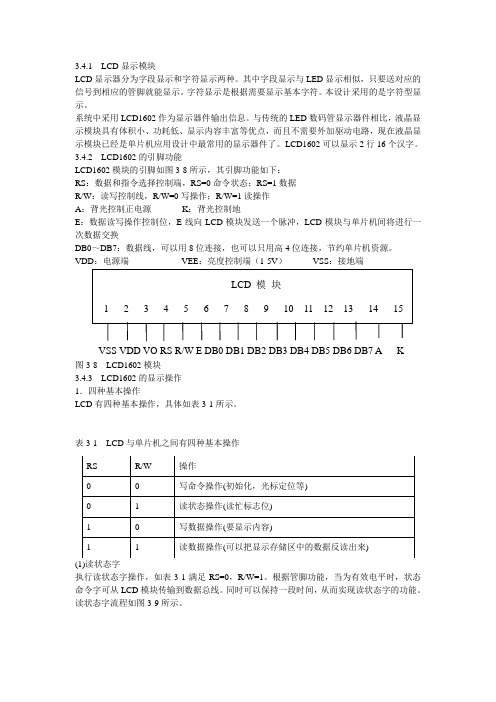
3.4.2LCD1602的引脚功能LCD1602模块的引脚如图3-8所示,其引脚功能如下:RS:数据和指令选择控制端,RS=0命令状态;RS=1数据R/W:读写控制线,R/W=0写操作;R/W=1读操作A:背光控制正电源K:背光控制地E:数据读写操作控制位,E线向LCD模块发送一个脉冲,LCD模块与单片机间将进行一次数据交换DB0~DB7:数据线,可以用8位连接,也可以只用高4位连接,节约单片机资源。
VDD:电源端VEE:亮度控制端(1-5V)VSS:接地端图3-8LCD1602模块3.4.3LCD1602的显示操作1.四种基本操作LCD有四种基本操作,具体如表3-1所示。
表3-1LCD与单片机之间有四种基本操作(1)读状态字执行读状态字操作,如表3-1满足RS=0,R/W=1。
根据管脚功能,当为有效电平时,状态命令字可从LCD模块传输到数据总线。
同时可以保持一段时间,从而实现读状态字的功能。
读状态字流程如图3-9所示。
图3-9读入状态字流程图(2)命令字表3-2所示为命令字,其主要介绍了指令名称、控制信号及控制代码。
其指令名称是指要实现的功能;控制代号是采用的十六进制的数值表示的。
1)清零操作是指输入某命令字后即能将整个屏幕显示的内容全部清除;2)归home位:将光标送到初始位;其中的*号为任意,高低电平均可;3)输入方式:设光标移动方向并指定整体显示,是否移动。
1602使用说明中文版
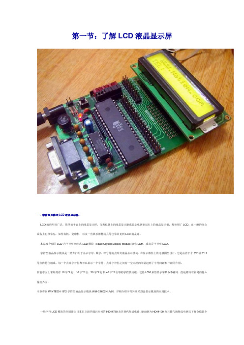
第一节:了解LCD液晶显示屏一:字符型点阵式LCD液晶显示屏:LCD的应用很广泛,简单如手表上的液晶显示屏,仪表仪器上的液晶显示器或者是电脑笔记本上的液晶显示器,都使用了LCD。
在一般的办公设备上也很常见,如传真机,复印机,以及一些娱乐器材玩具等也常常见到LCD的足迹。
本站要介绍的LCD为字符型点阵式LCD模块(liquid Crystal Display Module)简称LCM,或者是字符型LCD。
字符型液晶显示模块是一类专门用于显示字母,数字,符号等的点阵式液晶显示模块。
在显示器件上的电极图型设计,它是由若干个5*7或5*11等点阵符位组成。
每一个点阵字符位都可以显示一个字符。
点阵字符位之间有一空点距的间隔起到了字符间距和行距的作用。
目前市面上常用的有16字*1行,16字*2行,20字*2行和40字*2行等的字符模块组。
这些LCM虽然显示字数各不相同,但是都具有相同的输入输出界面。
本章将以WINTECH 16*2字符型液晶显示模块WM-C1602N为例,详细介绍字符兴高采烈晶显示模块的应用技术。
一般字符LCD模块的控制器为日本日立新华通讯社司的HD44780及其替代集成电路,驱动器为HD44100及其替代的集成电路以下将会略做介绍。
一般初学者由字符型LCD入手比较简单,学完之后,再进一步控制图案型LCD模块。
图1.1所示为16*2地的外观,表1.2为LCM的接脚及功能。
看她的样子在太酷爱,现在我拿她作为讲解实例。
字串8图1.1a:液晶显示模块WM-C1602N背后图1.1b: 液晶显示模块WM-C1602N丰姿图1.1c:液晶显示模块WM-C1602N规格字串4表1.2:液晶显示模块WM-C1602N的接脚及功能应用液晶显示模块WM-C1602N那得先对她的内部结构有所了解,下一节我将会带大家进一步的了解液晶显示模块WM-C1602N。
第二节:LCD液晶显示屏的内部结构液晶显示模块WM-C1602N的内部结构可以分成三部份:一为LCD控制器,二为LCD驱动器,三为LCD显示装置,如图示2.1所示:字串1图2.1:LCM内部方块图字串1目前大多数的LCD液晶显示器的控制器都有采用一颗型号为HD44780的集成电路作控制器。
lcd段码屏驱动原理

lcd段码屏驱动原理
LCD段码屏是一种常见的数字显示设备,它的驱动原理主要涉及到显示控制芯片和显示模块两个方面。
1. 显示控制芯片
LCD段码屏的显示控制芯片通常采用CMOS技术制造,它可以通过内部的控制逻辑和存储器,控制LCD每一段的电压信号,从而实现数字图像的显示。
常见的LCD控制芯片有HD44780、KS0108、KS0066等,其中HD44780是一种具有广泛应用的标准控制芯片。
2. 显示模块
LCD段码屏的显示模块由多个LCD段组成,每个LCD段由数根独立的导电柱和两根金属屏蔽板组成,通过在导电柱和金属屏蔽板之间加电压差,实现液晶分子的定向排列,进而改变透射光的相位差,实现数字图像的显示。
在不同的电压条件下,液晶分子的定向状态也不同,对应不同的显示状态。
因此,通过控制每一段的电压信号,就可以实现数字图像的显示。
总结:
LCD段码屏的驱动原理主要包括显示控制芯片和显示模块两个方面。
通过控制每一段的电压信号,就可以实现数字图像的显示。
海量的应用场景,让段码屏成为了数字显示的中坚力量。
LCM基础知识介绍
对液晶显示用的背光源应该具有:
1、亮度均匀一致,能形成均匀的面光源. 2、亮度高,并可调亮度范围. 3、平板、薄型、适于装配. 4 、重量轻. 5 、光色悦目、基色准确、对液晶显示器件有较好的透过能力. 6 、功耗低,效率高. 7 、成本低. 目前在实际中用作背光源的主要是: A 、小型设备上多用LED. B 、便携及面积稍大时选用EL. C 、当面积较大或需彩色显示时则多用CCFL.
液晶显示模块
液晶显示模块是一种将液晶显示器件、连接件、集成电路、 PCB线路板、背光源、结构件装配在一起的组件.英文名称 叫“LCD Module”,简称“LCM”,中文一般称为“液晶显示 模块”。实际上它是一种商品化的部件.根据我国有关国家 标准的规定:只有不可拆分的一体化部件才称为“模块”, 可拆分的叫作“组件”。所以规范的叫法应称为“液晶显示 组件”。但是由于长期以来人们都已习惯称其为“模块”。 液晶显示器件是一种高新技术的基础元器件,虽然其应用巳 很广泛,但对很多人来说,使用、装配时仍感到困难。特别 是点阵型液晶显示器件,使用者更是会感到无从下手.特殊 的连接方式和所需的专用设备也非人人了解和具备,故此液 晶显示器件的用户希望有人代劳,将液晶显示器件与控制、 驱动集成电路装在一起,形成一个功能部件,用户只需用传 统工艺即可将其装配成一个整机系统。
COB
TAB
COG
是英文“Chip On Glass”的缩写。即芯片 被直接邦定在玻璃上。这种安装方式可 大大减小整个LCD模块的体积,且易于 大批量生产,适用于消费类电子产品用 的LCD,如:手机、PDA等便携式电子 产品。这种安装方式在IC生产商的推动 下,将会是今后IC与LCD的主要连接方 式。
基于STM32的LCD操作

基于STM32的LCD操作STM32的LCD操作是通过使用外部的液晶显示器(Liquid Crystal Display,简称LCD)模块来实现的。
以下是一个基于STM32的LCD操作的详细解释,包括液晶显示器的初始化、数据和命令的发送、以及常用的LCD操作函数。
LCD初始化:1.首先,配置GPIO引脚用于连接到LCD模块的数据线和控制线。
3.然后,发送各种初始化命令,如清除显示、设置光标等。
数据和命令的发送:1.向LCD发送数据(字符或图形数据)时,需要确保LCD处于数据接收状态,而不是指令接收状态。
通常需要在发送数据之前发送一个命令来设置LCD的模式为数据接收模式。
2.通过配置GPIO引脚的电平来发送数据或命令。
常用的LCD操作函数:1. `lcd_init(`: 初始化LCD模块。
2. `lcd_cmd(uint8_t cmd)`: 向LCD发送一个命令。
3. `lcd_data(uint8_t data)`: 向LCD发送一个数据。
4. `lcd_clear(`: 清除LCD显示内容。
5. `lcd_set_cursor(uint8_t row, uint8_t col)`: 设置LCD显示的光标位置。
6. `lcd_print(char *str)`: 在LCD上打印一个字符串。
7. `lcd_create_custom_char(uint8_t location, uint8_t *data)`: 创建自定义字符。
8. `lcd_display_on(`: 打开LCD显示。
9. `lcd_display_off(`: 关闭LCD显示。
上述函数只是基本的示例,具体的函数实现会因不同的液晶模块而有所不同。
在编写代码时,需要根据液晶模块的规格和数据手册来设置相应的GPIO引脚和参数。
总之,基于STM32的LCD操作涉及到GPIO引脚的配置、LCD控制器的初始化、发送数据和命令等步骤。
通过熟悉液晶模块的规格和使用相关的库函数,可以实现对LCD模块的控制。
LCD16032B 液晶显示模块产品说明书
LCM16032B使用说明书目 录序号 内 容 标 题 页码1 概述 22 字符型模块的特点 23 外形及接口引脚功能 2~34 基本原理 45 技术参数 46 时序特性 5~67 指令功能及硬件接口 6~101.概述方便、带中文字库、显示清晰,广泛应用于各种人机交流面板。
LCM16032B 液晶显示模块是160×32 点阵的汉字图形型液晶显示模块,可显示汉字及 图形,内置8192 个中文汉字(16X16 点阵)、128 个字符(8X16 点阵)及 64X256点阵显示RAM (GDRAM )。
可与CPU 直接接口,提供两种界面来连接 微处理机:8-位并行及串行两种连接方式。
具有多种功能:光标显示、画 面移位、睡眠模式等。
1.1结构牢:带PCB、背光、铁框1.2 IC 采用矽创公司ST7920,功能强大,稳定性好1.3功耗低:10 - 100mW(不带背光10mW,带背光不大于100mW); 1.4显示内容:●160*32点阵单色图片;●内置8192 个中文汉字(16X16 点阵)、128 个字符(8X16 点阵)及64X256点阵显示RAM (GDRAM ).1.5指令功能强:可组合成各种输入、显示、移位方式以满足不同的要求;1.6接口简单方便:采用3线SPI 串行接口,可只需3位MPU 的端口。
也可选用8位并行接口。
1.7工作温度宽:-20℃ - 70℃;1.8可靠性高:寿命为50,000小时(25℃)。
3.外形尺寸及接口引脚功能图1.外形尺寸我司专注于液晶屏及液晶模块的研发、制造。
所生产LCM16032B型液晶模块由于使用2.LC M 16032B图像型点阵液晶模块的特性模块的接口引脚功能引脚 符 号 名 称 功 能1 VSS接地 0V2 VDD 电路电源 5V,或3.3V 可选3 V0 LCD V0电压输入 可以通过此脚对LCD 驱动电压进行调整4RS(CS*)寄存器选择信号(串行时为片选:CS)1. 并行接口时:1:数据寄存器 0:指令寄存器2. 串行接口时:片选信号,低电平有效5 R/W(SID*) 读写选择(串行时为串行数据:SID) 1.并行接口时:0: 写 1:读2.串行时为串行数据输入:SID 6E(SCLK*)读写使能信号(串行时为串行时钟:SCLK) 1. 并行接口时:读写使能信号 2. 串行时为串行时钟:SCLK 7~14 D0~D7数据DB0~DB7并行接口时:数据总线DB0~DB7 串行接口时:无效,空脚4位并行接口时,DB4~DB7作为数据总线,DB0~DB3不起作用15 PSB 并行/串行选择 1:选择并行,0:选择串行,也可在PCB 上与VDD(1)或VSS(0)连接达到选择并/串接口。
凤凰显示国际有限公司 22.8英寸240 3200分辨率RGB LCD 模块产品说明书

REVISION RECORDT S REMARKST ENT E CONREV NO. REV DAV1 2015-09-20First Release PreliminaryCONTENTSGENERAL INFORMATIONEXTERNAL DIMENSIONSABSOLUTE MAXIMUM RATINGSELECTRICAL CHARACTERISTICSBACKLIGHT CHARACTERISTICSELECTRO-OPTICAL CHARACTERISTICS INTERFACE DESCRIPTIONREFERENCE APPLICATION CIRCUITRELIABILITY TEST CONDITIONSINSPECTION CRITERIONPRECAUTIONS FOR USING LCD MODULES PACKING SPECIFICATIONPRIOR CONSULT MATTERFACTORY CONTACT INFORMATIONGENERAL INFORMATIONItem of general information Contents Unit LCD type TFT/TRANSFLECTIVE / Recommended Viewing Direction 3:00 O’ Clock Module area (W × H×T) 50.00×69.20×2.85 mm3 Viewing area (W×H) 47.00×60.10 mm2 Active area (W×H) 43.20×57.60 mm2 Number of Dots 240RGB×320 / Pixel pitch (W × H) 0.180×0.180 mm2 Driver IC R61505W / Interface Type Parallel /Serial interface / Input voltage 3.3 V Module Power consumption 225 mw Backlight Type LED /ABSOLUTE MAXIMUM RATINGSParameter of absolutemaximum ratings Symbol Min Max UnitSupply voltage for logic VCC/VCI/IOVCC -0.3 4.6 V Input voltage VIN -0.3 IOVCC+0.3 V Operating temperature Top -20 70 °C Storage temperature TST -30 80 °C Humidity RH - 90%(Max60 °C) RHELECTRICAL CHARACTERISTICSDC CHARACTERISTICSParameter of DCcharacteristicsSymbol Min T yp Max UnitSupply voltage for logic VCC/VCI 2.5 - 3.3 V I/O power supply IOVCC 1.65 - 3.3 V Input Current Idd - 7.8 11.7 mA Input voltage 'H' level V I H 0.8I OVCC - I OVCC V Input voltage 'L' level V I L -0.3 - 0.2I OVCC V Output voltage 'H' level VOH 0.8IOVCC - - V Output voltage 'L' level VOL - - 0.2IOVCC VBACKLIGHT CHARACTERISTICSItem of backlightcharacteristicsSymbol Min. T yp. Max. Unit ConditionForward voltage Vf 2.9 3.2 3.4 V Luminance Lv 3500 3900 4300 cd/m 2If=60mA Ta=25 Number of LED - - 4 - Piece - Connection mode P - Parallel - - - Using condition: constant current driving method If=60mA(+/-10%).ELECTRO-OPTICAL CHARACTERISTICSItem of electro-optical characteristics Symbol Condition Min T yp Max Unit Remark Note Response time Tr+ Tf - 25 40 ms Fig.1 4 Contrast ratio Cr 3467----FIG 2.1Luminance uniformity δ WHITE 70 85 - % F I G 2. 3 Surface LuminanceLvθ=0° ∅=0° Ta=25112 150 -cd/m 2 FI G 2. 2 ∅ = 90°30 45 - deg F I G 3. ∅ = 270°10 20 - deg F I G 3. ∅ = 0°40 50 - deg F I G 3. Viewing angle range θ∅ = 180°20 30 - deg F I G 3. 6 NTSC ratio --- --- - 40 - % - -Red x 0.5087 0.5587 0.6087 - Red y 0.2934 0.3434 0.3934 - Green x 0.2805 0.3305 0.3805 -Green y 0.5208 0.5708 0.6208 -Blue x 0.1157 0.1657 0.2157 -Blue y 0.0930 0.1430 0.1930 - White x 0.2447 0.3047 0.3647 - C I E (x, y) chromaticity White y θ=0°∅=0°Ta=250.2765 0.3365 0.3965 -FIG 2. 5 Note1. Contrast Ratio(CR) is defined mathematically by the following formula. For moreinformation see FIG 2.:Average Surface Luminance with all white pixels(P 1,P2, P 3,P4, P5)Average Surface Luminance with all black pixels (P1, P2, P 3,P4, P5)Note2. Surface luminance is the LCD surface from thesurface with all pixels displaying white. For more information see FIG 2. Lv = Average Surface Luminance with all white pixels (P1, P2, P 3,P4, P5)Note3. The uniformity in surface luminance δ WHITEis determined by measuring luminance at each test position 1 through 5, and then dividing the maximum luminance of 5 points luminance by minimum luminance of 5 points luminance. Formore information see FIG 2. Minimum Surface Luminance with all white pixels (P 1, P 2, P 3,P 4, P 5)Maximum Surface Luminance with all white pixels (P 1, P 2, P 3,P 4, P 5) Note4. Response time is the timerequired for the display to transition from White to black(Rise Time, Tr) and from black to white(Decay Time, Tf). For additional information see FIG 1..Note5. CIE (x, y) chromaticity ,The x,y value is determined by screen active area position 5. Formore information see FIG 2. Note6. Viewing angle is the angle at which the contrast ratio is greater than 2. For TFT module theconrast ratio is greater than 10. The angles are determined for the horizontal or x axis and thevertical or y axis with respect to the z axis which is normal to the LCD surface. For more information see FIG 3.Note7. For Viewing angle and response time testing, the testing data is base on Autronic-Melchers ’sConoScope. Series Instruments. For contrast ratio, Surface Luminance, Luminance uniformity andCIE the testing data is base on TOPCON’s BM-5 photo detector. Note8. For TFT transmissive module,Gray scale reverse occurs in the direction of panel viewing angle.Contrast Ratio = δ WHITE =FIG.1.The definition of Response TimeFIG.2. Measuring method for Contrast ratio,surface luminance, Luminance uniformity,CIE (x,y) chromaticityFIG.3. The definition of viewing angleA : 5 mmB : 5 mmH,V : Active AreaLight spot size ∅=5mm, 500mm distance from the LCD surface to detector lensmeasurement instrument is TOPCON’s luminance meter BM-5INTERFACE DESCRIPTIONInterfaceNO.SymbolI/O or connect toDescriptionWhen not in use1 LEDA LED driver LED ANODE open2 LEDK1 LED driver LED CATHODE open3 LEDK2 LED driver LED CATHODE open4 LEDK3 LED driver LED CATHODE open5 LEDK4 LED driver LED CATHODE open6 I M07 I M18 I M29 I M3I Interface mode Select.Refer to NOTE 1-10 /RESET I Host processor Reset signal. The R61505W is initialized when thissignal is at lowlevel. Make sure to execute a power-on reset when turning on powersupply (Amplitude: IOVCC-GND).-11 DB17 12 DB16 13 DB15 14 DB1415 DB1316 DB1217 DB1118 DB1019 DB920 DB821 DB7 22 DB6 23 DB5 24 DB4 25 DB3 26 DB2 27 DB1 28 DB0I/O Host processor 18-bit bi-directional data bus.If not used, please fix this pin at GND level. 8-bit I/F: DB[17:10] are used. 9-bit I/F: DB[17:9] are used.16-bit I/F: DB[17:10] and DB[8:1] are used.18-bit I/F: DB[17:0] are used.18-bit parallel bi-directional data bus for RGB interfaceoperation (Amplitude: IOVCC-GND). 16-bit I/F: DB[17:13] and DB[11:1] are used. 18-bit I/F: DB[17:0] are used. IOVCC or GND 29 SDO O HostprocessorSerial data output (SDO) pin in serial interfaceoperation. The data is outputted on the falling edge of the SCL signal.Amplitude: IOVCC-GNDopen30 SD I IHostprocessor SPI interface input pin.The data is latched on the rising edge of the SCL signal.- 31 RD I Host processor Read strobe signal in 80-system bus interface operationand enables read operation when RDX is low. Amplitude: IOVCC-GNDIOVCC32 WR/SCL IHost processorWrite strobe signal in 80-system bus interface operationand enables write operation when WRX is low.Synchronous clock signal (SCL) in serial interfaceoperation. Amplitude: IOVCC-GNDIOVCC33 RS IHostprocessor A register select signal.Low: select an index or status registerHigh: select a control registerIOVCC 34 CS IHostprocessor Chip select signal. Amplitude: IOVCC-GNDLow: the R61505W is selected and accessibleHigh: the R61505W is not selected and not accessible. IOVCC 35 FMARK OHostprocessor Frame head pulse signal, which is used when writingdata to the internal frame memory. (Amplitude: IOVCC-GND).open 36 I OVCCPowersupply Power supply for digital O.Connect to an externalpower supply of 1.65 ~ 3.3V .-37 VCCPowersupply Power supply to internal logic regulator circuit.38 VC IPowersupply Power supply for analog circuit..Connect to an externalpower supply of 2.5 ~ 3.3V . -39 GNDPowersupplyInternal logic GND. - 40 NC NCNC-NOTE 1REFERENCE APPLICATION CIRCUITPlease consult our technical department for detail information.RELIABILITY TEST CONDITIONSNo. Test Item Test Condition Inspection after test 1 HighTemperatureStorage 80!2 /200 hours2 LowTemperatureStorage -30!2 /200 hours3 HighTemperatureOperating 70!2 /120 hours4 LowTemperatureOperating -20!2 /120 hours5 Temperature Cycle storage -20!2 ~25~70!2 "10cycles (30min.) (5min.) (30min.)6 Damp proof Test operating 50 !5 "90%RH/120 hours7 VibrationTest Frequency#10Hz~55Hz~10Hz Amplitude#1.5mm, X Y Z direction for total 3hours(Packing condition)8 Droppingtest Drop to the ground from 1m height, one time, every side of carton. (Packing condition)9 ESDtest V oltage:±8KV R: 330Ω C: 150pFAir discharge, 10timeI nspection after2~4hours storage atroom temperature, thesample shall be free fromdefects:1.Air bubble in the LCD;2.Sealleak;3.Non-display;4.missing segments;5.Glass crack;6.Current I dd is twicehigher than initial value.Remark:1.The test samples should be applied to only one test item.2.Sample size for each test item is 5~10pcs.3.For Damp Proof Test, Pure water(Resistance$10MΩ) should be used.4.I n case of malfunction defect caused by ESD damage, if it would be recovered to normal state after resetting, it would be judged as a good part.5.EL evaluation should be excepted from reliability test with humidity and temperature: Some defects such as black spot/blemish can happen by natural chemical reaction with humidity and Fluorescence EL has.6.Failure Judgment Criterion: Basic Specification, Electrical Characteristic, Mechanical Characteristic, Optical Characteristic.INSPECTION CRITERIONThis specification is made to be used as the standard acceptance/rejection criteria for Normal LCM Products from Phoenix Display International, Inc. .1 Sample planSampling plan according to GB/T2828.1-2003/I SO 2859-1#1999 and ANSI/ASQC Z1.4-1993, normal level 2 and based on:Major defect: AQL 0.65Minor defect: AQL 1.52. Inspection conditionViewing distance for cosmetic inspection is about 30cm with bare eyes, and under an environment of 20~40W light intensity, all directions for inspecting the sample should be within 45°against perpendicular line. (Normal temperature 20∼25°C and normal humidity 60±15%RH).Driving voltageThe V op value from which the most optimal contrast can be obtained near the specified V op in the specification (Within ±0.5V of the typical value at 25°C.).3. Definition of inspection zone in LCD.Zone A: character/Digit areaZone B: viewing area except Zone A (ZoneA+ZoneB=minimum Viewing area)Zone C: Outside viewing area (invisible area after assembly in customer’s product)Fig.1 Inspection zones in an LCD.Note: As a general rule, visual defects in Zone C are permissible, when it is no trouble for quality and assembly of customer’s product.4.Inspection Standard4.1 Major Defect4.1.1 Allfunctional defects1) No display 2) Display abnormally 3) Missing vertical horizontal segment4) Short circuit 5) Back-light no lighting, flickering and abnormal lighting.4.1.2 Missing Missing component 4.1.3Outline dimensionOverall outline dimension beyond the drawing is not allowed.Major4.2 Cosmetic DefectItem NoItems to beinspectedInspection StandardClassification ofdefects4.2.2Cosmetic Criteria (Non-Operating)Criterion Partition No. Defect Judgment1 Spots In accordance with Screen Cosmetic Criteria (Operating) No.1. Minor2 Lines In accordance with Screen Cosmetic Criteria (Operating) No.2. MinorMinor3 Bubbles in polarizerSize : d mm Acceptable Qty in active aread ≤ 0.3Disregard0.3 < d ≤ 1.0 31.0 < d ≤ 1.5 11.5 < d 04 Scratch I n accordance with spots and lines operating cosmetic criteria. When theMinorlight reflects on the panel surface, the scratches are not to be remarkable.density Above defects should be separated more than 30mm each other. Minor5 Allowable6 Coloration Not to be noticeable coloration in the viewing area of the LCD panels.MinorBack-lit type should be judged with back-lit on state only.7 Contamination Not to be noticeable. Minor4.2.3 Cosmetic Criteria (Operating)3 Rubbing lineNot to be noticeable.Minor 4 Allowable density Above defects should be separated more than 10mm each other. Minor 5 Rainbow Not to be noticeable.Minor 6 Dot sizeTo be 95% ∼ 105% of the dot size (Typ.) in drawing.Partial defects of each dot (ex. pin-hole) should be treated as ‘Spot’. (see Screen Cosmetic Criteria (Operating) No.1)Minor7 Uneven brightness (only back-lit type module)Uneven brightness must be BMAX / BMIN ≤ 2- BMAX : Max. value by measure in 5 points - BMIN : Min. value by measure in 5 points Divide active area into 4 vertically and horizontally. Measure 5 points shown in the following figure. MinorNote : (1) Size : d = (long length + short length) / 2 (2) The limit samples for each item have priority. (3) Complex defects are defined item by item, but if the numbers of defects are defined in above table, the total number should not exceed 10.(4) In case of ‘concentration’, even the spots or the lines of ‘disregarded’ size should not allowed. Following three situations should be treated as ‘concentration’. - 7 or over defects in circle of ∅5mm. - 10 or over defects in circle of ∅10mm. - 20 or over defects in circle of ∅20mm.: Measuring pointsPRECAUTIONS FOR USING LCD MODULES1Handing Precautions1.1The display panel is made of glass and polarizer. As glass is fragile. I t tends to become orchipped during handling especially on the edges. Please avoid dropping or jarring. Do notsubject it to a mechanical shock by dropping it or impact.1.2If the display panel is damaged and the liquid crystal substance leaks out, be sure not to get anyin your mouth. If the substance contacts your skin or clothes, wash it off using soap and water.1.3Do not apply excessive force to the display surface or the adjoining areas since this may causethe color tone to vary. Do not touch the display with bare hands. This will stain the display areaand degraded insulation between terminals (some cosmetics are determined to the polarizer).1.4The polarizer covering the display surface of the LCD module is soft and easily scratched.Handle this polarizer carefully. Do not touch, push or rub the exposed polarizers with anythingharder than an HB pencil lead (glass, tweezers, etc.). Do not put or attach anything on thedisplay area to avoid leaving marks on it. Condensation on the surface and contact withterminals due to cold will damage, stain or dirty the polarizer. After products are tested at lowtemperature they must be warmed up in a container before coming in to contact with roomtemperature air.1.5If the display surface becomes contaminated, breathe on the surface and gently wipe it with asoft dry cloth. If it is heavily contaminated, moisten cloth with one of the following solvents - Isopropyl alcohol- Ethyl alcoholDo not scrub hard to avoid damaging the display surface.1.6Solvents other than those above-mentioned may damage the polarizer. Especially, do not usethe following.-WaterKetone--solventsAromaticWipe off saliva or water drops immediately, contact with water over a long period of timemay cause deformation or color fading. Avoid contact with oil and fats.1.7Exercise care to minimize corrosion of the electrode. Corrosion of the electrodes is acceleratedby water droplets, moisture condensation or a current flow in a high-humidity environment.1.8Install the LCD Module by using the mounting holes. When mounting the LCD module makesure it is free of twisting, warping and distortion. In particular, do not forcibly pull or bend theI/O cable or the backlight cable.1.9Do not attempt to disassemble or process the LCD module.1.10NC terminal should be open. Do not connect anything.1.11If the logic circuit power is off, do not apply the input signals.1.12Electro-Static Discharge Control Since this module uses a CMOS LSI, the same carefulattention should be paid to electrostatic discharge as for an ordinary CMOS I C. To preventdestruction of the elements by static electricity, be careful to maintain an optimum workenvironment.- Before removing LCM from its packing case or incorporating it into a set, be sure the module and your body have the same electric potential. Be sure to ground the body whenhandling the LCD modules.- Tools required for assembling, such as soldering irons, must be properly grounded.Make certain the AC power source for the soldering iron does not leak. When using anelectric screwdriver to attach LCM, the screwdriver should be of ground potentiality tominimize as much as possible any transmission of electromagnetic waves produced sparkscoming from the commutator of the motor.- To reduce the amount of static electricity generated, do not conduct assemblingand other work under dry conditions. To reduce the generation of static electricity be careful that the air in the work is not too dry. A relative humidity of 50%-60% is recommended. As far as possible make the electric potential of your work clothes and that of the work bench the ground potential.- The LCD module is coated with a film to protect the display surface. Exercise care when peeling off this protective film since static electricity may be generated.1.13Since LCM has been assembled and adjusted with a high degree of precision, avoid applyingexcessive shocks to the module or making any alterations or modifications to it.- Do not alter, modify or change the shape of the tab on the metal frame.- Do not make extra holes on the printed circuit board, modify its shape or change the positions of components to be attached.- Do not damage or modify the pattern writing on the printed circuit board.- Absolutely do not modify the zebra rubber strip (conductive rubber) or heat seal connector.- Except for soldering the interface, do not make any alterations or modifications with a soldering iron.- Do not drop, bend or twist the LCM.3Storage Precautions3.1When storing the LCD modules, the following precaution are necessary.3.1.1Store them in a sealed polyethylene bag. I f properly sealed, there is no need for thedesiccant.3.1.2Store them in a dark place. Do not expose to sunlight or fluorescent light, keep thetemperature between 0°C and 35°C, and keep the relative humidity between 40%RH and60%RH.3.1.3The polarizer surface should not come in contact with any other objects (We advise you tostore them in the anti-static electricity container in which they were shipped).3.2Others3.2.1Liquid crystals solidify under low temperature (below the storage temperature range)leading to defective orientation or the generation of air bubbles (black or white). Airbubbles may also be generated if the module is subject to a low temperature.3.2.2I f the LCD modules have been operating for a long time showing the same displaypatterns, the display patterns may remain on the screen as ghost images and a slightcontrast irregularity may also appear. A normal operating status can be regained bysuspending use for some time. It should be noted that this phenomenon does not adverselyaffect performance reliability.3.2.3To minimize the performance degradation of the LCD modules resulting from destructioncaused by static electricity etc., exercise care to avoid holding the following sections whenhandling the modules.3.2.3.1- Exposed area of the printed circuit board.3.2.3.2-Terminal electrode sections.4USING LCD MODULES4.1I nstalling LCD ModulesThe hole in the printed circuit board is used to fix LCM as shown in the picture below.Attend to the following items when installing the LCM.4.1.1Cover the surface with a transparent protective plate to protect the polarizer and LC cell.4.1.2When assembling the LCM into other equipment,the spacer to the bit between the LCMand the fitting plate should have enough height to avoid causing stress to the modulesurface,refer to the individual specifications for measurements.The measurementtolerance should be ±0.1mm.4.3Precaution for soldering the LCMManual soldering Machine drag soldering Machine press solderingNo RoHS Product 290°C ~350°C.Time : 3-5S.330°C ~350°C.Speed : 15-17 mm/s.300°C ~330°C.Time : 3-6S.Press: 0.8~1.2MpaRoHS Product 340°C ~370°C.Time : 3-5S.350°C ~370°C.Speed : 15-17 mm/s.330°C ~360°C.Time : 3-6S.Press: 0.8~1.2Mpa4.3.1If soldering flux is used, be sure to remove any remaining flux after finishing to solderingoperation (This does not apply in the case of a non-halogen type of flux). t isrecommended that you protect the LCD surface with a cover during soldering to preventany damage due to flux spatters.4.3.2When soldering the electroluminescent panel and PC board, the panel and board should notbe detached more than three times. This maximum number is determined by thetemperature and time conditions mentioned above, though there may be some variancedepending on the temperature of the soldering iron.4.3.3When remove the electroluminescent panel from the PC board, be sure the solder hascompletely melted, the soldered pad on the PC board could be damaged.4.4Precautions for Operation4.4.1Viewing angle varies with the change of liquid crystal driving voltage(VLCD).AdjustVLCD to show the best contrast.4.4.2It is an indispensable condition to drive LCD's within the specified voltage limit since thehigher voltage then the limit cause the shorter LCD life.An electrochemical reaction dueto direct current causes LCD's undesirable deterioration,so that the use of direct currentdrive should be avoided.4.4.3Response time will be extremely delayed at lower temperature than the operatingtemperature range and on the other hand at higher temperature LCD's show dark color inthem.However those phenomena do not mean malfunction or out of order with LCD's,which will come back in the specified operating temperature.4.4.4If the display area is pushed hard during operation,the display will become abnormal.However, it will return to normal if it is turned off and then back on.4.4.5A slight dew depositing on terminals is a cause for electro-chemical reaction resulting interminal open age under the maximum operating temperature,50%RH or less isrequired.4.4.6Input logic voltage before apply analog high voltage such as LCD driving voltage whenpower on. Remove analog high voltage before logic voltage when power off the module.Input each signal after the positive/negative voltage becomes stable.4.4.7Please keep the temperature within the specified range for use and storage.Polarizationdegradation,bubble generation or polarizer peel-off may occur with high temperature andhigh humidity.4.5Safety4.5.1It is recommended to crush damaged or unnecessary LCDs into pieces and wash them offwith solvents such as acetone and ethanol, which should later be burned.4.5.2If any liquid leaks out of a damaged glass cell and comes in contact with the hands,washoff thoroughly with soap and water.。