红外检测晶圆键合质量系统说明书
混合晶圆键合 evg
混合晶圆键合evg全文共四篇示例,供读者参考第一篇示例:混合晶圆键合技术是一种先进的半导体制程技术,它在集成电路制造中起着至关重要的作用。
EVG作为这一领域的领军企业,不断推动着混合晶圆键合技术的发展和应用。
本文将详细介绍混合晶圆键合技术的原理、优势和应用,以及EVG在该领域的贡献和创新。
一、混合晶圆键合技术的原理混合晶圆键合技术是一种通过键合设备将两个或多个不同材料的晶圆精确连接起来的技术。
在半导体制造工艺中,由于不同材料的特性和功能各异,需要将它们进行键合,以实现多功能元件或器件的制作。
混合晶圆键合技术通过高精度的对准和键合工艺,能够实现不同材料的精确对接,并在接触面形成牢固的连接,从而实现不同功能元件的集成。
混合晶圆键合技术的原理主要包括以下几个步骤:首先是对准,通过键合设备精确调整两个晶圆的位置和方向,使它们能够完美对齐;然后是键合,通过热压或其他键合方式,将两个晶圆的接触面加热并施加压力,形成键合连接;最后是检测,通过各种检测手段对键合后的晶圆进行质量检测,确保连接的牢固性和稳定性。
混合晶圆键合技术相比传统的封装技术和晶圆间连接技术具有许多优势。
混合晶圆键合技术可以实现不同材料的精确连接,能够实现更多功能的集成,提高器件性能和功能;混合晶圆键合技术可以实现高密度的集成,能够在有限空间内实现更多功能元件的布局,提高晶体管密度和功率密度;混合晶圆键合技术具有高效率和高可靠性,能够快速完成键合工艺,并能够在不同环境和工作条件下稳定运行;混合晶圆键合技术还可以实现材料的再利用和回收,减少资源浪费和环境污染。
混合晶圆键合技术在半导体制造领域具有广泛的应用。
在先进的微处理器、存储器、传感器和射频器件制造中,混合晶圆键合技术可以实现不同材料的集成和连接,提高器件性能和功能;在集成光电子器件和MEMS器件制造中,混合晶圆键合技术可以实现材料的精确连接和高密度的集成,提高器件的性能和稳定性;在化合物半导体器件和新型材料器件制造中,混合晶圆键合技术可以实现新材料的集成和应用,推动器件的发展和创新。
poi 晶圆键合
POI晶圆键合一般指的是使用POI作为衬底进行晶圆键合的过程。
POI是一种具有高阻硅基底、中层为氧化物氧化层,顶部是单晶压电材料的材料组合。
这种结构使得POI晶圆键合在射频和微波应用中具有优异性能。
晶圆键合是半导体制造过程中的一种重要技术,主要用于将两个晶圆或芯片连接在一起。
这种技术的主要优点是可以在不改变原有晶圆或芯片结构的情况下,将它们连接在一起形成新的功能。
晶圆键合技术的种类很多,包括直接晶圆键合、阳极晶圆键接、粘合剂晶圆接合、玻璃料晶圆接合、共晶晶圆键接等。
其中,POI 晶圆键接是一种特殊的晶圆键合技术,它利用POI材料的特性,在射频和微波领域具有优异的性能。
在实际的晶圆键合过程中,POI晶圆的制造过程通常包括以下步骤:首先,通过化学和物理方法将POI材料沉积在硅基底上;然后,在POI材料的中间层形成氧化物氧化层;最后,在氧化物氧化层上形成单晶压电膜。
整个过程需要严格控制温度、压力和化学物质的浓度,以确保POI晶圆的质量和性能。
值得注意的是,POI晶圆在制造过程中需要特殊的设备和工艺条件,例如高温、高压、强酸、强碱等环境,因此在实际应用中需要考虑设备的耐久性和稳定性。
总的来说,POI晶圆键接技术是一种在射频和微波半导体领域应用广泛的晶圆键合方法,具有优良的性能和可靠性。
亿毫安电子红外线感测器应用手册说明书
——反射式光中断器——物体侦测应用手册一、简介随着科技进步,各种电子产品自动化程度也跟着提高自动化程度越高的产品,代表也包含了更多的感测元件。
为了避免人眼被环境中各种产品或设备感测时发射的光干扰,所以使用人眼无法察觉的红外线(Infrared;IR)产品做为感测器。
这份应用手册将会介绍如何利用红外线发射元件(Infrared Emitter)及红外线接收元件(Infrared Receiver)作物体侦测应用。
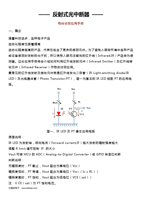
最常见的红外线发射及接收元件就是红外线发光二极管(IR Light-emitting diode;IR LED)及光电晶体管(Photo Transistor;PT),图一为基本的IR LED搭配PT的应用电路。
图一、IR LED及PT基本应用电路原理说明:IR LED为发射端,顺向电流(Forward current;IF)越大发射的辐射强度越大调整R limit值可控制IF的大小Vout可接MCU的ADC(Analog-to-Digital Converter)或GPIO做准位判断判断说明:无辐照度时,PT截止,Vout输出为高电位(Vcc)辐照度低时,PT导通,Vout输出为高电位(Vcc–(Ic x RL))辐照度高时,PT饱和,Vout输出为低电位(VCE(sat))注:V CE(sat)为PT饱和电压。
二、利用反射式ITR做物体侦测方法IR LED通常和PT一起搭配作为物体侦测或是遮断侦测应用图二为利用IR LED发射IR经由物体反射到PT做反射式物体侦测的示意图;为了避免IR LED发射的IR不经过物体反射,直接在机构内照射到PT造成误判,所以IR LED跟PT 必须有效隔离。
利用底下的两项特性,即可做到反射物的距离侦测。
反射物距离越近,PT收到的反射辐照度越强,输出的电流会越高。
不同的材料会有不同的反射率,一般颜色越深、表面越粗糙的物体反射率越低,同距离情况下,接收端输出的电流相对会降低。
晶片测试系统说明书

FEATURES / BENEFITSFlexibilityIdeal for a wide range of applications such as RF, mm-Wave and sub-THz characterization, FA, DWC, MEMS, optoelectronic tests and WLRA stable platen mounted with up to sixteen positioners provides a function similar to a probe card A variety of accessories are available such as laser cutters, platens and chucks for RF, mm-Wave and sub-THz testingStabilitySolid station frameBuilt-in vibration-isolation solution for superior vibration attenuation Rigid microscope bridgeEase of useErgonomic and straightforward design for comfortable and easy operation Low-profile designSimple microscope operationQuick and ergonomic change of DUT through pull-out stageThe MPS150 is a very cost-effective and simple, yet highly-precise manual probe system for wafers and substrates up to 150 mm. It supports a wide variety of applications such as C-V/I-V, RF, mm-Wave and sub-THz measurements, device and wafer characterization tests (DWC), failure analysis (FA), submicron probing, MEMS, optoelectronic engineering tests and more. Its stable platen is designed to accommodate up to sixteen positioners, providing a function similar to a probe card for special wafer-level reliability (WLR) applications.The MPS150 probe system provides a solid, compact and modular platform with integrated vibration-isolation solution and a unique pull-out chuck stage. The station can accommodate application-specific high-planarity-isolated chucks. The height of the solid platen can be adjusted up to 40 mm, allowing quick and easy setup of the system to accommodate any application. The highly-repeatable contact separation of 200 μm ensures excellent contact performance. In addition to the precision platen movement, the chuckprovides precise wafer height alignment up to 10 mm and chuck stroke up to 3 mm. In addition, the rigid microscope bridge enhances contact stability and contact performance.The modular design of the MPS150 allows you to mount a microscope of your choice, enabling you to upgrade the system from the simplest probing platform with a manual microscope to a highly-sophisticated probing platform with a programmable microscope, or to a wafer-level MEMS test system by simply adding a non-contact vibration analyzer.MPS150150 mm Manual Probe SystemDATA SHEETMECHANICAL PERFORMANCEChuck StageTravel155 mm x 155 mm (6 in. x 6 in.)Resolution 5 µmPlanarity over 150 mm (6 inch)< 10 µmLoad stroke, Y axis90 mmZ height adjustment range10 mmZ contact / separation / load stroke0-3 mm adjustableTheta travel (standard)360°Theta travel (fine)± 8°Theta resolution7.5 x 10-3 gradientManual Microscope Stage (On Bridge)Travel range50 mm x 50 mm (2 in. x 2 in.) / 150 mm x 100 mm (6 in. x 4 in)Resolution≤ 5 µm (0.2 mils)Scope lift Manual, tilt-back or linear pneumaticProgrammable Microscope Stage *Travel range50 mm x 50 mm (2 in. x 2 in.)Resolution0.25 µm (0.01 mils)Scope lift Programmable 130 mm* Electronics box for manual systems (P/N 157-137) requiredPHYSICAL DIMENSIONSStation Platform, with Bridge *Station dimensions588 mm (W) x 638 mm (D) x 654 mm (H) (23 inch x 25 inch x 26 inch)Weight~60 kg (132 lb.)* Station accessories such as cameras and laser cutters may increase the total height to 900 mm (35.4 inch)PLATEN SYSTEMPlatenPlaten space (typical)Universal platen: space for up to four DPP2xx/DPP3xx/DPP4xx/RPP210 or up to twelve DPP105positionersUniversal platen with optional probe card adapter: space for up to eight DPP2xx/DPP3xx/DPP4xx/RPP210 or up to sixteen DPP105 positionersMMW platen: space for up to four RPP305 or two LAP positionersZ-Height adjustment range Maximum 40 mm (depending on configuration)Minimum platen-to-chuck height 16 mm (universal platen)Separation lift 200 µmSeparation repeatability < 1 µmVertical rigidity / force 5 µm / 10 N (0.2 mils / 2.2 lb.)Accessory mounting options Universal platen: magnetic, vacuumRF-platen: bolt-down, magneticPHYSICAL DIMENSIONSStandard Wafer ChuckDiameter 150 mmMaterial Stainless steelDUT sizes supported Shards or wafers 25 mm (1 in.) through 150 mm (6 in.)Vacuum ring diameter Universal: 4 mm, 7 mm, 22 mm, 42 mm, 66 mm, 88 mm, 110 mm, 132 mmStandard: 22 mm, 42 mm, 66 mm, 88 mm, 110 mm, 132 mmVacuum ring actuation Universal: all connected in meander, center hole 1.5 mm diameterStandard: mechanically selected, center hole 1.0 mm diameterChuck surface Planar with centric-engraved vacuum groovesSurface planarity ≤ ± 3 µmRigidity< 15 µm / 10 N @ edgeRF Wafer ChuckDiameter 150 mm with two additional AUX chucksMaterial Stainless steel with HF/OPTO surface (flat with 0.7 mm holes)DUT sizes supported Main: single DUTs down to 3 mm x 5 mm size or wafers 25 mm (1 inch) through 150 mm (6 inch)AUX: up to 18 mm x 26 mm (1 in. x 0.7 inch) eachVacuum hole sections (diameter) 22 mm, 42 mm, 66 mm, 88 mm, 110 mm, 132 mm (four holes in center with 2.5 mm x 4.3 mm distance) Vacuum hole actuation Mechanically selectedChuck surface Planar with 0.7mm diameter holes in centric sectionsSurface planarity ≤ ± 3 µmRigidity< 15 µm / 10N @ edgeTRIAX Wafer ChuckDiameter 150 mm with three additional AUX chucks (two with vacuum fixation)Material Stainless steelDUT sizes supported Main: wafers 50 mm through 150 mmAUX: up to 18 mm x 26 mm (1 inch x 0.7 inch) eachVacuum hole sections (diameter) 50 mm, 100 mm, 150 mm (2 inch, 4 inch, 6 inch)Vacuum hole actuation 3x vacuum switch unitChuck surface Planar with 0.4 mm diameter holes in centric sectionsSurface planarity ≤ ±5 µmNON-THERMAL CHUCKSNote: Results measured with non-thermal chuck at standard probing height (10,000 µm) with chuck in a dry environment. Moisture in the chuck may degrade performance.MPS-CHUCK150-COAXOperation voltage Standard: in accordance with EC 61010, certificates for higher voltages available upon request Isolation* > 2 GΩCapacitance 100 pF100 pF* Factory test with multimeter with maximum 2 GΩ range.NON-THERMAL CHUCKS (CONTINUED)MPS-CHUCK150-TRIAX1In Purged Shield Enclosure Open2 Humidity2< 30%50% Leakage (1 sigma)< 50 fA< 200 fA Leakage (average)NA NA Leakage (P-P)< 100 fA< 1000 fA Resistance (F-G)> 1 TΩ> 1 TΩResistance (G-S)> 1 TΩ> 1 TΩResistance (F-S)> 1 TΩ> 1 TΩResidual capacitance @ 3 pA Tx< 20 pF< 20 pF Capacitance @ 300 pA (F-G)< 400 pF< 400 pF Capacitance @ 300 pA (G-S)< 400 pF< 400 pFTRIAXIAL PROBE ARMS1Standard Triaxal Arm (PN 100525)Advanced Triax Option (PN 157-450 and DCP)In Purged Shield Enclosure In Purged Shield Enclosure Humidity3< 30%< 30%Leakage (1 sigma)< 5 fA< 2 fAResistance (F-G)> 20 TΩ> 50 TΩResistance (G-S)> 4 TΩNAResidual capacitance @ 3 pA Tx< 1 pF< 0.3 fFCapacitance @ 300 pA (F-G)< 300 pF< 150 pFCapacitance @ 300 pA (G-S)< 400 pF< 200 pFCOAXIAL PROBE ARMS1Coaxial Probe Arm(PN 100561)Open / Ambient 2, 4Resistance (Signal-Shield)> 20 TΩCapacitance (Signal-Shield)< 200 pF1. Test conditions: B1500 with SMU B1517, triax test cables and adapter ground unit (104-337). Resistor test setup: 10 V HR Mode PCL Factor 15. Capacitor test setup: 3 pA / 300 pA HR Mode PCL Factor 4. Leakage test setup: 10 V HR Mode PCL Factor 40.2. Depending on DC-/AC-noise environment.3. Environment data (not specification data).4. Depending on humidity.THERMAL CHUCK PERFORMANCEMPS-TC150-CTX-300C1Triax @ 25°C Triax @ 200°C Triax @ 300°C≥ 500 V ≥ 500 V ≥ 500 VBreakdown voltage2 Force-to-guard≥ 500 V ≥ 500 V ≥ 500 VGuard-to-shield≥ 500 V ≥ 500 V ≥ 500 VForce-to-shield≥ 1 x 10¹²≥ 1 x 10¹¹≥ 5 x 10⁹Resistance3Force-to-guardGuard-to-shield≥ 1 x 10¹¹≥ 1 x 10¹⁰≥ 1 x 10⁹≥ 5 x 10¹²≥ 2 x 10¹¹≥ 5 x 10⁹Force-to-shieldChuck leakage4≤ 100 fA ≤ 10 pA ≤ 300 pAResidual capacitance ≤ 50 pFSettling time6@ 10 V 50 fA 500 ms (typical)MPS-TC150-CTX-300C (using coax-triax adapter)1, 5Coax@25°C Coax @200°C Coax @300°CBreakdown voltage2≥ 500 V ≥ 500 V ≥ 500 V≥ 1 x 10¹²≥ 1 x 10¹¹≥ 5 x 10⁹Resistance3Signal-to-shieldChuck leakage4≤ 600 fA ≤ 15 pA ≤ 1 nAResidual capacitance ≤ 600 pFMPS-TC150-RF-300C1, 5Coax@25°C Coax @200°C Coax @300°CBreakdown voltage2≥ 500 V ≥ 500 V ≥ 500 VResistance3≥ 1 x 10¹²≥ 1 x 10¹¹≥ 5 x 10⁹Chuck leakage4≤ 600 fA ≤ 15 pA ≤ 1 nAResidual capacitance ≤ 600 pF1. Performance values determined using EMV shielded chamber. Actual value depend on electromagnatic surrounding and shielding situation of the probe station.2. For fully-baked chuck: 90°C for 60 minutes + 200°C for 240 minutes + 300°C for 480 minutes.3. For fully-baked chuck: 90°C for 60 minutes + 200°C for 240 minutes + 300°C for 480 minutes; controller on; 21-23C° environment with ≤ 50% humidity.4. Overall leakage current is comprised of two separate components: 1) offset, and 2) noise. Offset is the DC value of current due to instrument voltage offset driving through isolation resistance. Noise is low frequency ripple superimposed on top of offset and is due to disturbances in the probe station environment.Noise and leakage are measured with a 4156C NOISE.dat CMI program or equivalent; 4ms sample rate, auto scale, 1nA compliance, 1 NPLC integration.5. Chuck: Guard-Shield shorted, B1500: triax, guard open.6. Settling time is measured with a 4156C SETLB.dat CMI program or equivalent; 2 ms sampling rate, limited auto 1 nA, 1 μA compliance, 3 NPLC integration. Transition TimeCoolingHeating25°C to 100°C° 100°C to 200°C 200°C to 300°C 300°C to 200°C 200°C to 100°C 100°C to 25°C MPS-TC150-CTX-300C 145 sec 155 sec 300 sec 145 sec 245 sec 1525 secMPS-TC150-RF-300C 180 sec 300 sec 540 sec 165 sec 310 sec 1650 secMPS-TC150-CTX-300C and MPS-TC150-RF-300C SpecificationsTemperature range + 30°C to 300°CTemperature accuracy ± 0.1°C (with calibrated controller)Temperature resolution 0.1°CTemperature uniformity ≤ 0.5°C @ 30°C, ≤ 3.0°C @ 300°CChuck flatness ≤ 30 μm (0.12 mils) @ +30°C to 300°CAudible noise < 58 dBSupply voltage 100/230 VAC 50/60 HzSupply air 350 liters/min (12.4 SCFM)Power consumption 530 VA (typical)Dimensions 300 mm (W) x 360 mm (D) x 135 mm (H) (11.8 in. x 14.2 in. x 5.3 in.)Weight 12 kg (26.5 lb.)FACILITY REQUIREMENTSPower Base machine (without accessories and thermal chuck*): Not required Vacuum -0.8 bar Compressed air4 bar*See Probe Station Accessory Catalog for power requirements for accessories and ERS AirCool3 Facility Planning Guide for power requirements for thermal chucks.ORDERING INFORMATIONMPS150-based Application-dedicated Pre-configured Packages Part Number DescriptionEPS150COAX 150 mm manual probing solution for DC parametric testEPS150COAXPLUS 150 mm manual probing solution for DC parametric test (including platen lift)EPS150TRIAX 150 mm manual probing solution for low-noise measurements EPS150RF 150 mm manual probing solution for RF applicationsEPS150MMW 150 mm manual probing solution for mmW, THz and load pull applications EPS150FA150 mm manual probing solution for failure analysisREGULATORY COMPLIANCECertificationCE, cNRTLus, CBWARRANTYWarranty* Fifteen months from date of delivery or twelve months from date of installation Service contractsSingle and multi-year programs available to suit your needs*See Cascade Microtech’s Terms and Conditions of Sale for more details.MPS150-DS-0215© Copyright 2015 Cascade Microtech, Inc.All rights reserved. Cascade Microtech is a registeredtrademark of Cascade Microtech, Inc. All other trademarks are the property of their respective owners.Data subject to change without noticeCascade Microtech, Inc.Corporate Headquarters toll free: +1-800-550-3279phone: +1-503-601-1000email: cmi_sales @Germanyphone: +49-89-9090195-0email: cmg_sales @Japanphone: +81-3-5615-5150email: cmj_sales @Chinaphone: +86-21-3330-3188email: cmc_sales @Singaporephone: +65-6873-7482email: cms_sales @ Taiwanphone: +886-3-5722810email: cmt_sales @。
- 1、下载文档前请自行甄别文档内容的完整性,平台不提供额外的编辑、内容补充、找答案等附加服务。
- 2、"仅部分预览"的文档,不可在线预览部分如存在完整性等问题,可反馈申请退款(可完整预览的文档不适用该条件!)。
- 3、如文档侵犯您的权益,请联系客服反馈,我们会尽快为您处理(人工客服工作时间:9:00-18:30)。
红外检测晶圆键合质量系统说明书
⏹概述
该系统是用于晶圆键合过程后的质量检测系统。
能够提供给使用者快速、精确的无损界面检测图像。
该系统具有很强的通用性,不仅适用于硅-硅、玻璃-硅或者玻璃-玻璃晶圆键合,还适用于GaAs、InP等半导体晶圆。
该系统克服了X射线投射法和扫面声学显微探测法费时费力、系统复杂和成本昂贵的特点。
最大能检测的晶圆直径为200mm,满足绝大多数科研和生产所需。
该系统具有高效、实时、无损、低成本、结果清晰的特点,是实时检测空洞和键合过程的理想手段。
⏹特点
1.红外光源以提供高的检测质量
2.键合晶圆对的自动成像
3.高灵敏度CCD以提供高分辨率、高对比度图像
4.微米级的检测精度
5.可检测的最大晶圆直径为200mm
6.搭载不同波长的滤波片可以检测绝大多数的晶圆材料
7.基于计算机的图像获取软件
8.支持Windows/Linux系统,集成多种二次开发工具
⏹工作原理
待检测圆片
白炽灯
图1 检测系统结构图
对于理想晶体来说,光是否透射晶体取决于光子的能量和晶体材料的禁带宽度: g E hc />λ
对于硅的禁带宽度为1.12eV ,故其透射光最小波长为1.1μm 。
如果两片晶圆的键合界面存在未键合区域,则入射光在上下表面两次反射后形成相干光,经红外摄像机处理后,会在显示器上出现明暗交替的干涉条纹。
如果未键合区域面积较大且间隙高度不大,则会出现很多较大的干涉条纹;当键合界面处间隙较大时,入射光无法形成干涉现象,在图片上的对应位置将只能出现颜色较暗的图案。
因此,根据键合片的红外透射图像,就可以检测到键合圆片的缺陷状态及分布。
根据干涉的圈数还可以定量的计算出空洞的大小。
产生暗条纹,应满足:
λλ21212+=m nd ),2,1,0( =m
其中n 为空洞中介质的折射率,d 为空洞高度,m 为干涉环数,λ为所用红外光的波长。
若已知n 、m 、λ,则可得:
n n m d 44λλ+= ),2,1,0( =m
图2 未键合区域光线反射图图3 红外透射干涉图
检测系统主要有四个部分:光源部分、工作台部分、红外相机部分和计算机部分。
测试系统的结构如图1所示,主要部分包括:底座、盒体、白炽灯、匀光片、待检测圆片、滤光片、放大镜头和红外摄像机。
不同尺寸的晶圆成像距离不同,镜头和晶圆间距离的调节可以通过改变横梁的高度和改变摄像机的焦距来实现。
盒体设计如图4所示。
采用4光源,以获得较为均匀一致的光强分布,避免不均匀光强对观测结果的影响。
为了获得较高对比度的图像和适应不同尺寸晶圆的成像,通常需要调节功率调节器以使照明系统提供的光强可控制。
低光强的图像对比度较高,而高光强的图像分辨率更高。
图4 盒体结构图图5 检测系统实物图
技术指标
(此文档部分内容来源于网络,如有侵权请告知删除,文档可自行编辑修改内容,
供参考,感谢您的支持)。