Maxim双通道偏置控制器MAX1385-6-11008
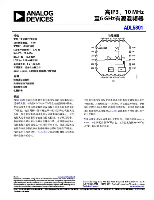
ADL5801中文资料
ADI中文版数据手册是英文版数据手册的译文,敬请谅解翻译中可能存在的语言组织或翻译错误,ADI不对翻译中存在的差异或由此产生的错误负责。如需确认任何词语的准确性,请参考ADI提供 的最新英文版数据手册。
ADL5801 目录
特性 .................................................................................................. 1 应用 .................................................................................................. 1 功能框图 ......................................................................................... 1 概述 .................................................................................................. 1 修订历史 ......................................................................................... 2 技术规格 ......................................................................................... 3 绝对最大额定值 ............................................................................ 6 ESD警告 ..................................................................................... 6 引脚配置和功能描述 ................................................................... 7 典型工作特性 ................................................................................ 8 采用宽带巴伦的下变频器模式 ............................................ 8 采用Mini-Circuits® TC1-1-43M+ 输入巴伦的下变频器模式 ................................................... 12 采用Johanson 3.5 GHz输入巴伦的下变频器模式 ......... 14 采用Johanson 5.7 GHz输入巴伦的下变频器模式 ......... 16 900 MHz输出匹配下的上变频器模式 .............................. 18 2.1 GHz输出匹配下的上变频器模式 ................................ 20 杂散性能 .................................................................................. 23 电路描述 ....................................................................................... 27 LO放大器和分路器 ............................................................... 27 RF电压电流(V-I)转换器....................................................... 27 混频器内核 ............................................................................. 27 混频器输出负载..................................................................... 27 RF检波器 ................................................................................. 28 偏置电路 .................................................................................. 28 应用信息 ....................................................................................... 31 基本连接 .................................................................................. 31 RF和LO端口 ........................................................................... 31 IF端口 ....................................................................................... 32 下变频至低频 ......................................................................... 33 宽带操作 .................................................................................. 34 RF和LO输入的单端驱动...................................................... 36 评估板 ........................................................................................... 38 外形尺寸 ....................................................................................... 40 订购指南 .................................................................................. 40
MAX4460中文资料
General DescriptionThe MAX4460/MAX4461/MAX4462 are instrumentation amplifiers with precision specifications, low-power con-sumption, and excellent gain-bandwidth product.Proprietary design techniques allow ground-sensing capability combined with ultra-low input current and increased common-mode rejection performance. These Rail-to-Rail ®output instrumentation amplifiers are offered in fixed or adjustable gains and the option for either a shutdown mode or a pin to set the output voltage relative to an external reference (see Ordering Information and Selector Guide ).The MAX4460 has an adjustable gain and uses ground as its reference voltage. The MAX4461 is offered in fixed gains of 1, 10, and 100, uses ground as its reference volt-age, and has a logic-controlled shutdown input. The MAX4462 is offered in fixed gains of 1, 10, and 100 and has a reference input pin (REF). REF sets the output volt-age for zero differential input to allow bipolar signals in single-supply applications.The MAX4460/MAX4461/MAX4462 have high-impedance inputs optimized for small-signal differential voltages. The MAX4461/MAX4462 are factory trimmed to gains of 1, 10,or 100 (suffixed U, T, and H) with ±0.1% accuracy. The typical offset of the MAX4460/MAX4461/MAX4462 is 100µV. All devices have a gain-bandwidth product of 2.5MHz.These amplifiers operate with a single-supply voltage from 2.85V to 5.25V and with a quiescent current of only 700µA (less than 1µA in shutdown for the MAX4461). The MAX4462 can also be operated with dual supplies.Smaller than most competitors, the MAX4460/MAX4461/MAX4462 are available in space-saving 6-pin SOT23 packages.________________________ApplicationsIndustrial Process Control Strain-Gauge Amplifiers Transducer InterfacePrecision Low-Side Current Sense Low-Noise Microphone Preamplifier Differential Voltage Amplification Battery-Powered Medical EquipmentFeatureso Tiny 6-Pin SOT23 Package o Input Negative Rail Sensing o 1pA (typ) Input Bias Current o 100µV Input Offset Voltage o Rail-to-Rail Outputo 2.85V to 5.25V Single Supply o 700µA Supply Current o ±0.1% Gain Erroro 2.5MHz Gain-Bandwidth Product o 18nV/√Hz Input-Referred NoiseMAX4460/MAX4461/MAX4462SOT23, 3V/5V , Single-Supply, Rail-to-RailInstrumentation Amplifiers________________________________________________________________Maxim Integrated Products119-2279; Rev 2; 11/02For pricing, delivery, and ordering information,please contact Maxim/Dallas Direct!at 1-888-629-4642, or visit Maxim’s website at .Ordering InformationRail-to-Rail is a registered trademark of Nippon Motorola, Ltd.Pin Configurations appear at end of data sheet.Typical Application CircuitsSelector Guide appears at end of data sheet.M A X 4460/M A X 4461/M A X 4462SOT23, 3V/5V , Single-Supply, Rail-to-Rail Instrumentation Amplifiers 2_______________________________________________________________________________________ABSOLUTE MAXIMUM RATINGSStresses beyond those listed under “Absolute Maximum Ratings” may cause permanent damage to the device. These are stress ratings only, and functional operation of the device at these or any other conditions beyond those indicated in the operational sections of the specifications is not implied. Exposure to absolute maximum rating conditions for extended periods may affect device reliability.Supply Voltage (V DD to V SS ) ...................................-0.3V to +6V All Other Pins...................................(V SS - 0.3V) to (V DD + 0.3V)Output Short-Circuit Duration to Either Supply.........................1s Continuous Power Dissipation (T A = +70°C)6-Pin SOT23 (derate 8.7mW/°C above +70°C)............695mW 8-Pin SO (derate 5.9mW/°C above +70°C)..................470mWOperating Temperature Range ...........................-40°C to +85°C Junction Temperature......................................................+150°C Storage Temperature Range.............................-65°C to +150°C Lead Temperature (soldering, 10s)....................................300°CELECTRICAL CHARACTERISTICS—MAX4460/MAX4461(V DD = 5V, V CM = 0V, V DIFF = V IN+- V IN-= 50mV to 100mV for G = 1, 20mV to 100mV for G = 10, 2mV to 48mV for G =100,MAX4460 is configured for G = 10, R L = 200k Ωto GND, T A = +25°C , unless otherwise noted.)MAX4460/MAX4461/MAX4462SOT23, 3V/5V , Single-Supply, Rail-to-RailInstrumentation AmplifiersELECTRICAL CHARACTERISTICS —MAX4460/MAX4461 (continued)ELECTRICAL CHARACTERISTICS —MAX4460/MAX4461M A X 4460/M A X 4461/M A X 4462SOT23, 3V/5V , Single-Supply, Rail-to-Rail Instrumentation Amplifiers 4_______________________________________________________________________________________ELECTRICAL CHARACTERISTICS —MAX4460/MAX4461 (continued)(V DD = 5V, V CM = 0V, V DIFF = V IN+- V IN-= 50mV to 100mV for G = 1, 20mV to 100mV for G = 10, 2mV to 48mV for G = 100,MAX4460 is configured for G = 10, R L = 200k Ωto GND, T A = T MIN to T MAX , unless otherwise noted.)MAX4460/MAX4461/MAX4462SOT23, 3V/5V , Single-Supply, Rail-to-RailInstrumentation Amplifiers_______________________________________________________________________________________5ELECTRICAL CHARACTERISTICS —MAX4462(V DD = 5V, V SS = 0V, V CM = V REF = V DD /2, R L = 100k Ωto V DD /2, T A = +25°C , unless otherwise noted. V DIFF = V IN+- V IN-= -100mVM A X 4460/M A X 4461/M A X 4462SOT23, 3V/5V , Single-Supply, Rail-to-Rail Instrumentation Amplifiers 6_______________________________________________________________________________________ELECTRICAL CHARACTERISTICS —MAX4462 (continued)ELECTRICAL CHARACTERISTICS —MAX4462MAX4460/MAX4461/MAX4462SOT23, 3V/5V , Single-Supply, Rail-to-RailInstrumentation Amplifiers_______________________________________________________________________________________7ELECTRICAL CHARACTERISTICS —MAX4462 (continued)Specifications section).Note 2:Guaranteed by design, not production tested.Note 3:Output swing high is measured only on G = 100 devices. Devices with G = 1 and G = 10 have output swing high limited bythe range of V REF , V CM , and V DIFF (see Output Swing section).Note 4:Short-circuit duration limited to 1s (see Absolute Maximum Ratings).Note 5:SOT23 units are 100% production tested at +25°C. Limits over temperature are guaranteed by design.M A X 4460/M A X 4461/M A X 4462SOT23, 3V/5V , Single-Supply, Rail-to-Rail Instrumentation Amplifiers 8_______________________________________________________________________________________Typical Operating Characteristics(V DD = 5V, V SS = 0V, V IN + = V IN-= V REF = V DD /2, R L = 100k Ωto V DD /2, T A = +25°C, unless otherwise noted. V DIFF = V IN+- V IN-= -100mV to +100mV for G = 1 and G = 10, -20mV to +20mV for G = 100.)10,00010001001010.11001101k10k100kINPUT VOLTAGE NOISE vs. FREQUENCYM A X 4460 t o c 07FREQUENCY (Hz)I N P U T V O L T A G E N O I S E (n V /H z )PEAK-TO-PEAK NOISE (0.1Hz TO 10Hz)1s/div2µV/divINPUT REFERRED G = 1, 10, OR 1000.0100.0050.0150.0200.0250.0300.0350.0400.045101001k 10k100kTOTAL HARMONIC DISTORTION PLUS NOISE vs. FREQUENCYFREQUENCY (Hz)T H D + N (%)042108612141618-300-200-150-250-100-5050100150200250300VOLTAGE OFFSET HISTOGRAMVOLTAGE OFFSET (µV)P E R C E N T A G E O F U N I T S42612141081600.020.030.040.050.010.060.070.080.090.10GAIN-LINEARITY HISTOGRAMLINEARITY (%)P E R C E N T A G E O F U N I T S426121410816-5-3-2-10-412345VOLTAGE OFFSET DRIFT HISTOGRAMVOLTAGE OFFSET DRIFT (µV/°C)P E R C E N T A G E O F U N I T S42861012-0.50GAIN ERROR HISTOGRAMGAIN ERROR (%)P E R C E N T A G E O F U N I TS-0.4-0.2-0.10.10.20.30.40.5-0.3-130-120-90-100-110-80-70-60-50-40-30-200.11011001k10kCOMMON-MODE REJECTION RATIOvs. FREQUENCYFREQUENCY (Hz)C M R R (d B )POWER-SUPPLY REJECTION RATIOVS. FREQUENCYFREQUENCY (Hz)0.01101001k 0.1110kP S R R (d B )-120-100-80-60-20-40MAX4460/MAX4461/MAX4462SOT23, 3V/5V , Single-Supply, Rail-to-RailInstrumentation Amplifiers_______________________________________________________________________________________930065040080075070090095085010002.75 3.503.753.003.25 4.004.254.504.755.00SUPPLY CURRENTVS. SUPPLY VOLTAGESUPPLY VOLTAGE (V)S U P P L Y C U R R E N T (µA )60055050045035004286121014SHUTDOWN CURRENT VS. SUPPLY VOLTAGESUPPLY VOLTAGE (V)S U P P L Y C U R R E N T (n A )2.753.503.753.003.254.004.254.504.755.0000.040.020.080.060.120.100.140.180.160.200.20.30.40.10.50.60.70.90.8 1.0MAX4462HNORMALIZED OUTPUT ERROR vs. COMMON-MODE VOLTAGEV CM (V)N O R M A L I Z E D O U T P U T E R R O R (%)-0.30-0.16-0.18-0.20-0.22-0.24-0.26-0.28-0.12-0.14-0.08-0.10-0.06-0.02-0.040-2.7-2.1-1.8-2.4-1.5-1.2-0.9-0.60-0.3MAX4462HNORMALIZED OUTPUT ERROR vs. COMMON-MODE VOLTAGEV CM (V)N O R M A L I Z E D O U T P U T E R R O R (%)040208060120100140180160200023415679810OUTPUT SWING HIGHVS. OUTPUT CURRENTOUTPUT CURRENT (mA)V D D - V O U T (m V )10050200150300250350450400500023*********OUTPUT SWING LOW vs. OUTPUT CURRENTOUTPUT CURRENT (mA)V O U T - V S S (m V )Typical Operating Characteristics (continued)(V DD = 5V, V SS = 0V, V IN + = V IN-= V REF = V DD /2, R L = 100k Ωto V DD /2, T A = +25°C, unless otherwise noted. V DIFF = V IN+- V IN-= -100mV to +100mV for G = 1 and G = 10, -20mV to +20mV for G = 100.)-1010030204050GAIN vs. FREQUENCYFREQUENCY (Hz)G A I N (d B)0.011100.11001k10k 222325242627-4010-15356085GAIN BANDWIDTH vs. TEMPERATURETEMPERATURE (°C)-3d B B A N D W I D T H (k H z )SETTLING TIME (GAIN = 100)MAX4460 toc1840µs/divINPUT 10mV/divOUTPUT 500mV/divOUTPUT 10mV/divM A X 4460/M A X 4461/M A X 4462SOT23, 3V/5V , Single-Supply, Rail-to-Rail Instrumentation Amplifiers 10______________________________________________________________________________________Typical Operating Characteristics (continued)(V DD = 5V, V SS = 0V, V IN + = V IN-= V REF = V DD /2, R L = 100k Ωto V DD /2, T A = +25°C, unless otherwise noted. V DIFF = V IN+- V IN-= -100mV to +100mV for G = 1 and G = 10, -20mV to +20mV for G = 100.)LARGE-SIGNAL PULSE RESPONSE(GAIN = 1V/V)MAX4460 toc19INPUTOUTPUT50mV/div1µs/div LARGE-SIGNAL PULSE RESPONSE(GAIN = 100V/V)MAX4460 toc20INPUT 10mV/divOUTPUT 1V/div20µs/divSMALL-SIGNAL PULSE RESPONSE(GAIN = 1V/V)MAX4460 toc21INPUTOUTPUT10mV/div1µs/divSMALL-SIGNAL PULSE RESPONSE(GAIN = 1V/V)1µs/divINPUT 10mV/divOUTPUTC L = 100pFSMALL-SIGNAL PULSE RESPONSE(GAIN = 100V/V)MAX4460 toc23INPUT 1mV/div OUTPUT 100mV/div20µs/divSMALL-SIGNAL PULSE RESPONSE(GAIN = 100V/V)X 4460 t o c 2420µs/divINPUT 1mV/divOUTPUT 100mV/divGAIN = +100V/V C L = 100pFC L = 100pFMAX4460/MAX4461/MAX4462SOT23, 3V/5V , Single-Supply, Rail-to-RailInstrumentation Amplifiers______________________________________________________________________________________11Pin DescriptionsM A X 4460/M A X 4461/M A X 4462SOT23, 3V/5V , Single-Supply, Rail-to-Rail Instrumentation Amplifiers 12______________________________________________________________________________________Detailed DescriptionThe MAX4460/MAX4461/MAX4462 family of instrumen-tation amplifiers implements Maxim ’s proprietary indi-rect current-feedback design to achieve a precision specification and excellent gain-bandwidth product.These new techniques allow ground-sensing capability combined with an ultra-low input current and an increased common-mode rejection.The differential input signal is converted to a current by an input transconductance stage. An output transcon-ductance stage converts a portion of the output voltage (equal to the output voltage divided by the gain) into another precision current. These two currents are sub-tracted and the result is fed to a loop amplifier with a class AB output stage with sufficient gain to minimize errors (Figure 1).The MAX4461U/T/H and MAX4462U/T/H have factory-trimmed gains of 1, 10, and 100, respectively. The MAX4460 has an adjustable gain, set with an external pair of resistors between pins OUT, FB, and GND (Figure 2).The MAX4462U/T/H has a reference input (REF) which is connected to an external reference for bipolar opera-tion of the device. The range for V REF is 0.1V to (V DD -1.7V). For full output-swing capability, optimal perfor-mance is usually obtained with V REF = V DD /2.The MAX4460/MAX4461/MAX4462 operate with single-supply voltages of 2.85V to 5.25V. It is possible to use the MAX4462U/T/H in a dual-supply configuration with up to ±2.6V at V DD and V SS , with REF connected to ground.The MAX4461U/T/H has a shutdown feature to reduce the supply current to less than 1µA. The MAX4461U/T/H output is internally referenced to ground, making the part suitable for unipolar operations.The MAX4460 has an FB pin that can be used to exter-nally set the gain through a pair of resistors (see Setting the Gain (MAX4460) section). The MAX4460 output is internally referenced to ground, making the part suitable for unipolar operations.Figure 1. Functional DiagramsFigure 2. MAX4460 External Resistor ConfigurationFunctional DiagramsMAX4460/MAX4461/MAX4462SOT23, 3V/5V , Single-Supply, Rail-to-RailInstrumentation Amplifiers______________________________________________________________________________________13Input Common-Mode and OutputReference RangesMAX4460/MAX4461/MAX4462 have an input common-mode range of 100mV below the negative supply to 1.7V below the positive supply.The output reference voltage of MAX4462U/T/H is set by REF and ranges from 100mV above the negative supply to 1.7V below the positive supply. For maximum voltage swing in a bipolar operation, connect REF to V DD /2. The output voltages of the MAX4460 and MAX4461U/T/H are referenced to ground. Unlike the traditional three-op-amp configuration of common instrumentation amplifiers, the MAX4460/MAX4461/MAX4462 have ground-sensing capability (or to V SS in dual-supply configuration) in addition to the extremely high input impedances of MOS input differential pairs.Input Differential Signal RangeThe MAX4460/MAX4461/MAX4462 feature a proprietary input structure optimized for small differential signals.The unipolar output of the MAX4460/MAX4461 is nomi-nally zero-for-zero differential input. However, these devices are specified for inputs of 50mV to 100mV for the unity-gain devices, 20mV to 100mV for gain of 10devices, and 2mV to 48mV for gain of 100 devices. The MAX4460/MAX4461 can be used with differential inputs approaching zero, albeit with reduced accuracy.The bipolar output of the MAX4462 allows bipolar input ranges. The output voltage is equal to the reference voltage for zero differential input. The MAX4462 is specified for inputs of ±100mV for the unity gain and gain of 10 devices, and ±20mV for gain of 100 devices.The gain of 100 devices (MAX4462H) can be operated beyond 20mV signal provided the reference is chosen for unsymmetrical swing.Output SwingThe MAX4460/MAX4461/MAX4462 are designed to have rail-to-rail output voltage swings. However,depending on the selected gain and supply voltage (and output reference level of the MAX4462), the rail-to-rail output swing is not required.For example, consider the MAX4461U, a unity-gain device with its ground pin as the output reference level.The input voltage range is 0 to 100mV (50mV minimum to meet accuracy specifications). Because the device is unity gain and the output reference level is ground,the output only sees excursions from ground to 100mV.Devices with higher gain and with bipolar output such as the MAX4462, can be configured to swing to higherlevels. In these cases, as the output approaches either supply, accuracy may degrade, especially under heavy output loading.Shutdown ModeThe MAX4461U/T/H features a low-power shutdown mode. When the SHDN pin is pulled low, the internal transconductance and amplifier blocks are switched off and supply current drops to typically less than 0.1µA (Figure 1).I n shutdown, the amplifier output is high impedance.The output transistors are turned off, but the feedback resistor network remains connected. If the external load is referenced to GND, the output drops to approximate-ly GND in shutdown. The output impedance in shut-down is typically greater than 100k Ω. Drive SHDN high or connect to V CC for normal operation.A User Guide to Instrumentation Amplifier Accuracy SpecificationsAs with any other electronic component, a complete understanding of instrumentation amplifier specifica-tions is essential to successfully employ these devices in their application circuits. Most of the specifications for these differential closed-loop gain blocks are similar to the well-known specifications of operational ampli-fiers. However, there are a few accuracy specifications that could be confusing to first-time users. Therefore,some explanations and examples may be helpful.Accuracy specifications are measurements of close-ness of an actual output response to its ideal expected value. There are three main specifications in this category:G Gain errorG Gain nonlinearity errorGOffset errorIn order to understand these terms, we must look at the transfer function of an ideal instrumentation amplifier. As expected, this must be a straight line passing through origin with a slope equal to the ideal gain (Figure 3). I f the ideal gain is equal to 10 and the extreme applied input voltages are -100mV and +100mV, then the value of the output voltages are -1V and +1V, respectively.Note that the line passes through the origin and therefore a zero input voltage gives a zero output response.The transfer function of a real instrumentation amplifier is quite different from the ideal line pictured in Figure 3.Rather, it is a curve such as the one indicated as the typical curve in Figure 4, connecting end points A and B.M A X 4460/M A X 4461/M A X 4462SOT23, 3V/5V , Single-Supply, Rail-to-Rail Instrumentation Amplifiers 14______________________________________________________________________________________Looking at this curve, one can immediately identify three types of errors.First, there is an obvious nonlinearity (curvature) when this transfer function is compared to a straight line.More deviation is measured as greater nonlinearity error. This is explained in more detail below.Second, even if there was no nonlinearity error, i.e., the actual curve in Figure 4 was a straight line connecting end points A and B, there exists an obvious slope devi-ation from that of an ideal gain slope (drawn as the “ideal ” line in Figure 4). This rotational error (delta slope) is a measure of how different the actual gain (G A ) is from the expected ideal gain (G I)and is called gain error (GE) (see the equation below).Third, even if the actual curve between points A and B was a straight line (no nonlinearity error) and had the same slope as the ideal gain line (no gain error), there is still another error called the end-point offset error (OE on vertical axis), since the line is not passing through the origin.Figure 5 is the same as Figure 4, but the ideal line (CD)is shifted up to pass through point E (the Y intercept of end-points line AB).This is done to better visualize the rotational error (GE),which is the difference between the slopes of end points line AB and the shifted ideal line CD. Mathematically:GE (%) = 100 x (G A - G I ) / G IFigure 5. Typical Transfer Function for a Real Instrumentation Amplifier (Ideal Line (CD) Is Shifted by the End-Points Offset (OE) to Visualize Gain Error)MAX4460/MAX4461/MAX4462SOT23, 3V/5V , Single-Supply, Rail-to-RailInstrumentation Amplifiers______________________________________________________________________________________15The rotational nature of gain error, and the fact that it is pivoted around point E in Figure 5, shows that gain-error contribution to the total output voltage error is directly proportional to the input voltage. At zero input voltage, the error contribution of gain error is zero, i.e.,the total deviation from the origin (the expected zero output value) is only due to end-points OE and nonlin-earity error at zero value of input (segment EZ on the vertical axis).The nonlinearity is the maximum deviation from a straight line, and the end-point nonlinearity is the devia-tion from the end-point line. As shown in Figure 5, it is likely that two nonlinearities are encountered, one posi-tive and the other a negative nonlinearity error, shown as NL+ and NL- in Figure 5.Generally, NL+ and NL- have different values and this remains the case if the device is calibrated (trimmed)for end-points errors (which means changing the gain of the instrumentation amplifier in such a way that the slope of line AB becomes equal to that of CD, and the offset becomes trimmed such that OE vanishes to zero). This is an undesirable situation when nonlinearity is of prime interest.The straight line shown in Figure 6 is in parallel to end-points line AB and has a Y intercept of OS on the verti-cal axis. This line is a shifted end-points line such that the positive and negative nonlinearity errors with respect to this line are equal. For this reason, the line is called the best straight line (BSL). Maxim internally trims the MAX4460/MAX4461/MAX4462 with respect to this line (changing the gain slope to be as close as possible to the slope of the ideal line and trimming the offset such that OS gets as close to the origin as possi-ble) to minimize all the errors. The total accuracy error is still the summation of the gain error, nonlinearity, and offset errors.As an example, assume the following specification for an instrumentation amplifier:Gain = 10GE = 0.15%Offset (BSL) = 250µV NL = 0.05%V DIF (input) = -100mV to +100mVWhat is the maximum total error associated with the GE, offset (BSL), and NL? With a differential input range of -0.1V to +0.1V and a gain of 10, the output voltage assumes a range of -1V to +1V, i.e., a total full-scale range of 2V.The individual errors are as follows:GE = (0.15%) (10) (100mV) = 1.5mV Offset (BSL) = (250µV) (10) = 2.5mVNL = (0.05%) (2V) = 1mVMaximum Total Error = 1.5mV + 2.5mV + 1mV= 5mVSo, the absolute value of the output voltage, consider-ing the above errors, would be at worst case between 0.995V to 1.005V. Note that other important parameters such as PSRR, CMRR, and noise also contribute to the total error in instrumentation applications. They are not considered here.Figure 6. To Minimize Nonlinearity Error, the MAX4460/MAX4461/MAX4462 are Internally Trimmed to Adjust Gain and Offset for the Best Straight Line so NL- = NL+M A X 4460/M A X 4461/M A X 4462SOT23, 3V/5V , Single-Supply, Rail-to-Rail Instrumentation Amplifiers 16______________________________________________________________________________________Applications InformationSetting the Gain (MAX4460)The MAX4460 gain is set by connecting a resistive-divider from OUT to GND, with the center tap connect-ed to FB (Figure 2). The gain is calculated by:Gain = 1 + R2 / R1Because FB has less than 100pA IB, high-valued resis-tors can be used without significantly affecting the gain accuracy. The sum of resistors (R1 + R2) near 100k Ωis a good compromise. Resistor accuracy directly affects gain accuracy. Resistor sum less than 20k Ωshould not be used because their loading can slightly affect output accuracy.Capacitive-Load StabilityThe MAX4460/MAX4461/MAX4462 are capable of dri-ving capacitive loads up to 100pF.Applications needing higher capacitive drive capability may use an isolation resistor between OUT and the load to reduce ringing on the output signal. However this reduces the gain accuracy due to the voltage drop across the isolation resistor.Output LoadingFor best performance, the output loading should be to the potential seen at REF for the MAX4462 or to ground for the MAX4460/MAX4461.REF Input (MAX4462)The REF input of the MAX4462 can be connected to any voltage from (V SS + 0.1V) to (V DD - 1.7V). A buffered voltage-divider with sink and source capability works well to center the output swing at V DD /2. Unbuffered resistive dividers should be avoided because the 100k Ω(typ) input impedance of REF causes amplitude-depen-dent variations in the divider ’s output.Bandgap references, either series or shunt, can be used to drive REF. This provides a voltage and temper-ature invariant reference. This same reference voltage can be used to bias bridge sensors to eliminate supply voltage ratiometricity. For proper operation, the refer-ence must be able to sink and source at least 25µA.I n many applications, the MAX4462 is connected to a CODEC or other device with a reference voltage out-put. In this case, the receiving device ’s reference out-put makes an ideal reference voltage. Verify the reference output of the device is capable of driving the MAX4462’s REF input.Power-Supply Bypass and LayoutGood layout technique optimizes performance by decreasing the amount of stray capacitance at the instrumentation amplifier ’s gain-setting pins. Excess capacitance produces peaking in the amplifier ’s fre-quency response. To decrease stray capacitance, min-imize trace lengths by placing external components as close to the instrumentation amplifier as possible. For best performance, bypass each power supply to ground with a separate 0.1µF capacitor.Microphone AmplifierThe MAX4462’s bipolar output, along with its excellent common-mode rejection ratio, makes it suitable for pre-cision microphone amplifier applications. Figure 7 illus-trates one such circuit. I n this case, the electret microphone is resistively biased to the supply voltage through a 2.2k Ωpullup resistor. The MAX4462 directly senses the output voltage at its noninverting input, and indirectly senses the microphone ’s ground through an AC-coupling capacitor. This technique provides excel-lent rejection of common-mode noise picked up by the microphone lead wires. Furthermore, ground noise from distantly located microphones is reduced.The single-ended output of the MAX4462 is converted to differential through a single op amp, the MAX4335. The op amp forces the midpoint between OUT+ and OUT- to be equal to the reference voltage. The configuration does not change the MAX4662T ’s fixed gain of 10.MAX4460/MAX4461/MAX4462SOT23, 3V/5V , Single-Supply, Rail-to-RailInstrumentation Amplifiers______________________________________________________________________________________17Figure 7. Differential I/O Microphone AmplifierChip InformationTRANSISTOR COUNT: 421PROCESS: BiCMOSTypical Application Circuits(continued)M A X 4460/M A X 4461/M A X 4462SOT23, 3V/5V , Single-Supply, Rail-to-Rail Instrumentation Amplifiers 18______________________________________________________________________________________Pin Configurations。
MAX1457
For free samples & the latest literature: , or phone 1-800-998-8800.For small orders, phone 408-737-7600 ext. 3468.________________General DescriptionThe MAX1457 is a highly integrated analog-sensor sig-nal processor optimized for piezoresistive sensor cali-bration and compensation. It includes a programmable current source for sensor excitation, a 3-bit program-mable-gain amplifier (PGA), a 12-bit ADC, five 16-bit DACs, and an uncommitted op amp. Achieving a total error factor within 0.1% of the sensor’s repeatability errors, the MAX1457 compensates offset, full-span out-put (FSO), offset TC, FSO TC, and full-span output non-linearity of silicon piezoresistive sensors.The MAX1457 calibrates and compensates first-order temperature errors by adjusting the offset and span of the input signal via digital-to-analog converters (DACs),thereby eliminating quantization noise. If needed, resid-ual higher-order errors are then compensated using lin-ear interpolation of the first-order coefficients stored in a look-up table (in external EEPROM).The MAX1457 integrates three traditional sensor-manufacturing operations into one automated process:•Pretest: Data acquisition of sensor performance under the control of a host test computer.•Calibration and Compensation: Computation and storage (in an external EEPROM) of calibration and compensation coefficients determined from transducer pretest data.•Final Test: Verification of transducer calibration and compensation, without removal from a pretest socket.Analog outputs are provided for both pressure and tem-perature. A general-purpose, uncommitted op amp is also included on-chip to increase the overall circuit gain, or to facilitate the implementation of a 2-wire, 4–20mA transmit-ter. The serial interface is compatible with MicroWire™and SPI™, and directly connects to an external EEPROM.Additionally, built-in testability features of the MAX1457facilitate manufacturing and calibration of multiple sensor modules, thus lowering manufacturing cost.Although optimized for use with piezoresistive sensors,the MAX1457 may also be used with other resistive sensor types (i.e., accelerometers and strain gauges)with the addition of a few external components._______________________CustomizationMaxim can customize the MAX1457 for unique require-ments. With a dedicated cell library of more than 90 sensor-specific functional blocks, Maxim can quickly pro-vide customized MAX1457 solutions. Contact Maxim for additional information.____________________________Featureso High Accuracy (within ±0.1% of sensor’s repeatable errors)o Compensates Offset, Offset TC, FSO, FSO TC,Temperature/Pressure Nonlinearityo Rail-to-Rail ®Analog Output for Calibrated,Temperature-Compensated Pressure Measurementso Programmable Sensor Excitation Current o SPI/MicroWire-Compatible Serial Interface o Fast Signal-Path Settling Time (<1ms)o Accepts Sensor Outputs from 5mV/V to 30mV/V o Pin-Compatible with MCA7707MAX14570.1%-Accurate Signal Conditionerfor Piezoresistive Sensor Compensation________________________________________________________________Maxim Integrated Products 1_______________Ordering InformationNote: Contact the factory for customized solutions.*Dice are tested at T A = +25°C.Pin Configurations appear at end of data sheet.Rail-to-Rail is a registered trademark of Nippon Motorola, Ltd.SPI is a trademark of Motorola, Inc.MicroWire is a trademark of National Semiconductor Corp.Functional DiagramM A X 14570.1%-Accurate Signal Conditionerfor Piezoresistive Sensor Compensation 2_______________________________________________________________________________________ABSOLUTE MAXIMUM RATINGSELECTRICAL CHARACTERISTICS(V DD = +5V, V SS = 0V, T A = +25°C, unless otherwise noted.)Stresses beyond those listed under “Absolute Maximum Ratings” may cause permanent damage to the device. These are stress ratings only, and functional operation of the device at these or any other conditions beyond those indicated in the operational sections of the specifications is not implied. Exposure to absolute maximum rating conditions for extended periods may affect device reliability.Supply Voltage, V DD to V SS ......................................-0.3V to +6V All other pins....................................(V SS - 0.3V) to (V DD + 0.3V)Continuous Power Dissipation (T A = +70°C)28-Pin Wide SO (derate 12.50mW/°C above +70°C)..........1W 32-Pin TQFP (derate 11.1mW/°C above +70°C)...........889mWOperating Temperature RangesMAX1457C_ _......................................................0°C to +70°C MAX1457A_ _.................................................-40°C to +125°C Storage Temperature Range.............................-65°C to +150°C Lead Temperature (soldering, 10sec).............................+300°CMAX14570.1%-Accurate Signal Conditionerfor Piezoresistive Sensor Compensation_______________________________________________________________________________________3Note 1:Circuit of Figure 5 with current source turned off. This value is adjustable through a bias resistor and represents the IC cur-rent consumption. This excludes the 93C66 EEPROM average current, which is approximately 13µA at a refresh rate of 3Hz (f CLK = 100kHz).Note 2:Temperature errors for the entire range are compensated together with the sensor errors.Note 3:The sensor and the MAX1457 must always be at the same temperature during calibration and use.Note 4:This is the maximum allowable sensor offset at minimum gain (54V/V).Note 5:This is the sensor’s sensitivity normalized to its drive voltage, assuming a desired full-span output of 4V and a bridge volt-age of 2.5V. Lower sensitivities can be accommodated by using the auxiliary op amp. Higher sensitivities can be accommo-dated by operating at lower bridge voltages.ELECTRICAL CHARACTERISTICS (continued)(V DD = +5V, V SS = 0V, T A = +25°C, unless otherwise noted.)M A X 14570.1%-Accurate Signal Conditionerfor Piezoresistive Sensor Compensation 4_____________________________________________________________________________________________________________________________________________________Pin DescriptionMAX14570.1%-Accurate Signal Conditionerfor Piezoresistive Sensor Compensation_______________________________________________________________________________________5_______________Detailed DescriptionThe MAX1457 provides an analog amplification path for the sensor signal and a digital path for calibration and temperature correction. Calibration and correction are achieved by varying the offset and gain of a program-mable-gain amplifier (PGA) and by varying the sensor bridge current. The PGA utilizes a switched-capacitor CMOS technology, with an input-referred offset trim-ming range of ±100mV (20mV/V) and an approximate 3µV (input referred, at minimum gain of 54V/V) resolu-tion (16 bits). The PGA provides eight gain values from 54V/V to 306V/V. The bridge current source is program-mable from 0.1mA to 2mA, with a 15nA step size.The MAX1457 uses five 16-bit DACs with calibration coefficients stored in a low-cost external EEPROM. This memory (an external 4096-bit EEPROM) contains the following calibration coefficients as 16-bit words:•FSO (full-span output)•FSO TC (including nonlinearities)•Offset•Offset TC (including nonlinearities)•Pressure nonlinearityFigure 1 shows a typical pressure-sensor output and defines the offset, full-scale, and full-span output values as a function of voltage.Offset CorrectionInitial offset calibration is accomplished by reading a 16-bit word (coefficient) from the EEPROM and writing it to the OFFSET DAC. The resulting voltage (OFSTDAC)is fed into a summing junction at the PGA output for compensating the sensor offset with a resolution of ±0.2mV (±0.005% FSO).Figure 1. Typical Pressure-Sensor OutputFigure 2. Simplified Diagram of Temperature Error CorrectionM A X 1457FSO CalibrationTwo adjustments are required for FSO calibration. First set the coarse gain by digitally selecting the PGA gain.Then calibrate the bridge current by writing a 16-bit calibration coefficient word to the FSO DAC. These two adjustments result in a calibration resolution of ±0.2mV (±0.005% FSO).Linear Temperature CompensationTemperature errors are compensated by writing 16-bit calibration coefficients into the OFFSET TC DAC and the FSO TC DAC (changing the current-source value through resistive feedback from the FSOTCDAC pin to the ISRC pin). The piezoresistive sensor is powered by a current source resulting in a temperature-dependent bridge voltage. The reference inputs of the OFFSET TC DAC and FSO TC DAC are connected to the bridge voltage. For a fixed digital word, the DAC output volt-ages track the bridge voltage as it varies with tempera-ture (quasi-linearly).Multislope Temperature CompensationThe MAX1457 utilizes multislope temperature compen-sation, allowing for compensation of arbitrary error curves restricted only by the available adjustment range and the shape of the temperature signal. The MAX1457 offers a maximum of 120 calibration points (each consisting of one OFFSET TC coefficient and one FSO TC coefficient) over the operating temper-ature range. Each 16-bit calibration coefficient provides compensation of the output (either offset or FSO) with ±0.2mV (0.005% FSO) resolution. A 12-bit ADC mea-sures the temperature-dependent bridge voltage (BDRIVE) and selects (by addressing the EEPROM) the corresponding offset and FSO calibration data within a specific narrow temperature span (e.g., ≅1°C). The 120-segment compensation enables the MAX1457 to compensate temperature errors for a broad range of sensors (Figure 2).Calculate the correction coefficients by curve-fitting to sensor-error test data. More test points allow for better curve-fit accuracy but result in increased test over-head. The remaining error is further affected by the slope of the temperature errors. For example, correct-ing a 6% nonlinearity over temperature with 60 seg-ments (half of the available calibration points) with perfect curve fitting yields an error on the order of 0.1%(6%/60). Figure 3 illustrates this compensation.0.1%-Accurate Signal Conditionerfor Piezoresistive Sensor Compensation 6_______________________________________________________________________________________Figure 3. Multislope Temperature CompensationPressure Nonlinearity CorrectionThe MAX1457 corrects pressure nonlinearity in an ana-log fashion by providing a resistive feedback path (resistor R LIN in Figure 4) from a buffered main output (LINOUT pin) to the current source (ISRC pin). The feedback coefficient is then set by writing a 16-bit word to the FSO LIN DAC.For many silicon sensors, this type of nonlinearity cor-rection may reduce sensor nonlinearity by an order of magnitude._____________Applications InformationRatiometric Output ConfigurationRatiometric output configuration provides an output that is proportional to the power-supply voltage. When used with ratiometric ADCs, this output provides digital pres-sure values independent of supply voltage.The MAX1457 has been designed to provide a high-performance ratiometric output with a minimum number of external components (Figure 5). These external com-ponents typically include an external EEPROM (93C66),decoupling capacitors, and resistors.2-Wire, 4–20mA ConfigurationIn this configuration, a 4mA current is used to power a transducer, and an incremental current of 0 to 16mA proportional to the measured pressure is transmitted over the same pair of wires. Current output enables long-distance transmission without a loss of accuracy due to cable resistance.Only a few components (Figure 6) are required to build a 4–20mA output configuration. A low-quiescent-cur-rent voltage regulator with a built-in bandgap reference (such as the REF02) should be used. Since the MAX1457 performs temperature and gain compensa-tion of the circuit, the temperature stability and calibra-tion accuracy of the reference voltage is of secondary importance.The external transistor forms the controllable current loop. The MAX1457 controls the voltage across resistor R A . With R A = 50Ω, a 0.2V to 1.0V range would be required during the calibration procedure. If needed,the PGA output can be divided using resistors R B and R C .For overvoltage protection, place a Zener diode across V IN-and V IN+(Figure 6). A feedthrough capacitor across the inputs reduces EMI/RFI.Test System ConfigurationThe MAX1457 is designed to support an automated production pressure-temperature test system with inte-grated calibration and temperature compensation.Figure 7 shows the implementation concept for a low-cost test system capable of testing up to five transduc-er modules connected in parallel. Three-state outputs on the MAX1457 allow for parallel connection of trans-ducers.The test system shown in Figure 7 includes a dedicated test bus consisting of six wires (the capacitive loading of each transducer module should not exceed the EEPROM fan-out specifications):•Two power-supply lines•One analog output voltage line from the transducers to a system digital voltmeter •Three MicroWire/SPI interface lines: EDI (data-in),EDO (data-out), and ECLK (clock)For simultaneous testing of more than five transducer modules, use buffers to prevent overloading the data bus. A digital multiplexer controls the two chip-select signals for each transducer:•Module Select (MCS) places the selected module into an active state, enabling operation and compen-sation •EEPROM Select (ECS) enables writing to the trans-ducer’s EEPROMMAX14570.1%-Accurate Signal Conditionerfor Piezoresistive Sensor Compensation_______________________________________________________________________________________7Figure 4. Pressure Nonlinearity CorrectionM A X 1457Sensor Compensation OverviewCompensation requires an examination of the sensor performance over the operating pressure and tempera-ture range. Use two test pressures (e.g., zero and full-span) and two temperatures. More test pressures and temperatures will result in greater accuracy. A simple compensation procedure can be summarized as follows:Set reference temperature (e.g., +25°C):1)Initialize each transducer by loading its EEPROM withdefault coefficients (e.g., based on mean values of offset, FSO, and bridge resistance) to prevent gross overload of the MAX1457.2)Set the initial bridge voltage (with the FSO DAC) tohalf the supply voltage. The bridge voltage can bemeasured by the MAX1457 and returned to the test computer via the serial interface or by using the sys-tem digital voltmeter to measure the voltage on either BDRIVE or VBBUF.3)Calibrate the transducer’s output offset and FSOusing the OFFSET and FSO DACs, respectively.4)Store calibration data in the test computer.Set next test temperature:5)Calibrate offset and FSO using the OFFSET TC andFSO TC DACs, respectively.6)Store calibration data in the test computer.Repeat steps 5 and 6 for each required test tempera-ture.0.1%-Accurate Signal Conditionerfor Piezoresistive Sensor Compensation 8_______________________________________________________________________________________Figure 5. Basic Ratiometric Output ConfigurationMAX14570.1%-Accurate Signal Conditionerfor Piezoresistive Sensor Compensation_______________________________________________________________________________________9Figure 6. Basic 2-Wire 4–20mA ConfigurationM A X 14577)Perform curve-fitting to test data.8)Based on a curve-fit algorithm, calculate up to 120sets of offset and FSO correcting values.9)Download correction coefficients to transducerEEPROM.10)Perform a final test.The resulting transducer temperature errors are limited by the following factors:•Number of selected segments for compensation (up to 120).•Accuracy of the curve fitting, which depends on the algorithm used, the number of test temperatures, and the sensor temperature error’s shape.•Repeatability of the sensor performance. This will limit the MAX1457’s accuracy.Sensor Calibration and Compensation ExampleCalibration and compensation requirements for a sen-sor involve conversion of the sensor-specific perfor-mance into a normalized output curve. An example of the MAX1457’s capabilities is shown in Table 1.As shown in Table 1, a repeatable piezoresistive sensor with an initial offset of 16.4mV and FSO of 55.8mV was converted into a compensated transducer (utilizing the piezoresistive sensor with the MAX1457) with an offset of 0.500V and a span of 4.000V. Nonlinear sensor offset and FSO temperature errors, which were on the order of 4% to 5% FSO, were reduced to under ±0.1% FSO.The graphs in Figure 8 show the output of the uncom-pensated sensor and the output of the compensated transducer.0.1%-Accurate Signal Conditionerfor Piezoresistive Sensor Compensation 10______________________________________________________________________________________M A X 1457EDOV OUTV DDMCSMODULE 1E E P R O MEDIECLK ECSV SSV SSV DDV DDV SSTEST OVENM A X 1457EDO V OUT MCSMODULE 2E E P R O MEDIECLK EDI EDOVOUT DIGITAL MULTIPLEXER+5VECS1ECS[1:N], MCS[1:N]ECS2MCS1MCS2ECS NMCS NECLK ECSM A X 1457EDO V OUT MCSMODULE NE E P R O MEDIECLK ECS• • •• • •• • •• • •• • •• • •• • •DVMFigure 7. Automated Test System Concept______________________________________________________________________________________11MAX14570.1%-Accurate Signal Conditionerfor Piezoresistive Sensor CompensationFigure 8. Comparison of an Uncompensated Sensor (left) and a Compensated Transducer (right)Typical Uncompensated Input (Sensor)Offset . . . . . . . . . . . . . . . . . . . . . . . . . .±100% FSO FSO . . . . . . . . . . . . . . . . . . . . . .20mV/V to 30mV/V Offset TC . . . . . . . . . . . . . . . . . . . . . . . . .20% FSO Offset TC Nonlinearity . . . . . . . . . . . . . . . .4% FSO FSO TC . . . . . . . . . . . . . . . . . . . . . . . . . .-20% FSO FSO TC Nonlinearity . . . . . . . . . . . . . . . . . .5% FSOTypical Compensated Transducer Output Temperature Range . . . . . . . . . . .-40°C to +125°C V OUT . . . . . . . . . . . . . . . .ratiometric to V DD at 5.0V Offset at +25°C . . . . . . . . . . . . . . .0.500V ±200µV FSO at +25°C . . . . . . . . . . . . . . . . .4.000V ±200µV Offset Accuracy OverTemperature Range . . . . . . . . . .±4mV (0.1% FSO)FSO Accuracy OverTemperature Range . . . . . . . . ..±4mV (0.1% FSO)Table 1. MAX1457 Sensor Calibration and CompensationMAX1457 Evaluation___________________Development KitTo expedite the development of MAX1457-based trans-ducers and test systems, Maxim has produced a MAX1457 evaluation kit (EV kit). First-time users of the MAX1457 are strongly encouraged to use this kit.The kit is designed to facilitate manual programming of the MAX1457 with a sensor. It includes the following:1) Evaluation board (EV board) with a silicon pressuresensor, ready for customer evaluation.2) Design/applications manual, which describes in detailthe architecture and functionality of the MAX1457.This manual was developed for test engineers familiar with data acquisition of sensor data and provides sensor-compensation algorithms and test proce-dures.3) MAX1457 communication software, which enablesprogramming of the MAX1457 from a computer key-board (IBM compatible), one module at a time.4) Interface adapter and cable, which allows the con-nection of the EV board to a PC parallel port.M A X 14570.1%-Accurate Signal Conditionerfor Piezoresistive Sensor Compensation implied. Maxim reserves the right to change the circuitry and specifications without notice at any time.Maxim cannot assume responsibility for use of any circuitry other than circuitry entirely embodied in a Maxim product. No circuit patent licenses are 12____________________Maxim Integrated Products, 120 San Gabriel Drive, Sunnyvale, CA 94086 408-737-7600©1998 Maxim Integrated ProductsPrinted USAis a registered trademark of Maxim Integrated Products.TRANSISTOR COUNT: 17534SUBSTRATE CONNECTED TO V SSChip InformationPin Configurations。
连云港杰瑞电子有限公司
-
18~36
输出特性
输出电压(V)
-
+5
+3.3 +12 -12
输出电流(A)
-
20
4
2.5 1.6
负载调整率(%)
空载-满载
±3
±4
线路调整率(%)
Vin=18~36V
±1
输出过流保护
负载短路时间不应超过 30 秒
≥110%Io
纹波和噪音(mVp-p)
20MHz 带宽
200
100 100 100
一般特性
注:未标注尺寸公差的为 IT13 级
图 2 模块外形尺寸
9 订货需知
9.1 型号说明 电源模块型号命名如下图所示:
DYP 5 -27
设计序号
主功率输出电压值
开关电源 9.2 型号示例
例如: DYP5-27 开关电源,主功率输出电压值+5V,设计序号为 27
地址:江苏省连云港市海连东路 42 号 邮编:222006 Tel:0518-85821702、85821058
芯 线 定义 +5V +5V、+3.3V 的地线 +3.3V +12V -12V
表 2 芯线表 芯线 号 4、5、6、23、24、25 7、8、9、10、26、27、28、29 11、12、30、31 17、35 14、32
地址:江苏省连云港市海连东路 42 号 邮编:222006 Tel:0518-85821702、85821058 2
连云港杰瑞电子有限公司 2008 产品数据手册—电源分册
芯 线 定义 +12V、-12V、-5V 的地线 机壳地 +24V 输入 +24V 输入地
MAX40108 EV Kit 产品说明书

MAX40108EVKIT#Evaluates: MAX40108MAX40108 Evaluation Kit General DescriptionThe MAX40108 evaluation kit (EV kit) provides a proven design to evaluate the MAX40108 precision, low-noise, low-drift dual-operational amplifier in a 6-bump wafer-level package (WLP). The EV kit circuit is preconfigured as noninverting amplifiers, but can be adapted to other topologies by changing a few components.The EV kit comes with a MAX40108ANT+ installed.Features●Accommodates Multiple Op Amp Configurations ●Component Pads Allow for Sallen-Key Filter ●Accommodates Easy-to-Use Components ●Proven PCB Layout ●Fully Assembled and TestedQuick StartRequired Equipment●MAX40108 EV kit●+0.9V to +3.6V, 20mA DC power supply (PS1) ●Precision voltage source ●Digital multimeterProcedureThe EV kit is fully assembled and tested. Follow the steps below to verify board operation:1) Verify that all jumpers (JU1–JU3) are in their defaultpositions, as shown in Table 1.2) Set the power supply to 1.5V. Connect the positiveterminal of the power supply to V CC and the negative terminal to GND and V SS .3) Connect the positive terminal of the precision volt-age source to INP . Connect the negative terminal of the precision voltage source to GND. INM is already connected to GND through jumper JU1.4) Connect the DMM to monitor the voltage on OUT . Withthe 10kΩ feedback resistors and 1kΩ series resistors, the gain of the noninverting amplifier is +11V/V .5) Turn on the power supply.6) Apply 100mV from the precision voltage sources.Observe the output at OUT on the DMM that reads approximately +1.1V.Note: For dual-supply operation, a ±0.45V to ±1.8V sup -ply can be applied to V DD and V SS , respectively. The rest of the procedure remains the same as that of the single-supply operation.To shut down during dual-supply operation, connect JU3 (pin 2) to V SS . Do not use the JU3, 2-3 jumper placement.319-100550; Rev 0; 6/20Ordering Information appears at end of data sheet.Click here to ask about the production status of specific part numbers.Evaluates: MAX40108MAX40108 Evaluation Kit Detailed Description of HardwareThe MAX40108 EV kit provides a proven layout for precision, low-noise, low-drift op amp. The device is a single/dual-supply op amp with rail-to-rail inputs and outputs, available in 6-bump WLP (1.22mm x 0.92mm) space-saving package.The default configuration for the device in the EV kit is single-supply operation in a noninverting configuration. However, the device can operate with a dual supply as long as the voltage across the V DD and V SS pins of the IC do not exceed the absolute maximum ratings. When operating with a single supply, short V SS to GND.Op Amp ConfigurationsThe device is a single/dual-supply op amp that is ideal for differential sensing, noninverting amplification, buffering, and filtering. A few common op amp configurations are explained in the next few sections.Noninverting ConfigurationThe EV kit comes preconfigured as a noninverting amplifier. The gain is set by the ratio of R5 and R1. The EV kit comes preconfigured for a gain of +11V/V. The output voltage for the noninverting configuration is given by the equation below:OUTA INAP OS R5V (1)V V R1=+±Inverting ConfigurationTo configure the EV kit as an inverting amplifier, remove the shunt on jumper JU1, install a shunt on jumper JU2, and feed an input signal on the INM PCB pad.Differential AmplifierTo configure the EV kit as a differential amplifier, replace R1–R3 and R5 with appropriate resistors. When R1 = R2 and R3 = R5, the CMRR of the differential amplifier is determined by the matching of the resistor ratios R1/R2 and R3/R5.V OUTA = GAIN(V INP − V INM )where:R5R3GAIN R1R2==Sallen-Key ConfigurationThe Sallen-Key topology is ideal for filtering sensor signals with a second-order filter and acting as a buffer. Schematic complexity is reduced by combining the filter and buffer operations. The EV kit can be configured in a Sallen-Key topology by replacing and populating a few components. The Sallen-Key topology can be configuredas a unity-gain buffer by replacing R5 with a 0Ω resistor and removing resistor R1. The signal is noninverting and applied to INP . The filter component pads are R2–R7 and R8, where some have to be populated with resistors and others with capacitors.Lowpass Sallen-Key Filter: To configure the Sallen-Key as a lowpass filter, remove the shunt from jumper JU1, populate the R2 and R8 pads with resistors, and populate the R3 and R7 pads with capacitors. The corner frequencyand Q are then given by:C R3R2R8f Q ==Highpass Sallen-Key Filter: To configure the Sallen-Key as a highpass filter, remove the shunt from jumperJU1, populate the R3 and R7 pads with resistors, and populate the R2 and R8 pads with capacitors. The cornerfrequency and Q are then given by:C R7R2R8f Q ==Bandpass Sallen-Key Filter: To configure the Sallen-Key as a bandpass filter, remove the shunt from jumper JU1, replace R8, populate the R3 and R7 pads with resistors, and populate the C8 and R2 pads with capacitors. Thecorner frequency and Q are then given by:()C R5R7R8C8R2R3R2R7R8R1f Q RR R C C R C (R R )R ==++−Evaluates: MAX40108 MAX40108 Evaluation KitTransimpedance Amplifier (TIA)To configure the EV kit as a TIA, place a shunt on jumper JU2 and replace R1 with 0Ω resistors. The output voltage of the TIA is the input current multiplied by the feedback resistor:V OUT = −(I IN + I BIAS) × R R5 ±V OSwhere:I IN is the input current source applied at the INP testpointI BIAS is the input bias currentV OS is the input offset voltage of the op ampUse a capacitor and 0Ω resistor at location R10 or R17 (and C8, if applicable) to stabilize the op amp by rolling off high-frequency gain due to a large cable capacitance. Capacitive LoadsSome applications require driving large capacitive loads. The EV kit provides C8 and R6 pads for an optional capacitive-load driving circuit. C8 simulates the capacitive load, while R6 acts as an isolation resistor to improve the op amp’s stability at higher capacitive loads. To improve the stability of the amplifier in such cases, replace R6 with a suitable resistor value to improve amplifier phase margin Note:To balance out input bias current effects, use R2 = R1││ R5 (Ω).Table 1. Jumper Descriptions (JU1–JU3) *Default position.#Denotes RoHS compliant.JUMPERSHUNTPOSITIONDESCRIPTION JU1Pin 1Disconnects INM from GND.1-2*Connects INM to GND throughR1 for noninverting configuration.JU2Pin 1*Disconnects INP from GND.1-2Connects INP to GNDthrough R2.JU31-2*Connect SHDN to V DD to placethe device into normal operation.2-3Connect SHDN to GND to placeinto shutdown mode.PART TYPEMAX40108EVKIT#EV Kit Ordering InformationEvaluates: MAX40108 MAX40108 Evaluation KitMAX40108 EV Kit Bill of MaterialsITEM REF_DES DNI/DNP QTY MFG PART #MANUFACTURER VALUE DESCRIPTION1C1, C7—2C0603X7R500103JNP;C0603C103J5RACVENKEL LTD;KEMET0.01µFCAPACITOR; SMT (0603); CERAMIC CHIP; 0.01µF; 50V; TOL = 5%;MODEL = X7R; TG = -55°C TO +125°C; TC=+/2C2, C18—2GRM31CR71H475KA12;GRJ31CR71H475KE11;GXM31CR71H475KA10MURATA;MURATA;MURATA4.7µFCAPACITOR; SMT (1206); CERAMIC CHIP; 4.7µF; 50V; TOL = 10%;MODEL =; TG = -55°C TO +125°C; TC = X7R3GND, TP0_GND,TP4_GND-TP6_GND—55011KEYSTONE N/ATEST POINT; PIN DIA = 0.125IN; TOTAL LENGTH =0.445IN; BOARD HOLE = 0.063IN;BLACK; PHOSPHOR BRONZE WIRE SILVER PLATE FINISH;4JU1, JU2—2PCC02SAAN SULLINS PCC02SAAN CONNECTOR; MALE; THROUGH HOLE; BREAKAWAY; STRAIGHT THROUGH; 2PINS; -65°C TO +125°C5JU3—1PCC03SAAN SULLINS PCC03SAAN CONNECTOR; MALE; THROUGH HOLE; BREAKAWAY; STRAIGHT THROUGH; 3PINS; -65°C TO +125°C6R1—1CRCW06031K00FK;ERJ-3EKF1001VISHAY DALE;PANASONIC1K RESISTOR; 0603; 1K; 1%; 100PPM; 0.10W; THICK FILM7R2, R6, R8, R12—4RC1608J000CS;CR0603-J/-000ELF;RC0603JR-070RLSAMSUNG ELECTRONICS;BOURNS;YAGEO PH0RESISTOR; 0603; 0Ω; 5%; JUMPER; 0.10W; THICK FILM8R5—1CRCW060310K0FK;ERJ-3EKF1002VISHAY DALE;PANASONIC10K RESISTOR; 0603; 10K; 1%; 100PPM; 0.10W; THICK FILM9S1-S3—3S1100-B;SX1100-B;STC02SYANKYCON;KYCON;SULLINS ELECTRONICSCORP.SX1100-BTEST POINT; JUMPER; STR; TOTAL LENGTH = 0.24IN; BLACK; INSULATION = PBT;PHOSPHOR BRONZE CONTACT = GOLD PLATED10TP1—15000KEYSTONE N/A TEST POINT; PIN DIA=0.1IN; TOTAL LENGTH = 0.3IN; BOARD HOLE = 0.04IN; RED; PHOSPHOR BRONZE WIRE SILVER PLATE FINISH;11TP_INAP,TP_INM, TP_OUT—35012KEYSTONE N/ATEST POINT; PIN DIA = 0.125IN; TOTAL LENGTH = 0.445IN; BOARD HOLE = 0.063IN;WHITE; PHOSPHOR BRONZE WIRE SILVER PLATE FINISH;12U1—1MAX40108ANT+MAXIM MAX40108ANT+EVKIT PART - IC; MAX40108ANT+; 1V LOW-POWER PRECISION OPERATIONAL AMPLIFIER; PACKAGE OUTLINE DRAWING: 21-100427; PACKAGE CODE: N60M1+113VDD, VSS—25010KEYSTONE N/A TEST POINT; PIN DIA = 0.125IN; TOTAL LENGTH = 0.445IN; BOARD HOLE = 0.063IN; RED; PHOSPHOR BRONZE WIRE SIL;14PCB—1MAX40108MAXIM PCB PCB:MAX4010815C3, C6, C8DNP0N/A N/A OPEN PACKAGE OUTLINE 0603 NON-POLAR CAPACITOR 16C4, C5, C9DNP0N/A N/A SHORT PACKAGE OUTLINE 0603 NON-POLAR CAPACITOR17INM, INP, OUT DNP0CN-BNC-011PGFIRST TECHELECTRONICS, CO.CN-BNC-011PG CONNECTOR; FEMALE; THROUGH HOLE; BNC JACK; STRAIGHT; 5PINS18R3, R4, R7,R9-R11DNP0N/A N/A OPEN PACKAGE OUTLINE 0603 RESISTOR 29TOTALEvaluates: MAX40108 MAX40108 Evaluation KitMAX40108 EV Kit Schematic DiagramEvaluates: MAX40108MAX40108 Evaluation Kit MAX40108 EV Kit—Top Silkscreen MAX40108 EV Kit—Bottom ViewMAX40108 EV Kit—Bottom SilkscreenMAX40108 EV Kit—Top View MAX40108 EV Kit PCB Layout DiagramsMaxim Integrated cannot assume responsibility for use of any circuitry other than circuitry entirely embodied in a Maxim Integrated product. No circuit patent licenses are implied. Maxim Integrated reserves the right to change the circuitry and specifications without notice at any time.Evaluates: MAX40108MAX40108 Evaluation Kit REVISION NUMBERREVISION DATE DESCRIPTIONPAGES CHANGED6/20Initial release—Revision HistoryFor pricing, delivery, and ordering information, please visit Maxim Integrated’s online storefront at https:///en/storefront/storefront.html.MAX40108EVKIT#。
LM258中文资料_数据手册_参数
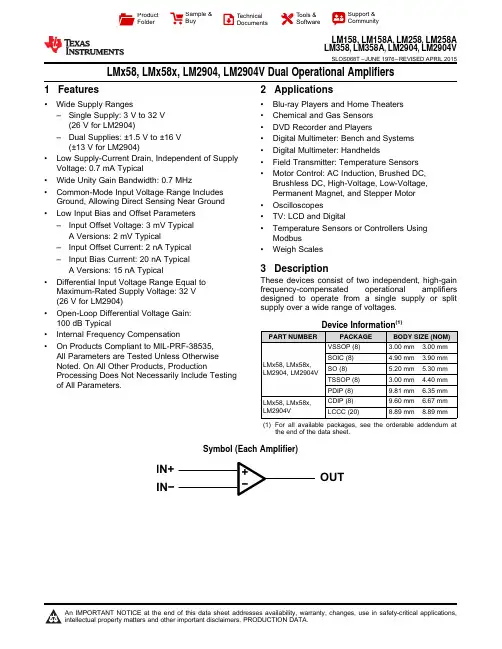
LM158, LM158A, LM258, LM258A LM358, LM358A, LM2904, LM2904V
SLOS068T – JUNE 1976 – REVISED APRIL 2015
Table of Contents
1 Features .................................................................. 1 2 Applications ........................................................... 1 3 Description ............................................................. 1 4 Revision History..................................................... 2 5 Pin Configuration and Functions ......................... 3 6 Specifications......................................................... 4
Brushless DC, High-Voltage, Low-Voltage, Permanent Magnet, and Stepper Motor • Oscilloscopes • TV: LCD and Digital • Temperature Sensors or Controllers Using Modbus • Weigh Scales
Device Information(1)
MAX13487EESA+
Half-Duplex RS-485-/RS-422-Compatible Transceiver with AutoDirection Control MAX13487E/MAX13488E
ABSOLUTE MAXIMUM RATINGS
(All voltages referenced to GND.) Supply Voltage VCC ...............................................................+6V SHDN, RE, DI..............................................................-0.3V to +6 A, B........................................................................... -8V to +13V Short-Circuit Duration (RO, A, B) to GND ..................Continuous Continuous Power Dissipation (TA = +70°C) 8-Pin SO (derate 5.9mW/°C above +70°C)..................471mW Operating Temperature Range ...........................-40°C to +85°C Junction Temperature ......................................................+150°C Storage Temperature Range .............................-65°C to +150°C Lead Temperature (soldering 10s) ..................................+300°C
MAX19705EVCMOD2中文资料
________________________________________________________________ Maxim Integrated Products
1
For pricing, delivery, and ordering information, please contact Maxim/Dallas Direct! at 1-888-629-4642, or visit Maxim’s website at .
Part Selection Table
PART MAX19705EVKIT MAX19706EVKIT MAX19707EVKIT MAX19708EVKIT SPEED (Msps) 7.5 22 45 11 DAC TRANSMIT FILTER Disabled Disabled Disabled Enabled
Evaluate: MAX19705–MAX19708
Ordering Information
PART MAX19705EVKIT TEMP RANGE IC PACKAGE I2C INTERFACE TYPE
0°C to 48 TQFN Not included +70°C 0°C to 48 TQFN MAX19705EVCMOD2 CMOD232 +70°C 0°C to 48 TQFN MAX19705EVCMODU CMODUSB +70°C 0°C to 48 TQFN MAX19706EVKIT Not included +70°C 0°C to 48 TQFN MAX19706EVCMOD2 CMOD232 +70°C 0°C to 48 TQFN MAX19706EVCMODU CMODUSB +70°C 0°C to 48 TQFN MAX19707EVKIT Not included +70°C 0°C to 48 TQFN MAX19707EVCMOD2 CMOD232 +70°C 0°C to 48 TQFN MAX19707EVCMODU CMODUSB +70°C 0°C to 48 TQFN MAX19708EVKIT Not included +70°C 0°C to 48 TQFN MAX19708EVCMOD2 CMOD232 +70°C 0°C to 48 TQFN MAX19708EVCMODU CMODUSB +70°C Note: The MAX19705–MAX19708 EV kit software is provided with the MAX19705EVKIT–MAX19708EVKIT; however, the CMOD232/CMODUSB board is required to interface the EV kit to the computer when using the included software.
马达驱动电路MX1508RX2产品手册_V1.1
传真:0755-26895685
4
SinotechMixic Electronics Co.,LTD
MX1508RX2
电特性参数表
(TA=25℃, VM =6.5V 除非另有规定)
参数
符号 条件
电源参数
VM 待机电流
IVMST
功 率 管 导通内阻
1 通道导通内阻
IO=±200mA VM1=6.5V TA=25℃ RON1 IO=±1000mA VM1=6.5V TA=25℃
该电路为功率器件,本身具备一定内阻,电路 的发热与负载电流、功率管导通内阻以及环境温度 密切相关。电路设计有芯片级温度检测电路,实时 监控芯片内部发热,当芯片内部温度超过设定值时, 产生功率管关断信号,关闭负载电流,避免因异常 使用导致的温度持续升高,进而造成塑料封装冒烟、 起火等严重安全事故。芯片内置的温度迟滞电路, 确保电路恢复到安全温度后,才允许重新对功率管 进行控制。
℃
TJ
150
℃
Tstg
-55~+150
℃
焊接温度
TLED
260℃,10 秒
注:(1)、VM 代表 VM1 和 VM2,1 通道代表 FORWARD 和 BACKWARD 通道,2 通道代表 RIGHT 和 LEFT 通道。
(2)、不同环境温度下的最大功耗计算公式为: PD=(150℃-TA)/θJA
解码频率
内置振荡频率
FOSC
允许发射频率的偏差
电特性曲线图
最小值 典型值 最大值 单位
465
uA
0.35 0.38
Ω 0.43 0.46
2.593 2.594
V 2.584 2.595
128
MAX4130EUK+T,MAX4130EUK+T,MAX4132ESA+,MAX4132EUA+,MAX4131ESA,MAX4131EBT+T, 规格书,Datasheet 资料
MAX4130–MAX4134________________________________________________________________Maxim Integrated Products1For pricing, delivery, and ordering information,please contact Maxim/Dallas Direct!at 1-888-629-4642, or visit Maxim’s website at .General DescriptionThe MAX4130–MAX4134 family of operational amplifiers combines 10MHz gain-bandwidth product and excellent DC accuracy with Rail-to-Rail ®operation at the inputs and outputs. These devices require only 900µA per amplifier, and operate from either a single supply (+2.7V to +6.5V) or dual supplies (±1.35V to ±3.25V) with a common-mode voltage range that extends 250mV beyond V EE and V CC . They are capable of driving 250Ωloads and are unity-gain stable. In addition, the MAX4131/ MAX4133 feature a shutdown mode in which the outputs are placed in a high-impedance state and the supply current is reduced to only 25µA per amplifier.With their rail-to-rail input common-mode range and output swing, the MAX4130–MAX4134 are ideal for low-voltage, single-supply operation. Although the minimum operating voltage is specified at 2.7V, the devices typically operate down to 1.8V. In addition, low offset voltage and high speed make them the ideal signal-conditioning stages for precision, low-voltage data-acquisition systems. The MAX4130 is offered in the space-saving 5-pin SOT23 package. The MAX4131 is offered in the ultra-small 6-bump, 1mm x 1.5mm chip-scale package (UCSP™).________________________ApplicationsBattery-Powered Instruments Portable Equipment Data-Acquisition Systems Signal ConditioningLow-Power, Low-Voltage ApplicationsFeatureso 6-Bump UCSP (MAX4131)o +2.7V to +6.5V Single-Supply Operationo Rail-to-Rail Input Common-Mode Voltage Rangeo Rail-to-Rail Output Voltage Swing o 10MHz Gain-Bandwidth Product o 900µA Quiescent Current per Amplifier o 25µA Shutdown Function (MAX4131/MAX4133)o 200µV Offset Voltageo No Phase Reversal for Overdriven Inputs o Drive 250ΩLoadso Stable with 160pF Capacitive Loads o Unity-Gain StableSingle/Dual/Quad, Wide-Bandwidth, Low-Power,Single-Supply, Rail-to-Rail I/O Op Amps19-1089; Rev 3; 3/03*Dice are specified at T A = +25°C. DC parameters only.Ordering Information continued at end of data sheet.Pin Configurations appear at end of data sheet.Rail-to-Rail is a registered trademark of Nippon Motorola, Ltd.UCSP is a trademark of Maxim Integrated Products, Inc.M A X 4130–M A X 4134Single/Dual/Quad, Wide-Bandwidth, Low-Power,Single-Supply Rail-to-Rail I/O Op Amps 2_______________________________________________________________________________________ABSOLUTE MAXIMUM RATINGSDC ELECTRICAL CHARACTERISTICS(V CC = +2.7V to +6.5V, V EE = 0V, V CM = 0V, V OUT = V CC /2, R L tied to V CC /2, SHDN ≥2V (or open), T A = +25°C , unless otherwise noted.)Stresses beyond those listed under “Absolute Maximum Ratings” may cause permanent damage to the device. These are stress ratings only, and functional operation of the device at these or any other conditions beyond those indicated in the operational sections of the specifications is not implied. Exposure to absolute maximum rating conditions for extended periods may affect device reliability.Supply Voltage (V CC - V EE )...................................................7.5V IN+, IN-, SHDN Voltage...................(V CC + 0.3V) to (V EE - 0.3V)Output Short-Circuit Duration (Note 1).......................Continuous(short to either supply)Continuous Power Dissipation (T A = +70°C)5-Pin SOT23 (derate 7.1mW/°C above +70°C)............571mW 6-Bump UCSP (derate 2.9mW/°C above +70°C).........308mW 8-Pin SO (derate 5.88mW/°C above +70°C)................471mW8-Pin µMAX (derate 4.10mW/°C above +70°C)...........330mW 14-Pin SO (derate 8.00mW/°C above +70°C)..............640mW Operating Temperature RangeMAX413_E__...................................................-40°C to +85°C Maximum Junction Temperature.....................................+150°C Storage Temperature Range.............................-65°C to +160°C Lead Temperature (soldering, 10s).................................+300°C Bump Reflow Temperature .........................................+235°CNote 1:Provided that the maximum package power-dissipation rating is not exceeded.MAX4130–MAX4134Single/Dual/Quad, Wide-Bandwidth, Low-Power,Single-Supply Rail-to-Rail I/O Op AmpsDC ELECTRICAL CHARACTERISTICS (continued)(V CC = +2.7V to +6.5V, V EE = 0V, V CM = 0V, V OUT = V CC /2, R L tied to V CC /2, SHDN ≥2V (or open), T A = +25°C , unless otherwise noted.)DC ELECTRICAL CHARACTERISTICS(V CC = +2.7V to +6.5V, V EE = 0V, V CM = 0V, V OUT = V CC /2, R L tied to V CC /2, SHDN ≥2V (or open), T A = -40°C to +85°C , unlessM A X 4130–M A X 4134Single/Dual/Quad, Wide-Bandwidth, Low-Power,Single-Supply Rail-to-Rail I/O Op Amps 4_______________________________________________________________________________________DC ELECTRICAL CHARACTERISTICS(V CC = +2.7V to +6.5V, V EE = 0V, V CM = 0V, V OUT = V CC /2, R L tied to V CC /2, SHDN ≥2V (or open), T A = -40°C to +85°C , unlessMAX4130–MAX4134Single/Dual/Quad, Wide-Bandwidth, Low-Power,Single-Supply Rail-to-Rail I/O Op Amps_______________________________________________________________________________________5DC ELECTRICAL CHARACTERISTICS (continued)(V CC = +2.7V to +6.5V, V EE = 0V, V CM = 0V, V OUT = V CC /2, R L tied to V CC /2, SHDN ≥2V (or open), T A = -40°C to +85°C , unless otherwise noted.) (Note 2)AC ELECTRICAL CHARACTERISTICSM A X 4130–M A X 4134Single/Dual/Quad, Wide-Bandwidth, Low-Power,Single-Supply, Rail-to-Rail I/O Op Amps 6_______________________________________________________________________________________60-401001k 10k 1M 10M100k 100M GAIN AND PHASE vs. FREQUENCY-20FREQUENCY (Hz)G A I N (d B )02040P H A S E (D E G R E E S )180144720-72-144-180-108-363610860-401001k 10k 1M 10M100k 100MGAIN AND PHASEvs. FREQUENCY (WITH C)-20FREQUENCY (Hz)G A I N (d B )2040P H A S E (D E G R E E S )180144720-72-144-180-108-36361080-100101001k100k1M10M10k 100MPOWER-SUPPLY REJECTIONvs. FREQUENCY-80FREQUENCY (Hz)P S R (d B )-60-40-2001051520253530454050-40-25-105203550658095SHUTDOWN SUPPLY CURRENTvs. TEMPERATURETEMPERATURE (°C)S U P P L Y C U R R E N T (µA )1000.100.011001k100k1M10M10k100MOUTPUT IMPEDANCE vs. FREQUENCYFREQUENCY (Hz)O U T P U T I M P E D A N C E (Ω)1101150800850900950105010001100-40-25-105203550658095SUPPLY CURRENT PER AMPLIFIERvs. TEMPERATURETEMPERATURE (°C)S U P P L Y C U R R E N T (µA )-10-505101520-40-25-105203550658095OUTPUT LEAKAGE CURRENTvs. TEMPERATURETEMPERATURE (°C)L E A K A G E C U R R E N T (µA )Typical Operating Characteristics(V CC = +5V, V EE = 0V, VCM = V CC / 2, T A = +25°C, unless otherwise noted.)-600123456INPUT BIAS CURRENT vs. COMMON-MODE VOLTAGECOMMON-MODE VOLTAGE (V)I N P U T B I A S C U R R E N T (n A )-50-40-30-20-10010203040-60-40-40-25-105203550658095INPUT BIAS CURRENTvs. TEMPERATURETEMPERATURE (°C)I N P U T B I A S C U R R E N T (n A )-200204060MAX4130–MAX4134Single/Dual/Quad, Wide-Bandwidth, Low-Power,Single-Supply, Rail-to-Rail I/O Op Amps_______________________________________________________________________________________712070750600110115OUTPUT VOLTAGE: EITHER SUPPLY (mV)G A I N (d B )30095859080100200500105100400LARGE-SIGNAL GAIN vs. OUTPUT VOLTAGE130-40-25-105203550658095LARGE-SIGNAL GAIN vs. TEMPERATURE90120TEMPERATURE (°C)G A I N (d B )11010085951251151051.21.31.51.41.61.71.81.9-40-25-105203550658095MINIMUM OPERATING VOLTAGEvs. TEMPERATUREM A X 4130/34-21TEMPERATURE (°C)M I N I M U M O P E R A T I N G V O L T A G E (V )Typical Operating Characteristics (continued)(V CC = +5V, V EE = 0V, V CM = V CC / 2, T A = +25°C, unless otherwise noted.)12080859095100105110115-40-25-105203550658095COMMON-MODE REJECTIONvs. TEMPERATURETEMPERATURE (°C)C O M M O N -M ODE R E J E C T I O N (d B )130700600120OUTPUT VOLTAGE: EITHER SUPPLY (mV)G A I N (dB )3001009080100200500110400LARGE-SIGNAL GAIN vs. OUTPUT VOLTAGE12060600110OUTPUT VOLTAGE: EITHER SUPPLY (mV)G A I N (d B )300908070100200500100400LARGE-SIGNAL GAIN vs. OUTPUT VOLTAGE12080-40-25-105203550658095LARGE-SIGNAL GAIN vs. TEMPERATURE90TEMPERATURE (°C)G A I N (d B )105859511511010012070750600110115OUTPUT VOLTAGE: EITHER SUPPLY (mV)G A I N (d B )30095859080100200500105100400LARGE-SIGNAL GAIN vs. OUTPUT VOLTAGE-3.00-2.25-0.75-1.5001.500.752.253.00-40-25-105203550658095INPUT OFFSET VOLTAGE vs. TEMPERATURETEMPERATURE (°C)V O L T A G E (m V )M A X 4130–M A X 4134Single/Dual/Quad, Wide-Bandwidth, Low-Power,Single-Supply, Rail-to-Rail I/O Op Amps 8_______________________________________________________________________________________1408010k 1k 100k 10M 1M CHANNEL SEPARATION vs. FREQUENCYFREQUENCY (Hz)C H A N N E L S E P A R A T I O N (d B )1009013011012010100k10kFREQUENCY (Hz)1001k 0.03000.0050.0100.0150.0200.025 TOTAL HARMONIC DISTORTION AND NOISE vs. FREQUENCYT H D A N D N O I S E (%)0.10.0014.04.44.25.04.84.6TOTAL HARMONIC DISTORTION AND NOISE vs. PEAK-TO-PEAK SIGNAL AMPLITUDEPEAK-TO-PEAK SIGNAL AMPLITUDE (V)T H D + N O I S E (%)0.01INTIME (200ns/div)V O L T A G E (50m V /d i v )OUTMAX4131SMALL-SIGNAL TRANSIENT RESPONSE (NONINVERTING)IN TIME (200ns/div)V O L T A G E (50m V /d i v )OUT MAX4131SMALL-SIGNAL TRANSIENT RESPONSE (INVERTING)A V = -1IN TIME (2µs/div)V O L T A G E (2V/d i v )OUT MAX4131LARGE-SIGNAL TRANSIENT RESPONSE (NONINVERTING)A V = +1INTIME (2µs/div)V O L T A G E (2V /d i v )OUTMAX4131LARGE-SIGNAL TRANSIENT RESPONSE (INVERTING)Typical Operating Characteristics (continued)(V CC = +5V, V EE = 0V, V CM = V CC / 2, T A = +25°C, unless otherwise noted.)1600-40-25-105203550658095MINIMUM OUTPUT VOLTAGEvs. TEMPERATURE20140120TEMPERATURE (°C)V O U T - V E E (m V )100806040050100150200250300-40-25-105203550658095MAXIMUM OUTPUT VOLTAGEvs. TEMPERATURETEMPERATURE (°C)V C C - V O U T (m V )MAX4130–MAX4134Single/Dual/Quad, Wide-Bandwidth, Low-Power,Single-Supply, Rail-to-Rail I/O Op Amps_______________________________________________________________________________________9Figure 1a. Reducing Offset Error Due to Bias Current (Noninverting)Figure 1b. Reducing Offset Error Due to Bias Current (Inverting)M A X 4130–M A X 4134Single/Dual/Quad, Wide-Bandwidth, Low-Power,Single-Supply, Rail-to-Rail I/O Op Amps 10______________________________________________________________________________________Applications InformationRail-to-Rail Input StageDevices in the MAX4130–MAX4134 family of high-speed amplifiers have rail-to-rail input and output stages designed for low-voltage, single-supply opera-tion. The input stage consists of separate NPN and PNP differential stages that combine to provide an input common-mode range that extends 0.2V beyond the supply rails. The PNP stage is active for input volt-ages close to the negative rail, and the NPN stage is active for input voltages near the positive rail. The input offset voltage is typically below 200µV. The switchover transition region, which occurs near V CC / 2, has been extended to minimize the slight degradation in com-mon-mode rejection ratio caused by the mismatch of the input pairs. Their low offset voltage, high band-width, and rail-to-rail common-mode range make these op amps excellent choices for precision, low-voltage data-acquisition systems.Since the input stage switches between the NPN and PNP pairs, the input bias current changes polarity as the input voltage passes through the transition region.Reduce the offset error caused by input bias currents flowing through external source impedances by match-ing the effective impedance seen by each input (Figures 1a, 1b). High source impedances, together with input capacitance, can create a parasitic pole that produces an underdamped signal response. Reducing the input impedance or placing a small (2pF to 10pF)capacitor across the feedback resistor improves response.The MAX4130–MAX4134s ’ inputs are protected from large differential input voltages by 1k Ωseries resistors and back-to-back triple diodes across the inputs (Figure 2). For differential input voltages less than 1.8V,input resistance is typically 500k Ω. For differential input voltages greater than 1.8V, input resistance is approxi-mately 2k Ω. The input bias current is given by the fol-lowing equation:Figure 2. Input Protection CircuitMAX4130–MAX4134Single/Dual/Quad, Wide-Bandwidth, Low-Power,Single-Supply, Rail-to-Rail I/O Op Amps______________________________________________________________________________________11Rail-to-Rail Output StageThe minimum output voltage is within millivolts of ground for single-supply operation where the load is referenced to ground (V EE ). Figure 3 shows the input voltage range and output voltage swing of a MAX4131connected as a voltage follower. With a +3V supply and the load tied to ground, the output swings from 0.00V to 2.90V. The maximum output voltage swing depends on the load, but will be within 150mV of a +3V supply, even with the maximum load (500Ωto ground).Driving a capacitive load can cause instability in most high-speed op amps, especially those with low quies-cent current. The MAX4130–MAX4134 have a high tol-erance for capacitive loads. They are stable with capacitive loads up to 160pF. Figure 4 gives the stable operating region for capacitive loads. Figures 5 and 6show the response with capacitive loads and the results of adding an isolation resistor in series with the output (Figure 7). The resistor improves the circuit ’s phase margin by isolating the load capacitor from the op amp ’s output.INTIME (1µs/div)V O L T A G E (1V /d i v )OUTV CC = 3V, R L = 10k Ω to V EEFigure 3. Rail-to-Rail Input/Output Voltage RangeFigure 4. Capacitive-Load StabilityINTIME (200ns/div)V O L T A G E (50m V /d i v )OUTV CC = 5V R L = 10k Ω C L = 130pFFigure 5. MAX4131 Small-Signal Transient Response with Capacitive Load Figure 6. MAX4131 Transient Response to Capacitive Load with Isolation ResistorINTIME (500ns/div)V O L T A G E (50m V /d i v )OUTV CC = 5V C L = 1000pF R S = 39ΩM A X 4130–M A X 4134Single/Dual/Quad, Wide-Bandwidth, Low-Power,Single-Supply, Rail-to-Rail I/O Op Amps 12______________________________________________________________________________________Power-Up and Shutdown ModeThe MAX4130–MAX4134 amplifiers typically settle with-in 1µs after power-up. Figures 9 and 10 show the out-put voltage and supply current on power-up, using the test circuit of Figure 8.The MAX4131 and MAX4133 have a shutdown option.When the shutdown pin (SHDN ) is pulled low, the sup-ply current drops below 25µA per amplifier and theamplifiers are disabled with the outputs in a high-impedance state. Pulling SHDN high or leaving it float-ing enables the amplifier. In the dual-amplifier MAX4133, the shutdown functions operate indepen-dently. Figures 11 and 12 show the output voltage and supply current responses of the MAX4131 to a shut-down pulse, using the test circuit of Figure 8.Figure 7. Capacitive-Load Driving CircuitFigure 8. Power-Up/Shutdown Test CircuitV CC TIME (5µs/div)V O L T A G E (1V /d i v )OUTFigure 9. Power-Up Output Voltage V CC (1V/div)TIME (5µs/div)I EE(500µA/div)Figure 10. Power-Up Supply CurrentMAX4130–MAX4134Single/Dual/Quad, Wide-Bandwidth, Low-Power,Single-Supply, Rail-to-Rail I/O Op Amps______________________________________________________________________________________13Power Supplies and LayoutThe MAX4130–MAX4134 operate from a single +2.7V to +6.5V power supply, or from dual supplies of ±1.35V to ±3.25V. For single-supply operation, bypass the power supply with a 0.1µF ceramic capacitor in parallel with at least 1µF. For dual supplies, bypass each sup-ply to ground.Good layout improves performance by decreasing the amount of stray capacitance at the op amp ’s inputs and outputs. Decrease stray capacitance by placing external components close to the op amp ’s pins, mini-mizing trace lengths and resistor leads.UCSP Applications InformationFor the latest application details on UCSP construction,dimensions, tape carrier information, PC board tech-niques, bump-pad layout, and the recommended reflow temperature profile, as well as the latest informa-tion on reliability testing results, go to Maxim ’s website at /ucsp and search for the Application Note: UCSP –A Wafer-Level Chip-Scale Package .TIME (1µs/div)OUTFigure 11. Shutdown Output Voltage TIME (1µs/div)Figure 12. Shutdown Enable/Disable Supply CurrentM A X 4130–M A X 4134Single/Dual/Quad, Wide-Bandwidth, Low-Power,Single-Supply, Rail-to-Rail I/O Op Amps 14________________________________________________________________________________________________________________________________________________Pin ConfigurationsMAX4130–MAX4134Single/Dual/Quad, Wide-Bandwidth, Low-Power,Single-Supply, Rail-to-Rail I/O Op Amps______________________________________________________________________________________15Chip InformationOrdering Information (continued)MAX4130 TRANSISTOR COUNT: 170MAX4131 TRANSISTOR COUNT: 170MAX4132 TRANSISTOR COUNT: 340MAX4134 TRANSISTOR COUNT: 680*Dice are specified at T A = +25°C, DC parameters only.Package Information(The package drawing(s) in this data sheet may not reflect the most current specifications. For the latest package outline information,go to /packages .)M A X 4130–M A X 4134Single/Dual/Quad, Wide-Bandwidth, Low-Power,Single-Supply, Rail-to-Rail I/O Op Amps 16______________________________________________________________________________________Package Information (continued)(The package drawing(s) in this data sheet may not reflect the most current specifications. For the latest package outline information,go to /packages .)MAX4130–MAX4134Single/Dual/Quad, Wide-Bandwidth, Low-Power,Single-Supply, Rail-to-Rail I/O Op Amps______________________________________________________________________________________17Package Information (continued)(The package drawing(s) in this data sheet may not reflect the most current specifications. For the latest package outline information,go to /packages .)Maxim cannot assume responsibility for use of any circuitry other than circuitry entirely embodied in a Maxim product. No circuit patent licenses are M A X 4130–M A X 4134Single/Dual/Quad, Wide-Bandwidth, Low-Power,Single-Supply, Rail-to-Rail I/O Op Amps implied. Maxim reserves the right to change the circuitry and specifications without notice at any time.18__________________Maxim Integrated Products, 120 San Gabriel Drive, Sunnyvale, CA 94086 (408) 737-7600©2003 Maxim Integrated ProductsPrinted USAis a registered trademark of Maxim Integrated Products.Package Information (continued)(The package drawing(s) in this data sheet may not reflect the most current specifications. For the latest package outline information,go to /packages .)。
- 1、下载文档前请自行甄别文档内容的完整性,平台不提供额外的编辑、内容补充、找答案等附加服务。
- 2、"仅部分预览"的文档,不可在线预览部分如存在完整性等问题,可反馈申请退款(可完整预览的文档不适用该条件!)。
- 3、如文档侵犯您的权益,请联系客服反馈,我们会尽快为您处理(人工客服工作时间:9:00-18:30)。
Maxim双通道偏置控制器MAX1385/6/11008
Maxim Integrated Products推出双通道RF LDMOS偏置控制器
MAX1385/MAX1386/MAX11008。这些高度集成的器件采用7mm×7mm封装,是业内最小的、集成
了蜂窝基站控制所需的所有模拟至数字(A/D)、数字至模拟(D/A)接口以及逻辑功能的LDMOS
偏置控制器。MAX1385/MAX1386/MAX11008非常适合为CDMA、GSM、EDGE和UMTS蜂窝基站中
功率放大器的功率晶体管提供偏置。
这些偏置控制器集成了PA信号链路中所需的所有功能,具有25μV (MAX1385/MAX1386)或
50μV (MAX11008)的自校准分辨率。MAX1385/MAX1386提供2个栅极驱动通道,每个通道包
含一个8位粗调DAC、10位精调DAC、以及增益为2 (MAX1385)或4 (MAX1386)的栅极驱动放
大器。这两个通道产生正栅极电压,以偏置LDMOS器件,分辨率高达18位。MAX11008的2
个栅极驱动通道均集成了12位DAC,以产生正栅极电压。
MAX1385/MAX1386/MAX11008包含一个7通道、12位ADC,其中3个通道用于温度测
量。此外,每款IC都带有两个高边电流检测放大器(32V,CMRR为90dB),其精度高达±0.5%,
12位时的线性度为1个最低有效位(LSB)。这些高边检流放大器具有2、10和25倍的可编程
增益,可在20mA至5A范围内监测LDMOS漏极电流。温度传感器的分辨率为0.25℃,精度高
达±1℃。
MAX11008包含4Kb片内非易失EEPROM,划分为256位×16位,用于存储查找表和寄
存器信息。MAX11008通过监测电流、电压和温度,决定是否调整DAC输出电压以维持偏置设
定。现有的其它方案则需外接EEPROM,并且还必须与外部处理器频繁通信。
3款偏置控制器均提供自校准模式,可减小整个时间、温度和电源电压范围内的误差。
此外,内部基准为ADC、DAC和温度传感器提供稳定的、低噪声、+2.5V基准电压,也允许ADC
和DAC灵活独立地使用外部基准。可通过20MHz、SPI兼容的4线串行接口或引脚可选的3.4MHz、
I2C兼容串行接口与IC进行通信。器件工作于+4.75V至+5.25V模拟电源以及+2.7V至+5.25V
数字电源。
MAX1385/MAX1386/MAX11008提供7mm×7mm、48引脚TQFN封装,工作于-40℃至+85℃
温度范围。芯片起价为$6.20 (1000片起,美国离岸价)。