数字设计:原理与实践第五版习题答案
数字设计(Digital Design)习题解答5

5–1E X E R C I S E S O L U T I O N S COMBINATIONAL LOGIC DESIGN PRINCIPLES55.4READY ′ is an expression, with ′ being a unary operator. Use a name like READY_L or /READY instead.5.8Both LOW -to-HIGH and HIGH -to-LOW transitions cause positive transitions on the outputs of three gates (every second gate), and negative transitions on the other three. Thus, the total delay in either case isSince and for a 74LS00 are identical, the same result is obtained using a single worst-case delay of 15 ns.5.12The smallest typical delay through one ’LS86 for any set of conditions is 10 ns. Use the rule of thumb, “mini-mum equals one-fourth to one-third of typical,” we estimate 3 ns as the minimum delay through one gate.Therefore, the minimum delay through the four gates is estimated at 12 ns.The above estimate is conservative, as it does not take into account the actual transitions in the conditions shown. For a LOW -to-HIGH input transition, the four gates have typical delays of 13, 10, 10, and 20 ns, a total of 53 ns, so the minimum is estimated at one-fourth of this or 13 ns. For a HIGH -to-LOW input transition, the four gates have typical delays of 20, 12, 12, and 13 ns, a total of 57 ns, so the minimum is estimated at 14 ns.5.15 A decoder with active-low outputs ought to be faster, considering that this decoder structure can be imple-mented directly with inverting gates (which are faster than noninverting) as shown in Figures 5–35 and 5–37.5.16The worst-case ’138 output will have a transition in the same direction as the worst-case ’139 output, so we uset pHL numbers for both, which is the worst combination. The delay through the ’139 is 38 ns, and from thet p 3t pLH(LS00)3t pHL(LS00)+=315⋅315⋅+=90 ns=t pLH t pHL5–2DIGITAL CIRCUITSactive-low enable input of the ’138 is 32 ns, for a total delay of 70 ns. Using “worst-case” numbers for the parts and ignoring the structure of the circuit, an overly pessimistic result of 79 ns is obtained.We can also work the problem with 74HCT parts. Worst-case delay through the ’139 is 43 ns, and from the active-low enable input of the ’138 is 42 ns, for a total delay of 85 ns. Ignoring the structure of the circuit, an overly pessimistic result of 88 ns is obtained.We can also work the problem with 74FCT parts. Worst-case delay through the ’139 is 9 ns, and from the active-low enable input of the ’138 is 8 ns, for a total delay of 17 ns. Ignoring the structure of the circuit, a slightly pessimistic result of 18 ns is obtained.Finally, we can work the problem with 74AHCT parts. Worst-case delay through the ’139 is 10.5 ns, and fromthe active-low enable input of the ’138 is 12 ns, for a total delay of 22.5 ns. Ignoring the structure of the circuit,a slightly pessimistic result of 23.5 ns is obtained. 5.195.21Both halves of the ’139 are enabled simultaneously when EN_L is asserted. Therefore, two three-state driverswill be enabled to drive SDATA at the same time. Perhaps the designer forgot to put an extra inverter on the signal going to 1G or 2G , which would ensure that exactly one source drives SDATA at all times.5.22The total delay is the sum of the decoding delay through the 74LS139, enabling delay of a 74LS151, and delaythrough a 74LS20: .5.25The worst-case delay is the sum of the delays through an ’LS280, select-to-output through an ’LS138, andthrough an ’LS86: .5.30The worst-case delay is the sum of four numbers:•In U1, the worst-case delay from any input to C4 (22 ns).•In U2, the worst-case delay from C0 to C4 (22 ns).•In U3, the worst-case delay from C0 to C4 (22 ns).•In U4, the worst-case delay from C0 to any sum output (24 ns).Thus, the total worst-case delay is 90 ns.5.35With the stated input combination, Y5_L is LOW and the other outputs are HIGH . We have the following cases:(a)Negating G2A_L or G2B_L causes Y5_L to go HIGH within 18 ns.(b)Negating G1 causes Y5_L to go HIGH within 26 ns.(c)Changing A or C causes Y5_L to go HIGH within 27 ns (the change propagates through 3 levels of logic internally), and causes Y4_L or Y1_L respectively to go LOW within 41 ns (2 levels).(d)Changing B causes Y5_L to go HIGH within 20 ns (2 levels), and causes Y7_L to go LOW within 39 ns (3levels). The delays in the ’LS138 are very strange—the worst-case for 3 levels is shorter than for 2 levels!383015++83ns =504130++121 ns =t pHLEXERCISE SOLUTIONS5–3 5.395.46The inputs are active low and the outputs are active high in this design.5–4DIGITAL CIRCUITS 5.47EXERCISE SOLUTIONS5–5 5.54An internal logic diagram for the multiplexer is shown below.5–6DIGITAL CIRCUITSA truth table and pin assignment for the mux are shown below.The mux can be built using a single PLD, a PAL20L8 or GAL20V8; the pin assignment shown above is based on the PLD. The corresponding ABEL program, MUX3BY5.ABL , is shown below. module Mux_3x5title '5-Bit, 3-Input Multiplexer J. Wakerly, Marquette University'MUX3BY5 device 'P20L8';" Input pinsI1D0, I1D1, I1D2 pin 23, 1, 2;I2D0, I2D1, I2D2 pin 3, 4, 5;I3D0, I3D1, I3D2 pin 6, 7, 8;I4D0, I4D1, I4D2 pin 9, 10, 11;I5D0, I5D1, I5D2 pin 18, 17, 16;S0, S1 pin 13, 14;" Output pinsY1, Y2, Y3, Y4, Y5 pin 22, 21, 20, 19, 15;" Set definitionsBUS0 = [I1D0,I2D0,I3D0,I4D0,I5D0];BUS1 = [I1D1,I2D1,I3D1,I4D1,I5D1];BUS2 = [I1D2,I2D2,I3D2,I4D2,I5D2];OUT = [Y1, Y2, Y3, Y4, Y5 ];" ConstantsSEL0 = ([S1,S0]==[0,0]);SEL1 = ([S1,S0]==[0,1]);SEL2 = ([S1,S0]==[1,0]);IDLE = ([S1,S0]==[1,1]);equationsOUT = SEL0 & BUS0 # SEL1 & BUS1 # SEL2 & BUS2 # IDLE & 0;end Mux_3x5InputsOutputsS1S01Y 2Y 3Y 4Y 5Y 001D02D03D04D05D0011D12D13D14D15D1101D22D23D24D25D21100000EXERCISE SOLUTIONS5–7 5.55This is the actual circuit of a MUX21H 2-input multiplexer cell in LSI Logic’s LCA 10000 series of CMOSgate arrays. When S is 0, the output equals A; when S is 1, the output equals B.5.605.67The ’08 has the same pinout as the ’00, but its outputs are the opposite polarity. The change in level at pin 3 ofU1 is equivalent to a change at pin 4 of U2 (the input of an X OR tree), which is equivalent in turn to a change at pin 6 of U2 (the parity-generator output). Thus, the circuit simply generated and checked odd parity instead of even.The change in level at pin 6 of U1 changed the active level of the ERROR signal.5.69This problem is answered in Section 5.9.3 of the text, which makes it a silly question.5–8DIGITAL CIRCUITS5.755.79The function has 65 inputs, and the worst 65-input function (a 65-input parity circuit) has terms in theminimal sum-of-products expression. Our answer can’t be any worse than this, but we can do better.The expression for has 3 product terms: The expression for is If we substitute our previous expression for c1 in the equation above and “multiply out,” we get a result with product terms. Let us assume that no further reduction is possible.Continuing in this way, we would find that the expression for has product terms and, in general, the expression for has product terms.Thus, the number of terms in a sum-of-products expression for is no more than , fewer if minimiza-tion is possible.2651–c 1c 1c 0x 0⋅c 0y 0⋅x 0y 0⋅++=c 2c 2c 1x 1⋅c 1y 1⋅x 1y 1⋅++=331++7=c 3771++15=c i 2i 1+1–c 322331–EXERCISE SOLUTIONS5–9 5.805–10DIGITAL CIRCUITS5.825.915.93The obvious solution is to use a 74FCT682, which has a maximum delay of 11 ns to its output. How-ever, there are faster parts in Table 5–3. In particular, the 74FCT151 has a delay of only 9 ns from any select input to Y or . To take advantage of this, we use a ’138 to decode the SLOT inputs statically and apply the resulting eight signals to the data inputs of the ’151. By applying GRANT[2–0] to the select inputs of the ’151, we obtain the MATCH_L output (as well as an active-high MATCH, if we need it) in only 9 ns!。
数电第五版第五章课后习题及答案演示精品PPT课件
【题5.15】已知CMOS边沿触发方式JK触发器各输入端 的电压波形如图P5.15所示,试画出Q,Q’端对应的电压 波形。
20
解:根据JK触发器逻辑功能的定义和边沿触发方式的动作特 点,画出的Q,Q’ 端电压波形如图A5.15。
21
【题5.18】设图P5.18中各触发器的初始状态皆为Q=0,试画 出在CLK信号连续作用下各触发器输出端的电压波形
10
解:根据SR触发器逻辑功能的定义及脉冲触发方式的动作特 点,即可画出图A5.8中Q和Q’的电压波形。
11
【题5.9】 若主从结构SR触发器的CLK,S,R, 各输入端电压波 形如图P5.9所示, =1,试画出Q,Q’ 端对应的电压波形。
12
解:根据SR触发器逻辑功能的定义及脉冲触发方式的动作特 点,即可画出Q,Q’的电压波形,如图A5.9所示。
学习要点: 1、不同电路结构触发器的动作 特点; 2、不同逻辑功能触发器的特性;
1
【题5.1】 画出图P5.1由与非门组成的SR锁存器输出端Q,Q’的 电压波形,输入端 , 的电压波形如图中所示。 解:见图A5.1.
No Image
2
3
【题5.4】图P5.4所示为一个防抖动输出的开关电路。当拨动 开关S时,由于开关触点接通瞬间发生振颤 , 和 的电压波 形如图中所示,试画出Q,Q’端对应的电压波形。
从高电平跳变成低电平以后电路的工作过程与上述过 程类似。这样就得到了图A5.20的 电压波形。
25
【题5.21】 在图P5.21所示的主从JK触发器电路中,CLK 和 A 的电压波形如图中所示,试画出 Q 端对应的电压波形。设触 发器的初始状态为 Q = 0.
26
写在最后
经常不断地学习,你就什么都知道。你知道得越多,你就越有力量 Study Constantly, And You Will Know Everything. The More
数电第五版_部分课后答案(清晰pdf康光华主编).txt

解:由图知该电路属于漏极开路门的线与输出
L E L4 E L1 L2 L3 E AB BC D
3.1.9 图题 3.1.9 表示三态门作总线传输的示意图,图中 n 个三态门的输出接到数据传 输总线,D1、D2、…、Dn 为数据输入端,CS1、CS2、…、CSn 为片选信号输入端。试问: (1)CS 信号如何进行控制,以便数据 D1、D2、…、Dn 通过该总线进行正常传输;(2)CS 信 号能否有两个或两个以上同时有效?如果 CS 出现两个或两个以上有效,可能发生什么情 况?(3)如果所有 CS 信号均无效,总线处在什么状态?
2 / 31
(3) A ABC ACD (C D) E A CD E
A ABC ACD (C D) E A(1 BC ) ACD (C D) E A(1 CD) ACD CDE A CD CDE A CD(1 E ) CDE A CD E
解: L ACD BCD ABCD ACD( B B) ( A A) BCD ABCD
ABCD ABCD ABCD ABCD ABCD m13 m9 m10 m 2 m15
(2) L A( B C )
L A( B C ) A ( B C ) A( BC BC ) BC ABC ABC BC ( A A) ABC A( B C ) ABC ABC ABC ABC ABC AB (C C ) AC ( B B ) ABC ABC ABC ABC ABC ABC ABC ABC ABC ABC ABC ABC m 7 m 5 m1 m 4 m 6
数字设计原理与实践答案整理

1.3ASIC Application-Specific Integrated CircuitCAD Computer-Aided DesignCD Compact DiscCO Central OfficeCPLD Complex Programmable Logic DeviceDIP Dual In-line PinDVD Digital Versatile DiscFPGA Field-Programmable Gate ArrayHDL Hardware Description LanguageIC Integrated CircuitIP Internet ProtocolLSI Large-Scale IntegrationMCM Multichip ModuleMSI Medium-Scale IntegrationNRE Nonrecurring EngineeringPBX Private Branch ExchangePCB Printed-Circuit BoardPLD Programmable Logic DevicePWB Printed-Wiring BoardSMT Surface-Mount TechnologySSI Small-Scale IntegrationVHDL VHSIC Hardware Description LanguageVLSI Very Large-Scale Integration1.4ABEL Advanced Boolean Equation LanguageCMOS Complementary Metal-Oxide SemiconductorJPEG Joint Photographic Experts GroupMPEG Moving Picture Experts GroupOK 据说是Oll Korrect(All Correct)的缩写。
数字设计原理与实践第7章作业答案

第七章作业答案7.4 画出图7-4中所示的S-R锁存器的输出波形,其输入波形如图X7-2所示。
假设输入和输出信号的上升和下降时间为0,或非门的传播延迟是10ns(图中每个时间分段是10ns)7.5 用图X7-4中的输入波形重作练习题7-5。
结果可能难以置信,但是这个特性在转移时间比传输时间延迟短的真实器件中确实会发生。
7.6 图7-34表示出了怎样用带有使能端的D触发器和组合逻辑来构造T触发器。
请表示出如何用带有使能端的T触发器和组合逻辑来构造D触发器。
解:对于带使能端的T触发器,EN=0时状态不变,EN=1时状态变化,列出D触发器的状态转换表可得:D Q Q* EN0 0 0 00 1 0 11 0 1 11 1 1 07.7 请指出如何使用带有使能端的T触发器和组合逻辑来构造J-K触发器。
解:列出J-K触发器的状态转换表可得:Q J K Q* EN0 0 00 00 0 1 0 00 1 0 1 10 1 1 1 11 0 0 1 01 0 1 0 11 1 0 1 01 1 1 0 1JK ENQ 00 01 11 101EN=J·Q’+K·Q7.18 分析图x7—18中的时钟同步状态机,写出激励方程、激励/转移表,以及状态/输出表(状态Q2Q1QO=000—111使用状态名A—H)。
解:激励方程:)21()01()21()01(2'⋅'⊕⊕='+⊕⊕=QQQQQQQQD21QD=1 11 1XYQ1Q2 00 01 1011 00 00 10 00 10 01 00 10 00 10 10 00 11 00 10 11 00 11 0010EN1EN2XYQ1Q2 00 01 10 11 00 00,1 10,1 00,0 10,0 01 01,0 11,0 01,0 11,0 10 10,1 01,1 10,0 00,0 11 11,000,011,001,0Q1*Q2*,ZXY S 00 01 10 11 A A,1 C,1 A,0 C,0 B B,0 D,0 B,0 D,0 C C,1 B,1 C,0 A,0 D D,0A,0D,0B,0S*,Z10Q D =7.20分析图X7—20中的时钟同步状态机。
数字设计原理与实践课后答案
若是 7 状态或者 8 状态呢?
解:3 位二进制编码有 8 种形式。
对于 5 状态,这是一个 8 中取 5 的排列:N=8x7x6x5x4= 6720
对于 7 状态,这是一个 8 中取 7 的排列:N=8x7x6x5x4x3x2= 40320 对于 8 状态,种类数量与 7 状态时相同。 2.34 若每个编码字中至少要含有一个 0,对于表 2-12 的交通灯控制 器,有多少种不同的 3 位二进制编码方式? 解:在此条件下,只有 7 种可用的 3 位二进制码,从中选取 6 个进行 排列,方式数量为:N=7x6x5x4x3x2=5040 2.35 列出图 2-5 的机械编码盘中可能会产生不正确位置的所有“坏” 边界。 解:001/010、011/100、101/110、111/000 2.36 作为 n 的函数,在使用 n 位二进制编码的机械编码盘中有多少 个“坏”边界? 解:有一半的边界为坏边界:2n-1。
13 画出 NOR3 对应的电路图。 解:3 输入端或非门结构应为:上部 3 个 P 管串联,下部 3 个 N 管并 联,结构如图所示。
3.15 画出 OR2 所对应的电路图。 解:在 NOR2 电路的输出端后面级联一个 INV。
(h) AB3D16=43837
(i) 71568=3694
(j) 15C.3816=348.21875
2.6 完成下面的数制转换。
(a) 125= 1 111 1012 (b) 3489= 66418 (c) 209= 11 010 0012
(d) 9714= 227628
(e) 132= 10 000 1002 (f) 23851= 5D2B16
(g) 727= 104025
(h) 57190=DF6616 (i) 1435=26338
数字设计原理与实践第四章答案

=W X Y Z Z+W X X Y Z
+W W X Y Z +W X Y Y Z
0
习题4.6(b)
F = A B +A B C D+A B D E+A B C E+A B C E
F X Y Z = X,Y,Z (1, 2, 4, 7) FD = X,Y,Z (0,3,5,6) X,Y,Z (1,2, 4, 7) =F
所以是自对偶的
习题4.47
(e)F’(A,B,…,Z)=FD(A’,B’,…,Z’) FD(A,B,…,Z)=F’(A’,B’,…,Z’) P135 当为1的变量数大于3个时,
00 01
11
10 0
0 0
0 0
0
习题4.24
(X+Y)(X'+Z)=XX'+XZ+X'Y+YZ = XZ+X'Y+YZ (由T11) =XZ+X'Y 证毕 习题4.25
N输入与门可以由N-1个2输入的与来实现。 对于N输入与非门是不可以由N-1个2输入的 与非门来实现的。可举反例来证明。
F=A B A B+A B
习题4.36
A
B
F
0 0 1 1
0 1 0 1
1 0 0 1
F=A
B A B+A B
习题4.39
两输入的与非门可以构成完全集; 由题可知,2 输入的与门,或门,反相器可 以构成完全集,所以只要证明 2 输入的与门, 或门,反相器可以由与非门来表示, AB=((AB)')'=((AB)'·1)' A+B=((A+B)')'=(A'·B')' =((A·A)'·(B·B)')' A'=(A·A)'
数电第五版答案阎石第一三章(完整资料).doc

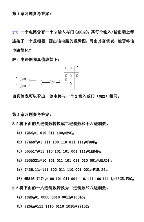
【最新整理,下载后即可编辑】第一章1.1 二进制到十六进制、十进制(1)(10010111)2=(97)16=(151)10 (2)(1101101)2=(6D)16=(109)10(3)(0.01011111)2=(0.5F)16=(0.37109375)10 (4)(11.001)2=(3.2)16=(3.125)10 1.2 十进制到二进制、十六进制(1)(17)10=(10001)2=(11)16(2)(127)10=(1111111)2=(7F)16(3) (0.39) 10 (0.0110 0011 1101 0111 0000 101 0)2 (0.63 D70 A )161.8 用公式化简逻辑函数(1)Y=A+B(2)Y ABC A B C 解:Y BC A B C C A B C (1 A+A=1)(4)Y ABCD ABD ACD 解:Y AD(BC B C ) AD(B C C) AD(5)Y=0(4) (25.7) 10 (11001.101 1 0011)2 (19.B3)16(3)Y=1(7)Y=A+CD(6)Y AC(CD AB) BC(B AD CE) 解:Y BC(B AD CE) BC(B AD) CE ABCD(C E ) ABCDE(8)Y A (B C)(A B C)(A B C) 解:Y A (B C)(A B C)(A B C) A (ABC BC)(A B C) A BC( A B C) A ABC BC A BC(9)Y BC AD AD(10)Y AC AD AEF BDE BDE1.9 (a) Y ABC BC(b)(c) Y1 AB AC D,Y2 AB AC D ACD ACD (d) Y1 AB AC BC,Y2 ABC ABC ABC ABC 1.10 求下列函数的反函数并化简为最简与或式Y ABC ABC(1) (2)Y A C DY AC BC(3)Y (A B)(A C)AC BC 解:Y ( A B)(A C)AC BC [(A B)(A C) AC] BC(4)Y A B C ( AB AC BC AC)(B C) B C【最新整理,下载后即可编辑】(5)Y AD AC BCD C 解:Y (A D)(A C)(B C D)C AC(A D)(B C D) ACD(B C D) ABCD1.11 将函数化简为最小项之和的形式(6)Y 0(1)Y ABC AC BC 解:Y ABC AC BC ABC A(B B )C ( A A)BC ABC ABC ABC ABC ABC ABC ABC ABC ABC(2)Y ABCD ABCD ABCD ABCD ABCD ABCD (3)Y A B CD解:Y A(BC D BCD BCD BCD BC D BCD BCD BCD) B( ACD ACD ACD ACD AC D ACD ACD ACD) (AB AB AB AB)CD ABC D ABCD ABCD ABCD ABC D ABCD ABCD ABCD ABC D ABCD ABCD ABCD ABCD (13)(4)Y ABCD ABCD ABCD ABC D ABCD ABCD ABCD ABCD (5)Y LM N LMN LMN LMN L M N LMN1.12 将下列各函数式化为最大项之积的形式(1)Y (A B C )( A B C)( A B C )(2)Y (A B C)( A B C)( A B C)(3)Y M 0 M 3 M 4 M 6 M 7(4) Y M 0 M 4 M 6 M 9 M12 M13(5)Y M 0 M 3 M 51.13 用卡诺图化简法将下列函数化为最简与或形式:(1)Y A D(3)Y 1(2)Y AB AC BC CD(4)Y AB AC BC(5)Y B C DY C D AB(7)(9)Y B D AD BC ACD (8)Y ( A, B, C, D) m (0,1,2,3,4,6,8,9,10,11,14)Y AB AC(6)Y AB AC BCY C(10)Y ( A, B, C) (m1,m4 , m7 )Y B CD AD 【最新整理,下载后即可编辑】Y ABC ABC ABC1.14 化简下列逻辑函数 (1)Y A B C D (3)Y AB D AC (5)Y AB DE CE BDE AD ACDE1.20 将下列函数化为最简与或式 (1)Y ACD BCD AD (3)Y A B C (5)Y 1 第三章3.1 解:由图可写出 Y1、Y2 的逻辑表达式:Y1 ABC ( A B C) AB AC BC ABC ABC ABC ABCY2 AB AC BC真值表:(2)Y CD ACD (4)Y BC BD(2)Y B AD AC (4)Y A B D (6)Y CD B D AC3.2 解: , comp 1、Z 0 时,Y1 A,Y2 A2,Y3 A2 A3 A2 A3,Y4 A2 A3 A4comp 0、Z 0 时,Y1 A1,Y2 A2,Y3 A3,Y4 A真值表:3.3 解:【最新整理,下载后即可编辑】3.4 解:采用正逻辑,低电平=0,高电平=1。
- 1、下载文档前请自行甄别文档内容的完整性,平台不提供额外的编辑、内容补充、找答案等附加服务。
- 2、"仅部分预览"的文档,不可在线预览部分如存在完整性等问题,可反馈申请退款(可完整预览的文档不适用该条件!)。
- 3、如文档侵犯您的权益,请联系客服反馈,我们会尽快为您处理(人工客服工作时间:9:00-18:30)。
数字设计:原理与实践第五版习题答案
第一章:数字系统基础
1. 哪些数学符号代表布尔逻辑运算?分别代表哪些逻辑操作?
布尔逻辑运算包括与(AND)、或(OR)、非(NOT)、
异或(XOR)等运算。
它们的对应数学符号表示如下:•与(AND):$\\cdot$ 或 $\\land$
•或(OR):+或 $\\lor$
•非(NOT):$\\overline{A}$ 或eee
•异或(XOR):$\\oplus$
2. 简述数字系统的信号表示和信号处理单元。
数字系统的信号表示使用离散量来表示连续或离散的信号,其中离散量指代具有离散数值的量。
信号处理单元是指对输入信号进行处理和操作的硬件模块,用于实现特定的功能或执行特定的任务。
3. 什么是布尔函数?它可以用哪些方法表示?
布尔函数是指以布尔逻辑运算为基础,将一个或多个布尔变量映射为单一布尔值的函数。
布尔函数可以用真值表、逻辑表达式和逻辑图等方法表示。
4. 简述数字系统的设计方法。
数字系统的设计方法包括以下几个步骤:
1.确定问题的需求和约束条件。
2.将问题抽象为逻辑功能的实现。
3.设计逻辑电路并进行仿真验证。
4.实现电路设计并进行实验验证。
5.优化电路设计并进行性能评估。
6.完成设计文档和报告。
第二章:组合逻辑电路设计
1. 什么是组合逻辑电路?简述其基本特征。
组合逻辑电路是指将组合逻辑块进行组合形成的电路,其
输出仅依赖于当前的输入。
它的基本特征包括:
•输入输出之间无时序关系。
•只有组合逻辑块,没有存储元件。
•输出仅取决于当前输入。
2. 简述逻辑门的功能和特点。
逻辑门是实现布尔逻辑运算的基本构件,其功能和特点如下:
•与门(AND):多个输入信号全部为高时,输出高;
否则输出低。
•或门(OR):多个输入信号有一个为高时,输出高;
否则输出低。
•非门(NOT):输入信号为高时,输出低;否则输出高。
•异或门(XOR):多个输入信号中奇数个为高时,输出高;否则输出低。
3. 什么是选择器和解码器?
选择器是一种组合逻辑电路,根据选择信号将一组输入信号中的某一个作为输出。
解码器是一种多输入和多输出的组合逻辑电路,通过对输入进行译码,选通一个或多个输出。
4. 什么是复用器和译码器?
复用器是一种多输入和单输出的组合逻辑电路,通过一个选择输入信号选择其中一个输入作为输出。
译码器是一种多输入和多输出的电路,将某个编码形式的输入转换为相应的输出形式。
第三章:时序逻辑电路设计
1. 什么是时序逻辑电路?简述其基本特征。
时序逻辑电路是指组合逻辑电路和存储元件结合形成的电路,其输出不仅依赖于当前的输入,还可能依赖于历史输入。
其基本特征包括:
•有存储元件(如触发器)用于存储数据。
•输出除了和当前输入有关外,还可能和之前的输入有关。
•可实现存储和状态功能。
2. 简述触发器的功能和工作原理。
触发器是一种存储元件,用于存储一位或多位数据。
它的功能是存储输入数据,并根据时钟信号的上升沿或下降沿触发进行存储和更新。
触发器的工作原理:
•D触发器:根据时钟信号,输入信号直接传递到输出。
•JK触发器:通过时钟信号和输入信号进行置位和复位。
•T触发器:通过时钟信号和输入信号进行翻转。
3. 什么是计数器?简述其基本类型。
计数器是一种时序逻辑电路,用于计数和存储数据。
常见的计数器有以下几种类型:
•二进制计数器:将计数值表示为二进制数,按特定规律递增或递减。
•同步计数器:所有触发器的时钟信号相同。
•异步计数器:触发器的时钟信号不同,每个触发器依赖于前一个触发器的输出。
4. 简述状态机的功能和基本类型。
状态机是一种时序逻辑电路,用于描述和控制系统的状态转换。
状态机的功能包括:
•存储当前的状态。
•根据输入和当前状态确定下一个状态。
•根据当前状态和输入生成输出。
常见的状态机类型有以下几种:
•Moore状态机:输出仅与当前状态有关。
•Mealy状态机:输出不仅与当前状态有关,还与输
入有关。
•有限状态自动机:仅有有限个状态。
以上是《数字设计:原理与实践》第五版部分习题的答案,希望对您的学习有所帮助!。