Minimum Density Interconnection Trees
PCB工程资料中常见的英文缩写汇总
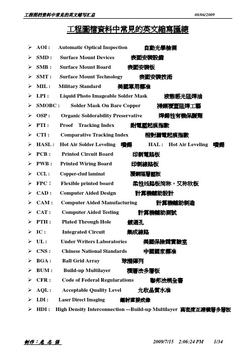
工程圖檔資料中常見的英文縮寫匯總¾AOI : Automatic Optical Inspection 自動光學檢測¾SMD : Surface Mount Devices 表面安裝設備¾SMB : Surface Mount Board 表面安裝板¾SMT : Surface Mount Technology 表面安裝技術¾MIL : Military Standard 美國軍用標准¾LPI : Liquid Photo Imageable Solder Mask 液態感光阻焊油¾SMOBC : Solder Mask On Bare Copper 裸銅覆蓋阻焊工藝¾OSP : Organic Solderability Preservative 焊錫性有機保護劑¾PTI : Proof Tracking Index 耐電壓起痕指數¾CTI : Comparative Tracking Index 相對漏電起痕指數¾HASL : Hot Air Solder Leveling 噴錫HAL : Hot Air Leveling 噴錫¾PCB : Printed Circuit Board 印制電路板¾PWB : Printed Wiring Board 印制線路板¾CCL : Copper-clud laminat 覆銅箔層壓板¾FPC: Flexible printed board 柔性线路板简称,又称软板¾CAD : Computer Aided Design 計算機輔助設計¾CAM : Computer Aided Manufacturing 計算機輔助制造¾CAT : Computer Aided Testing 計算機輔助測試¾PTH : Plated Through Hole 鍍通孔¾IC : Integrated Circuit 集成線路¾UL : Under Writers Laboratories 美國保險商實驗室¾CNS : Chinese National Standards 中國國家標准¾BGA : Ball Grid Array 球柵陣列¾BUM : Build-up Multilayer 積層法多層板¾CFR : Code of Federal Regularations 聯邦法規全書¾AQL : Acceptable Quality Level 允收品質水准¾LDI : Laser Direct Imaging 鐳射直接成像¾HDI : High Density Interconnection –-Build-up Multilayer 高密度互連積層多層板1.依照標准(in according with related standards):IPC : The Institute for International and Packaging Electronic Circuit美國電路互連與安裝學NEMA : National Electronic Manufacturing Association 國家電子制造協會/美國電氣制造協會2.基本材料 ( base material):natural color 自然色 external copper weight 外層銅厚copper clad覆銅箔prepreg 預浸材料(指半固化膠片)Tg rating 玻璃化溫度laminate 基板cross-section切片cutout 切口Metal core 金屬芯type of board 板類 (single sided 單面 double sided 雙面 multilayer 多層)epoxy glass fiber 環氧玻璃纖維flammability rating/class 防火等級dielectric material 介質材料temperature 溫度Resin Content 膠含量Glass Transition Temperature (由”玻璃态”转化为”橡皮态”简称为TG!)base copper (基銅)3.偏差及公差(deviation & tolerance) :registration 對位(重合度) dimension (長/寬/高)尺寸大小 radius &diameter半徑/直徑hole size/aperture孔徑 width 寬度length 長度 depth深度height 高度thickness 厚度spacing間距axis軸coordinate坐標parameter參數copper foil 銅箔board outline/contour 板輪廓圖 edge to edge 邊到邊heat sink plane 散熱層stack up 疊層 $ 疊放 finish(ed) thickness 完成厚度trace = track = line = pattern = conductor =rail = circuit 線路top layer 上層& bottom layer 下層 layer to layer registration 層與層對位inter layer & external layer 內層&外層clearance 空隙、間空、間隔 & gap 間隙guide hole = pilot hole導引孔tangency 切線、相接觸&diagonal對角線、對頂線signal plane 信號層voltage plane電源層 ground plane 接地層C/S=component side 元件面 S/S=solder side 焊接面Primary side 主層secondary side 輔層 supporting plane 支撐面Film 底片/菲林master film 主稿片artwork 底稿片master drawing布設總圖4. 工藝(process):surface finishing = surface treatment = finish 表面處理hard gold 重金Entek / Flux 防氧化Immersion Ag 化银gold plating 鍍金immersion gold 沉金flash gold 閃金tin / lead plating 鍍鉛錫electroless gold (plating)(無電)鍍金nickel /gold plating 鍍鎳金HASL : Hot Air Solder Leveling 噴錫 HAL : Hot Air Leveling 噴錫NPTH : Not Plated Through Hole 非鍍通孔(非電鍍孔)Flat package type平裝型SMOBC : Solder Mask On Bare Copper 裸銅覆阻焊工藝 plug through hole 塞孔Void 空洞slot 開槽 / 槽孔 tented vias掩孔 / 導通孔 annular ring 孔環mounting hole安裝孔 tooling hole 管位孔(定位孔)wet solder mask濕膜dry film /dry solder mask干膜preflux & postflux 預塗助焊劑&後塗助焊劑carbon ink 碳油silkscreen legend 絲印字符 non-conductive 非導電的Permanent 耐久的Solder resist阻焊劑 & solder mask 阻焊油(膜)Flow soldering 流焊Reflow soldering 再流焊 Wave soldering 波焊Dip soldering 浸焊Drag soldering 曳焊Float soldering 浮焊withdrawal lacquer = peelable solder mask 藍膠2. 25mm window around fiducial without solder resistOverall diameter of solder resist free area = 6.0mm5. 標識(marking ):vender’s identification (賣主身份) = manufacture’s identification (制造商名)= company name (公司名稱)date code 生產周期 UL logo (denotation) UL標識trademark 商標type designation 型號標志 revision letter 版本字母dustbin symbol 垃圾箱標志stamp 蓋印、壓印short /open test 短/斷路測試 liable to read易於辯认6.彎曲與扭曲 (bow and twist or twist and warp ):not exceed 不超過7. 外形(profiling):mechnical outline 外形圖 countersink 鑽孔route bit 鑼鑽頭score 劃痕、刻痕、劃線 score line分割線 slot 開槽 / 槽孔& cutouts 切口panelization detail 拼板圖cosmetic =appearance外觀keepout area 保留區域breakaway rails 沖破導線array size 拼板尺寸punch 沖床drill 鑽孔route 鑼板V-cut 切割、分割8. 清潔度(clealiness):Finished circuit board shall be free of dirt ,oil ,ionic contaminates or other foreign matter which could affect solderability circuit performance ,lift or appearance 。
PCB名语解释

4. Solder mask: 阻焊剂
5. Peelable solder mask: 蓝胶
6. Carbon Ink:碳油
7. Dry film :干膜
8. RCC : Resin Coated Copper (不含玻璃布)
第三篇:
有关工序
1. PTH: (Plated through hole) 电镀孔 PTH
Breaking Tab
V-Cut
T h e r m a l / C l e a r a n c e
9. Thermal:
(heat shield)热隔离盘 (大面积导电图形上,元件周
围被蚀刻掉的部分)
作用:它使在焊接时因截面过分散热而产生虚焊的可
能性减少。
10. Clearance:
无铜空间(通常指铜皮上为孔开的无铜区域)
BGA/CSP
CSP--- Chip Scale package
说明:
它们都是一种封装技术。 在PCB上都表现为一 VIA孔联了一个焊接 PAD。
BGA Pad Line
Via Hole
要求:
一般BGA区域VIA孔要求 塞孔
5. Fiducial mark :
作用:
Fiducial mark
正常范围指: 沉银与防氧化 3-5mil, 沉金 4-6mil, 喷锡
1.3 Multi孔应以通孔的最小钻嘴为准(而非VOP孔与盲埋孔);
2. MI中关于某些制作的标准化表述
2.1 电镀板边, MI确定某几层需要连通后, 表述如下例(浅色字内 容视具体要求而变):
“保证1、3、4、6层电镀后互相连接,其余层保证铜到板边 10mil”
4.1 MI上的所有参数(如线宽、间等等), 如无特别说明, 均指 生产后的完成值
hdi标准

hdi标准
HDI即高密度互连板(High Density Interconnection,HDI),指线路密集、高多层、钻孔小于0.15mm的电路板。
HDI标准涉及多个方面,包括设备、人员和生产管控。
在设备方面,HDI需要全新的设备,前期投入资金十分庞大。
例如,CO激光成孔机平均每部50~60万美元,水平镀铜生产线PTH/CuPlating平均250~300万美元,细线曝光的激光直接成像设备超100万美元,细线与阻焊曝光的设备超100万美元,精密压合机同样百万美元以上。
此外,为放置各种先进设备,还必须配有无尘车间。
在人员方面,HDI生产需要配备多名专业的工程师。
具体包括激光钻孔工程师、HDI压合工程师、HDI全流程工艺工程师、线路工程师、阻焊工程师、高级工程研发人员等。
可见其生产操作的技术门槛是较高的。
在生产管控方面,HDI板厂需要拥有完整的生产体系,全工序不外发,严控产品质量。
以上信息仅供参考,如需了解更多信息,建议咨询专业人士。
浅谈HDI简介及工艺流程

OLYMPIC (HESHAN) PCB CO.,LTD.
鹤山市世运电路科技有限公司
二 HDI之主要特征
• 短线 • 布线长度短。 • 薄层 • 介电层厚度薄。 • 潜孔 • 导通孔的传输长度短。 • 备注:以上三个特征共同的特性就是提高
•
(5)固化后绝缘层厚度要Байду номын сангаас匀;
Olympic (Heshan) PCB Co., LTD. OLYMPIC (HESHAN) PCB CO.,LTD.
鹤山市世运电路科技有限公司
Olympic (Heshan) PCB Co., LTD. OLYMPIC (HESHAN) PCB CO.,LTD.
鹤山市世运电路科技有限公司 鹤山世运电路科技有限公司
Olympic (Heshan) PCB Co., LTD. OLYMPIC (HESHAN) PCB CO.,LTD.
鹤山市世运电路科技有限公司
一、背景: 随着生产技术的不断演进,电子产品无不 趋向轻薄短小的方向发展,今天各种包括移 动电话、数码摄像机等微型手提式电子产品 都是高密度互连(High Density Interconnect,HDI)技术发展下的应用市 场。高密度互连是目前最新的线路板制程技 术,通过微孔的形成,线路板层与层之间能 互相连接,而这种高密度互连制程,再配合 增层法技术的采用,从而使线路板能实现朝 薄和小的方向发展。
其板外逐次增加线路层,并以非机械钻孔式之盲孔做
为增层间的互连,而在部分层次间连通的盲孔
(Blind Hole)与埋孔(Buried Hole),可省下通孔在 板面上的占用空间,有限的外层面积尽量用以布线和
IPC标准中英名称对照

Sided Flex Circuits 单面和双面挠性电路组装导则 IPC-FC-234 Composite Metallic Materials Specification for Printed Wiring Boards 印制线路板复合金属材料规范 IPC-MB-380 Guidelines for Molded Interconnection Devices 模压互连器件导则 IPC-M-107 Standards for Printed Board Materials Manual 印制板材料标准手册 IPC-MI-660 Incoming Inspection of Raw Materials Manual 原材料接收检验手册 IPC-4101A Specifications for Base Materials for Rigid and Multilayer Printed Boards 刚性及多层印制板用基材规范 IPC-4121 Guidelines for Selecting Core Construction for Multilayer Printed Wiring Board Applications 多层印制板用芯板结构选择导则 IPC-4562 Metal Foil for Printed Wiring Applications 印制线路用金属箔 IPC-CF-148A Resin Coated Metal for Printed Boards 印制板用涂树脂金属箔 IPC-CF-152B Composite Metallic Materials Specification for Printed Wiring Boards 印制线路板复合金属材料规范 IPC-TR-482 New Developments in Thin Copper Foils 薄铜箔的新发展 IPC-TR-484 Results of IPC Copper Foil Ductility Round Robin Study IPC铜箔延展性联合研究结果 IPC-TR-485 Results of Copper Foil Rupture Strength Test Round Robin Study 铜箔断裂强度试验联合研究结果
基板与镀孔厚度的关系_概述及解释说明

基板与镀孔厚度的关系概述及解释说明1. 引言1.1 概述本文旨在探讨基板与镀孔厚度之间的关系,并对其进行解释和说明。
随着电子器件的不断发展和微小化趋势,要求更高性能的印制电路板(PCB)已成为现代电子产品的核心组成部分。
而镀孔作为实现各种功能性器件连接和布线的重要步骤,其厚度对PCB及其所应用的电子器件性能至关重要。
1.2 文章结构本文主要包括以下几个方面内容:首先,我们将介绍基板材料及其性质对镀孔厚度产生影响的背景知识。
然后,我们会详细阐述镀孔过程中各种因素对厚度形成的影响情况。
接下来,我们将介绍实验设计与方法,以便更好地研究基板与镀孔厚度之间的关系。
在结果与讨论部分,我们将探究不同基板材料和镀孔工艺参数对厚度调控能力以及其对器件性能的影响进行分析。
最后,我们将总结研究结果,并展望未来进一步深入研究该领域的可能性。
1.3 目的本文的主要目标是系统地调查、分析和阐述基板与镀孔厚度之间的关系。
通过对该关系进行全面的解释和说明,我们将为研究人员、工程师以及相关领域的决策者提供更深入的理解,并为今后完善、优化电子器件设计和生产过程提供有价值的参考。
2. 基板与镀孔厚度的关系:2.1 基板材料与性质:基板是印刷电路板(PCB)中一种重要的材料。
不同的基板材料具有不同的性质,如导电性、热传导性和机械强度等。
这些性质会直接影响到镀孔过程中形成的镀层厚度。
常见的基板材料包括玻璃纤维增强环氧树脂(FR-4)、聚酰亚胺(PI)和聚四氟乙烯(PTFE)等。
FR-4是最常用的基板材料,其导热系数较低,而PI和PTFE 具有更高的导热性能。
因此,不同基板材料在镀孔过程中会产生不同的温度分布,从而对镀层厚度产生影响。
2.2 镀孔过程及影响因素:在PCB制造过程中,为了提供良好的电连接,需要进行钻孔并通过镀铜来形成导电通路。
然而,镀孔过程受到许多因素的影响,包括电流密度、浸泡时间、酸碱度和温度等。
电流密度是一个重要参数,它决定了镀孔过程中铜离子的迁移速率。
全球高密度互连印制电路板市场格局研究
全球高密度互连印制电路板市场格局研究杨宏强【摘要】高密度互连板(HDI PCB)是一种重要的、技术含量较高的印制电路板.基于HDI的相关概念、发展历程和应用,详细分析了全球HDI PCB的主要制造地(日本、中国台湾、韩国、中国大陆、其他等)及其主要制造商的现状,总结了全球16家HDI PCB制造商的产品布局.【期刊名称】《印制电路信息》【年(卷),期】2018(026)009【总页数】8页(P6-13)【关键词】高密度互连印制电路板;发展历程;主要制造商;市场格局【作者】杨宏强【作者单位】【正文语种】中文【中图分类】TN411 高密度互连印制电路板概述1.1 相关概念高密度互连印制电路板英文缩写为HDI PCB~HDI是High Density Interconnect的缩写,它是二十世纪八十年代以来电子产品(或部件)追求轻、薄、短、小,采用高密度化设计的一种印制板。
相对常规印制板,它的单位面积布线密度很高,主要表现特征为细线路、微盲孔、薄介电层等。
高密度印制板在发展过程中有多种称谓,如Micro-via Multi-layer PCB(微盲孔多层板)、Build-up Multi-layer PCB(BUM,积层多层板或者增层多层板)等,现在业界统称为HDI PCB。
现在,业界对HDI PCB的限定条件有:最小的线宽/间距在75 µm/75 µm及以下;最小的导通孔孔径在150 µm及以下;含有盲孔或盲埋孔、最小焊盘在400 µm及以下;焊盘密度大于20cm2等。
目前,多层FPC、高多层板、刚—挠性结合板等也在局部甚至全部区域内采用HDI工艺来制造,但业界习惯上将其仍归为原来的类别,本文也遵从此习惯。
但是考虑到目前大多数中高端的刚-挠性结合板(本文特指刚性板区域采用HDI技术,下同)是由HDI公司制造的(其技术难点是刚性板区域的制作(见图1),故从技术角度,本文将其纳入HDI范围(但各公司刚—挠性结合板的营收额仍归为刚—挠性结合板类别)。
数据结构(最小生成树)
(Minimum Cost Spanning Tree)
问题:
假设要在 n 个城市之间建立通信联 络网,则连通 n 个城市只需要修建 n-1 条线路,如何在最节省经费的前提下 建立这个通信网?
问题分析:
▪ 由于在每两个城市之间都可以建立一
条通信线路,n个城市之间最多可能设 置n(n-1)/2条线路,而每条线路都要
付出一定的经济代价,因此,如何从
中选择n-1条线路使总的耗费最少成为
问题的关键。
问题等价:
▪ 用连通网来表示n个城市以及n个城
市之间可能设置的通信线路,其中 网中的顶点表示城市,边表示两城 市之间的线路,赋于边的权值表示 相应的经济代价。 ▪ 建立总花费最少的通信网问题就转 换为求连通网的最小生成树的问题。
设置一个辅助数组closedge,来记录 从顶点集U到V-U具有最小代价的边。
A
6
5
B5
1
D
5
C
36
4
2
E6
F
Prim算法
U
V-U
B C D E F TE
{A}
Hale Waihona Puke {B,C,D,E, AB AC AD ~ ~ AC
F}
6 1 5∞∞ 1
{A,C}
CB {B,D,E,F}
5
AD CE CF CF 564 4
返回
克鲁斯卡尔算法的基本思想:
考虑问题的出发点: 为使生成树上边的权值之 和达到最小,则应使生成树中每一条边的权值 尽可能地小。
具体做法: 先构造一个只含 n 个顶点的子图 SG,然后从权值最小的边开始,若它的添加 不使SG 中产生回路,则在 SG 上加上这条边, 如此重复,直至加上 n-1 条边为止。 一句话,“不构成环的情况下,每次选取最小 边”
最小树最短路以及动态规划思想.
3
v0
10
v1
21
11
5
19
n -3
v5 33 14 6
v2 6
v4
18
v3
100
10 0
5
6
19
1211
5 6
0 6
6 0
18
14
1291
11
18 14
0 33
303
Hu Junfeng
27
mst[5]={{0,1,10}, {1,2,5}, {1,3,6}, {1,5,11} , {3,4,18}}
18
14
1291
11
18 14
0 33
303
26
mst[5]={{0,1,10}, {1,2,5}, {1,3,6}, {3,4,18}, {1,5,11} } mst[5]={{0,1,10}, {1,2,5}, {1,3,6}, {3,4,18}, {1,5,11} }
v0
10
v1
21
11
5
v5
19 33 14 6
v2
6
v4
18
v3
Hu Junfeng
0 10 19 21
10 0 5 6 11
5 0 6
6 6 0 18 14
19 21
11
18 14
0 33
33 0
24
① n=6,只有顶点v0在最小生成树中。 mst[5]={{0,1,10}, {0,2,∞}, {0,3,∞}, {0,4,19}, {0,5,21} }
图 第二讲
Genesis软件对HDI印制板精细线路补偿设计的研究
Genesis软件对HDI印制板精细线路补偿设计的研究作者:梁素霞来源:《科技创新与应用》2018年第27期摘要:文章通过使用Genesis2000软件对HDI线路板的精细线路做特殊补偿,同时对其板边SYMBOL进行优化设计,从而达到对精细线路蚀刻均匀性的管控及提高良率的目的。
通过Genesis2000软件对精细线路特殊补偿设计后,采用最佳的蚀刻参数,制作出的精细线路品质良好,符合IPC品质要求,而且批次合格率大大提高。
关键词:Genesis2000;HDI;精细线路板;补偿设计中图分类号:TN41 文献标志码:A 文章编号:2095-2945(2018)27-0091-03Abstract: By using Genesis2000 software to make special compensation for the flexible circuit of HDI circuit board and to optimize the design of SYMBOL on the edge of the board, the purpose of controlling the etching uniformity of fine circuit and improving the yield is achieved. After special compensation design of flexible circuit by Genesis2000 software, the fine circuit made by adopting the best etching parameters has good quality and meets the quality requirements of IPC, and the batch pass rate is greatly improved.Keywords: Genesis2000; HDI; flexible printed circuit board (FPC); compensation design1 概述HDI板(High Density Interconnection)一般是指高端印制线路板,因为目前我们的电子设备都是正在快速地往高精密度及高信赖度等方向发展,所以高端HDI印制板的线宽和线距也随之设计得越来越精细,现在一般常见的线宽线距都是3mil,最小的已经达到2mil了。
- 1、下载文档前请自行甄别文档内容的完整性,平台不提供额外的编辑、内容补充、找答案等附加服务。
- 2、"仅部分预览"的文档,不可在线预览部分如存在完整性等问题,可反馈申请退款(可完整预览的文档不适用该条件!)。
- 3、如文档侵犯您的权益,请联系客服反馈,我们会尽快为您处理(人工客服工作时间:9:00-18:30)。
CS Dept., University of California at Los Angeles, Los Angeles, CA 90024-1596 y CS Dept., University of Virginia, Charlottesville, VA 22903-2442 z EECS Dept., Northwestern University, IL 60208-3118
Minimum Density Interconnection Trees C. J. Alpert,J. Cong,A. B. Kahng,G. Robins,M. Sarrafzadeh Technical Report No. CS-92-35 October 1, 1992
Minimum Density Interconnection Trees
1
determine the impact of a given interconnection topology on the chip area. For a detailed treatment of integrated circuit routing methodologies, the reader is referred to 14].
1 Introduction
In this paper, we address a new problem formulation for spanning and Steiner tree constructions in the Manhattan plane. Our objective is to minimize the density of such interconnection trees, where density re ects a concept that is closely related to the stabbing number studied in computational geometry 8]. The motivation for our work lies in the area minimization requirement that is implicit in the global routing phase of VLSI layout; global routing entails building (spanning or Steiner) interconnection trees over given signal nets which correspond to point sets in the Manhattan plane. Traditionally, minimization of total edgelength in the tree is used to approximately capture the goal of minimizing the total area of the chip, since wires have a xed width and must be routed at a xed separation from each other. However, the structure of integrated circuit routing resources allows us to more precisely
De nition: The density of an interconnection tree is the maximum number of tree edges properly
2
intersected by any horizontal or vertical line in the plane (Figure 2).1
(a)
(b)
(c)
Figure 2: (a) Example of a signal net, along with (b) an interconnection tree with density 3, and (c) a minimum density tree with density 2. In our work, we will address the following:
De nition: For a given net N , the minimum density of N is the minimum density achievable by an
interconnection tree T (N ), and a minimum density interconnection tree is any T (N ) that achieves this density.
Partial support for this work was provided by a Department of Defense Graduate Fellowship; by NSF MIP-9110511; by NSF MIP-9110696, NSF Young Investigator Award MIP-9257982, ARO DAAK-70-92-K-0001, and ARO DAAL-0392-G-0050; and by an IBM Graduate Fellowship.
(a)
(b)
Figure 1: A four-point example for which the tree on the left has density 3, but the tree on the right has density 2. We say that a signal net N is a set of n points, or terminals, p1; p2; : : : ; pn 2 N in the Manhattan plane. If necessary, we may distinguish p1 as a source terminal, with the remaining members of N being sink terminals. An interconnection tree of a net N , denoted T (N ), is a tree which spans N . The cost of a routing tree T is the sum of the costs of its edges, where the cost of an edge is the Manhattan distance between its endpoints. Without loss of generality, we assume that the terminal coordinates are scaled so that the entire signal net lies within the unit square.
1.1 Problem Formulaห้องสมุดไป่ตู้ion
Consider the example of Figure 1, which depicts four terminals of a signal net. The interconnection tree in Figure 1(a) forces at least three wires to cross the dashed line, meaning that the vertical dimension of the chip must be large enough accomodate at least this many so-called routing tracks 14]. In contrast, the routing of Figure 1(b) only forces the vertical chip dimension to grow by one routing track (although the horizontal dimension grows by one track, as shown by the horizontal dashed line). In general, the most e ective use of chip area will be attained if the chip dimensions are roughly equal; this suggests a balancing of the horizontal and vertical routing requirements induced by the interconnection tree. With the example of Figure 1 in mind, we develop the Minimum Density Interconnection Tree problem as follows.
Minimum Density Interconnection Tree (MDIT) Problem: Given a net N , nd a minimum
Abstract
We discuss a new minimum density objective for spanning and Steiner tree constructions in the plane. This formulation is motivated particularly by the need for balanced usage of routing resources to achieve minimum-area VLSI layouts. We present two e cient heuristics for constructing low-density spanning trees, and prove that their outputs are within small constants of optimal with respect to both tree weight and density. Our proof techniques suggest a non-uniform lower bound schema, which may be used to establish the quality of the heuristic solution for any given instance. More interesting is the fact that the minimum density objective can be transparently combined with a number of previous interconnection objectives, without a ecting the solution quality with respect to these previous metrics. As examples, we show how sets of competing measures (e.g., cost, density, radius; or cost, density, skew) can be simultaneously optimized. Extensive simulation results suggest that applications to VLSI global routing are promising.