1019, 规格书,Datasheet 资料
CDBK0530;中文规格书,Datasheet资料
+125OCTSTG
SymbolTypParameterConditionsMinMaxUnit
Forward voltageIF = 500mAIF = 100mA
VFV
0.47
0.36
Reverse currentCapacitance between terminalsVR = 20V
f = 1 MHz, and 0 VDC reverse voltageI
R
CT
uApF100
100
CDBK0530QW-A1106OMaximum Rating (at TA=25C unless otherwise noted)
OElectrical Characteristics (at TA=25C unless otherwise noted)
Page 1
TypIO
VRVRMAverage forward rectified currentReverse voltagePeak reverse voltageForward current,surge peakSymbolParameterConditionsMinMaxUnitVVA0.5
2030
Tj
Storage temperatureJunction temperatureOC
+125
-40IFSM
8.3 ms single half sine-wave superimposed
on rate load (JEDEC method)2A
REV:A
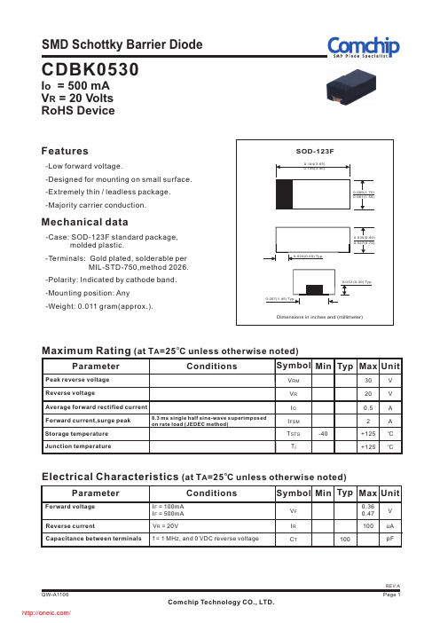
0.144(3.65)0.136(3.45)
0.024(0.60) Typ.0.069(1.75)0.061(1.55)
0.035(0.90)0.027(0.70)
Dimensions in inches and (millimeter)
SOD-123F
0.012 (0.30) Typ.0.057(1.45) Typ.
Comchip Technology CO., LTD.
SMD Schottky Barrier DiodeFeatures -Low forward voltage. -Designed for mounting on small surface. -Extremely thin / leadless package. -Majority carrier conduction.Mechanical data -Case: SOD-123F standard package, molded plastic.
BB181,115;BB181,135;BB181,335;中文规格书,Datasheet资料
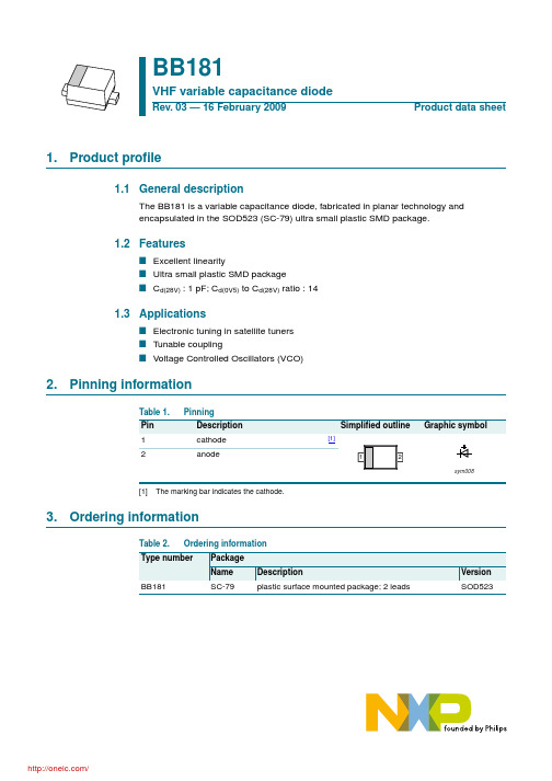
1.Product profile1.1General descriptionThe BB181 is a variable capacitance diode, fabricated in planar technology and encapsulated in the SOD523 (SC-79) ultra small plastic SMD package.1.2FeaturesI Excellent linearityI Ultra small plastic SMD packageI C d(28V): 1pF; C d(0V5) to C d(28V) ratio : 141.3ApplicationsI Electronic tuning in satellite tuners I Tunable couplingI Voltage Controlled Oscillators (VCO)2.Pinning information[1]The marking bar indicates the cathode.3.Ordering informationBB181VHF variable capacitance diodeRev. 03 — 16 February 2009Product data sheetTable 1.PinningPin Description Simplified outline Graphic symbol1cathode [1]2anode21sym008Table 2.Ordering informationType numberPackage NameDescriptionVersion BB181SC-79plastic surface mounted package; 2 leadsSOD5234.MarkingTable 3.Marking codesType number Marking codeBB181N5.Limiting valuesTable 4.Limiting valuesIn accordance with the Absolute Maximum Rating System (IEC 60134).Symbol Parameter Conditions Min Max UnitV R reverse voltage-30VI F forward current-20mAT stg storage temperature−55+150°CT j junction temperature−55+150°C 6.CharacteristicsTable 5.CharacteristicsT j = 25°C unless otherwise specified.Symbol Parameter Conditions Min Typ Max Unit I R reverse current see Figure2V R=30V--10nAV R=30V; T j=85°C--200nAr s diode series resistance f=470MHz at C d=9pF--3ΩC d diode capacitance f=1MHz; see Figure1 andFigure3V R=0.5V8-17pFV R=28V0.7- 1.055pFC d(0V5)/C d(28V)diode capacitance ratio (0.5V to 28V) f = 1 MHz12-16f = 1 MHz; T j = 25°C.Fig 1.Diode capacitance as a function of reverse voltage; typical valuesmbe87210515C d (pF)0V R (V)10−1102101T j = 0°C to 85°C.Fig 2.Reverse current as a function of junction temperature; maximum valuesFig 3.Temperature coefficient of diode capacitance as a function of reverse voltage; typical valuesmlc81610210103I R (nA)1T j (°C)010080406020mlc81511010−310−410−510−1102V R (V)TC d (K −1)7.Package outline8.Abbreviations9.Revision historyFig 4.Package outline SOD523 (SC-79)REFERENCESOUTLINE VERSION EUROPEAN PROJECTIONISSUE DATE IECJEDECJEITA SOD523SC-7902-12-1306-03-16Plastic surface-mounted package; 2 leadsSOD52300.5 1 mmscaleD 12H EEb pAcv M AAUNITb pc D E v mmA H E DIMENSIONS (mm are the original dimensions)Note1. The marking bar indicates the cathode.(1)0.340.260.170.110.10.850.751.251.150.650.581.651.55Table 6.AbbreviationsAcronym DescriptionSMD Surface Mounted Device VHFVery High FrequencyTable 7.Revision historyDocument IDRelease date Data sheet status Change notice Supersedes BB181_320090216Product data sheet-BB181_N_2Modifications:•The format of this data sheet has been redesigned to comply with the new presentation and information standard of NXP semiconductorsBB181_N_220080102Product data sheet -BB181_1BB181_119981126Product specification--10.Legal information10.1Data sheet status[1]Please consult the most recently issued document before initiating or completing a design.[2]The term ‘short data sheet’ is explained in section “Definitions”.[3]The product status of device(s)described in this document may have changed since this document was published and may differ in case of multiple devices.The latest product status information is available on the Internet at URL .10.2DefinitionsDraft —The document is a draft version only. The content is still under internal review and subject to formal approval, which may result in modifications or additions. NXP Semiconductors does not give any representations or warranties as to the accuracy or completeness ofinformation included herein and shall have no liability for the consequences of use of such information.Short data sheet —A short data sheet is an extract from a full data sheet with the same product type number(s)and title.A short data sheet is intended for quick reference only and should not be relied upon to contain detailed and full information. For detailed and full information see the relevant full data sheet, which is available on request via the local NXP Semiconductors sales office. In case of any inconsistency or conflict with the short data sheet, the full data sheet shall prevail.10.3DisclaimersGeneral —Information in this document is believed to be accurate andreliable.However,NXP Semiconductors does not give any representations or warranties,expressed or implied,as to the accuracy or completeness of such information and shall have no liability for the consequences of use of such information.Right to make changes —NXP Semiconductors reserves the right to make changes to information published in this document, including withoutlimitation specifications and product descriptions, at any time and without notice.This document supersedes and replaces all information supplied prior to the publication hereof.Suitability for use —NXP Semiconductors products are not designed,authorized or warranted to be suitable for use in medical, military, aircraft,space or life support equipment, nor in applications where failure ormalfunction of an NXP Semiconductors product can reasonably be expected to result in personal injury, death or severe property or environmentaldamage. NXP Semiconductors accepts no liability for inclusion and/or use of NXP Semiconductors products in such equipment or applications and therefore such inclusion and/or use is at the customer’s own risk.Applications —Applications that are described herein for any of these products are for illustrative purposes only. NXP Semiconductors makes no representation or warranty that such applications will be suitable for the specified use without further testing or modification.Limiting values —Stress above one or more limiting values (as defined in the Absolute Maximum Ratings System of IEC 60134)may cause permanent damage to the device.Limiting values are stress ratings only and operation of the device at these or any other conditions above those given in theCharacteristics sections of this document is not implied. Exposure to limiting values for extended periods may affect device reliability.Terms and conditions of sale —NXP Semiconductors products are sold subject to the general terms and conditions of commercial sale,as published at /profile/terms , including those pertaining to warranty,intellectual property rights infringement and limitation of liability, unless explicitly otherwise agreed to in writing by NXP Semiconductors. In case of any inconsistency or conflict between information in this document and such terms and conditions, the latter will prevail.No offer to sell or license —Nothing in this document may be interpreted or construed as an offer to sell products that is open for acceptance or the grant,conveyance or implication of any license under any copyrights,patents or other industrial or intellectual property rights.10.4TrademarksNotice:All referenced brands,product names,service names and trademarks are the property of their respective owners.11.Contact informationFor more information, please visit:For sales office addresses, please send an email to:salesaddresses@Document status [1][2]Product status [3]DefinitionObjective [short] data sheet Development This document contains data from the objective specification for product development.Preliminary [short] data sheet Qualification This document contains data from the preliminary specification.Product [short] data sheetProductionThis document contains the product specification.12.Contents1Product profile. . . . . . . . . . . . . . . . . . . . . . . . . . 11.1General description. . . . . . . . . . . . . . . . . . . . . . 11.2Features . . . . . . . . . . . . . . . . . . . . . . . . . . . . . . 11.3Applications . . . . . . . . . . . . . . . . . . . . . . . . . . . 12Pinning information. . . . . . . . . . . . . . . . . . . . . . 13Ordering information. . . . . . . . . . . . . . . . . . . . . 14Marking. . . . . . . . . . . . . . . . . . . . . . . . . . . . . . . . 25Limiting values. . . . . . . . . . . . . . . . . . . . . . . . . . 26Characteristics. . . . . . . . . . . . . . . . . . . . . . . . . . 27Package outline . . . . . . . . . . . . . . . . . . . . . . . . . 48Abbreviations. . . . . . . . . . . . . . . . . . . . . . . . . . . 49Revision history. . . . . . . . . . . . . . . . . . . . . . . . . 410Legal information. . . . . . . . . . . . . . . . . . . . . . . . 510.1Data sheet status . . . . . . . . . . . . . . . . . . . . . . . 510.2Definitions. . . . . . . . . . . . . . . . . . . . . . . . . . . . . 510.3Disclaimers. . . . . . . . . . . . . . . . . . . . . . . . . . . . 510.4T rademarks. . . . . . . . . . . . . . . . . . . . . . . . . . . . 511Contact information. . . . . . . . . . . . . . . . . . . . . . 512Contents. . . . . . . . . . . . . . . . . . . . . . . . . . . . . . . 6Please be aware that important notices concerning this document and the product(s)described herein, have been included in section ‘Legal information’.© NXP B.V.2009.All rights reserved.For more information, please visit: For sales office addresses, please send an email to: salesaddresses@Date of release: 16 February 2009分销商库存信息:NXPBB181,115BB181,135BB181,335。
CSD25201W15;中文规格书,Datasheet资料
Device
Package
Media Qty
CSD25201W15
1.5-mm × 1.5-mm Wafer Level Package
7-Inch Reel
3000
Ship
Tape and Reel
DESCRIPTION
The device has been designed to deliver the lowest on resistance and gate charge in the smallest outline possible with excellent thermal characteristics in an ultra low profile. Low on resistance coupled with the small footprint and low profile make the device ideal for battery operated space constrained applications.
0.0001 0.0001
0.001
Duty Cycle = t1/t2
P
t1 t2
Typical Rq JA = 227° C/W (min Cu) TJ = P ´ Zq JA ´ Rq JA
0.01
0.1
1
10
100
1k
tp - Pulse Duration - s
G012
Figure 1. Transient Thermal Impedance
VGS Gate to Source Voltage
Continuous Drain Current(1)(2)
ID
astm1019-18标准

astm1019-18标准
ASTM1019-18是美国材料与试验协会(ASTM International)
制定的标准,该标准规定了用于评估和指导玛钦加工的一般性要求。
ASTM1019-18标准涵盖了以下方面:
1. 材料的选择和处理:标准对玛钦加工所使用的材料的特性、质量和处理要求进行了规定,以确保加工过程中的材料符合所需的性能和质量标准。
2. 设备和工具:标准规定了适用于玛钦加工的设备和工具的要求,包括机床、刀具、模具等,以确保加工过程中的设备和工具能够满足加工要求和保持其性能。
3. 加工技术:标准涵盖了玛钦加工的各个方面,包括切削力和切削速度的控制、刀具选择和使用、加工过程中的冷却和润滑等,以确保加工过程中的质量和效率。
4. 检验和测试:标准规定了对玛钦加工后产品的检验和测试方法,以评估产品的质量和性能,包括尺寸、表面粗糙度、力学性能等。
ASTM1019-18标准的应用范围广泛,适用于各种材料的玛钦
加工,包括金属、塑料、复合材料等。
这个标准的目的是帮助制造商和用户确保他们的产品能够满足规定的性能和质量要求,并确保加工过程的可靠性和一致性。
MBR0530;中文规格书,Datasheet资料

Thermal Characteristics
Symbol
Parameter
RθJA RθJL
Thermal Resistance, Junction to Ambient * Thermal Resistance, Junction to Lead
* 1 inch square pad size on FR-4 board.
¥
Saving our world, 1mW/W/kW at a time™ SignalWise¥ SmartMax¥ SMART START¥ Solutions for Your Success¥ SPM® STEALTH¥ SuperFET® SuperSOT¥-3 SuperSOT¥-6 SuperSOT¥-8 SupreMOS® SyncFET¥ Sync-Lock™
ANTI-COUNTERFEITING POLICY
Fairchild Semiconductor Corporation's Anti-Counterfeiting Policy. Fairchild's Anti-Counterfeiting Policy is also stated on our external website, , under Sales Support.
March 2012
SOD123 Color Band Denotes Cathode
Mark: B3
Absolute Maximum Ratings *
Values are at TA=25°C unless otherwise noted.
Symbol
Parameter
Value
Unit
VRRM Maximum Repetitive Reverse Voltage
MC14513BCPG;中文规格书,Datasheet资料

−
0.05
0
0.05
−
0.05
Vin = 0 or VDD
“1” Level
VOH
5.0
4.1
10
9.1
− −
4.1 9.1
5.0 10
15
14.1
−
14.1
15
−
4.1
−
Vdc
−
9.1
−
−
14.1
−
Output Voltage — RBO Output “0” Level
Vin = VDD or 0
IOHmax
25
mA
Current (Source) per Output
Maximum Continuous Output Power POHmax
50
mW
(Source) per Output (Note 2)
Stresses exceeding Maximum Ratings may damage the device. Maximum Ratings are stress ratings only. Functional operation above the Recommended Operating Conditions is not implied. Extended exposure to stresses above the Recommended Operating Conditions may affect device reliability. 1. Temperature Derating: Plastic “P and D/DW”
Vin = 0 or VDD
“1” Level