DS5003FPM-16中文资料
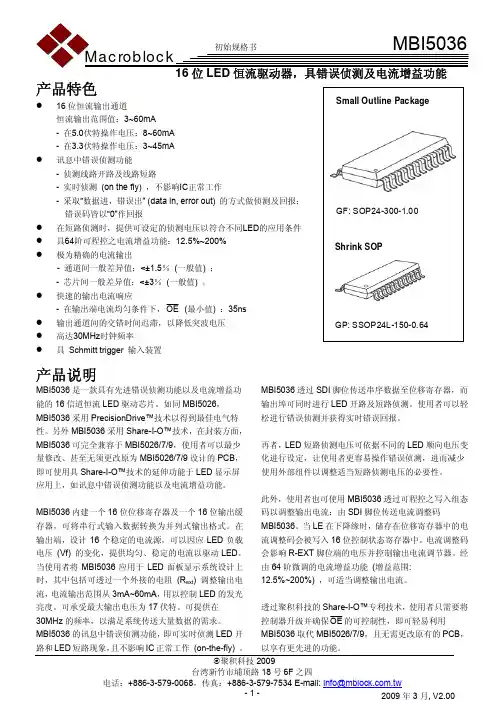
MBI5036中文资料
产品特色z 16位恒流输出通道恒流输出范围值:3~60mA- 在5.0伏特操作电压:8~60mA- 在3.3伏特操作电压:3~45mAz讯息中错误侦测功能- 侦测线路开路及线路短路- 实时侦测(on the fly) ,不影响IC正常工作- 采取“数据进,错误出” (data in, error out) 的方式做侦测及回报;错误码皆以“0”作回报z在短路侦测时,提供可设定的侦测电压以符合不同LED的应用条件z具64阶可程控之电流增益功能:12.5%~200%z极为精确的电流输出- 通道间一般差异值:<±1.5%(一般值) ;- 芯片间一般差异值:<±3%(一般值) 。
z快速的输出电流响应- 在输出端电流均匀条件下,OE(最小值) :35nsz输出通道间的交错时间迟滞,以降低突波电压z高达30MHz时钟频率z具 Schmitt trigger 输入装置产品说明MBI5036是一款具有先进错误侦测功能以及电流增益功能的16信道恒流LED驱动芯片。
如同MBI5026,MBI5036采用PrecisionDrive™技术以得到最佳电气特性。
另外MBI5036采用Share-I-O™技术,在封装方面,MBI5036可完全兼容于MBI5026/7/9,使用者可以最少量修改、甚至无须更改原为MBI5026/7/9设计的PCB,即可使用具Share-I-O™技术的延伸功能于LED显示屏应用上,如讯息中错误侦测功能以及电流增益功能。
MBI5036内建一个16位位移寄存器及一个16位输出缓存器,可将串行式输入数据转换为并列式输出格式。
在输出端,设计16个稳定的电流源,可以因应LED负载电压 (Vf) 的变化,提供均匀、稳定的电流以驱动LED。
当使用者将MBI5036应用于LED面板显示系统设计上时,其中包括可透过一个外接的电阻 (R ext) 调整输出电流,电流输出范围从3mA~60mA,用以控制LED的发光亮度。
K4F661612D中文资料
元器件交易网
Industrial Temperature K4F661612D, K4F641612D
ABSOLUTE MAXIMUM RATINGS
Parameter Voltage on any pin relative to VSS Voltage on VC C supply relative to VSS Storage Temperature Power Dissipation Short Circuit Output Current Symbol VIN, VO U T V CC Tstg PD IOS Address Rating -0.5 to +4.6 -0.5 to +4.6 -55 to +150 1 50 Units V V °C W mA
RECOMMENDED OPERATING CONDITIONS
Parameter Supply Voltage Ground Input High Voltage Input Low Voltage Symbol VC C VSS VI H V IL Min 3.0 0 2.0 -0.3 *2
(Voltage referenced to Vss, T A= -40 to 85°C)Leabharlann IO(L) VO H VOL
-5 2.4 -
5 0.4
uA V V
元器件交易网
Industrial Temperature K4F661612D, K4F641612D
DC AND OPERATING CHARACTERISTICS
Symbol Power Speed -45 -50 -60 Don′t care -45 -50 -60 -45 -50 -60 Don′t care -45 -50 -60 Don′t care Don′t care
SD550S-T3中文资料
SD520S – SD5100S5.0A DPAK SURFACE MOUNT SCHOTTKY BARRIER RECTIFIERSingle Phase, half wave, 60Hz, resistive or inductive load. For capacitive load, derate current by 20%.Characteristic SymbolSD520SSD530SSD540SSD550SSD560SSD580SSD5100SUnitPeak Repetitive Reverse Voltage Working Peak Reverse Voltage DC Blocking Voltage V RRMV RWMV R203040506080100VRMS Reverse Voltage V R(RMS)14212835425670V Average Rectified Output Current @T L = 75°C I O 5.0A Non-Repetitive Peak Forward Surge Current 8.3msSingle half sine-wave superimposed on rated load(JEDEC Method)I FSM100A Forward Voltage (Note 1) @I F = 5.0A V FM0.550.750.85VPeak Reverse Current @T A = 25°C At Rated DC Blocking Voltage @T A = 100°C I RM0.220mATypical Junction Capacitance (Note 2)C j400pF Typical Thermal Resistance Junction to Ambient R JA50K/W Operating Temperature Range T j-50 to +125°C Storage Temperature Range T STG-50 to +150°C Note: 1. Mounted on P.C. Board with 14mm2 (0.13mm thick) copper pad.2. Measured at 1.0 MHz and applied reverse voltage of 4.0V D.C.WTEI ,A V E R A G E O U T P U T C U R R E N T (A )(A V )01234510406080100120140150T , LEAD TEMPERATURE (ºC)Fig.1Forward Current Derating CurveL100100020000.1 1.010100C ,C A P A C I T A N C E (p F )j V ,REVERSE VOL TAGE (V)Fig.4T ypical Junction CapacitanceR 020406080100110100I , P E A K F O R W A R D S U R G E C U R R E N T (A )F S M NUMBER OF CYCLES AT 60HzFig. 3 Maximum Non-Repetitive P eak Fwd Surge Current01020400.51.01.52.02.5I ,N S T A N T A N E O U S F O R W A R D C U R R E N T (A )F V ,INSTANTANEOUS FORWARD VOLTAGE (V)Fig.2T ypical Forward CharacteristicsFORDERING INFORMATIONProduct No.!Package TypeShipping QuantitySD520S-T3DPAK 2500/Tape & Reel SD530S-T3DPAK 2500/Tape & Reel SD540S-T3DPAK 2500/Tape & Reel SD550S-T3DPAK 2500/Tape &Reel SD560S-T3DPAK 2500/Tape & Reel SD580S-T3DPAK 2500/Tape & Reel SD5100S-T3DPAK2500/Tape & Reel!T3 suffix refers to a 13” reel.Shipping quantity given is for minimum packing quantity only. For minimum order quantity, please consult the Sales Department.RECOMMENDED FOOTPRINTinches(mm)Won-Top Electronics Co., Ltd (WTE) has checked all information carefully and believes it to be correct and accurate. However, WTE cannot assume any responsibility for inaccuracies. Furthermore, this information does not give the purchaser of semiconductor devices any license under patent rights to manufacturer. WTE reserves the right to change any or all information herein without further notice.WARNING : DO NOT USE IN LIFE SUPPORT EQUIPMENT. WTE power semiconductor products are not authorized for use as critical components in life support devices or systems without the express written approval.We power your everyday.Won-Top Electronics Co., Ltd.No. 44 Yu Kang North 3rd Road, Chine Chen Dist., Kaohsiung, Taiwan Phone: 886-7-822-5408 or 886-7-822-5410Fax: 886-7-822-5417Email: sales@Internet: 。
SD5000N中文资料
Siliconix S-51850—Rev. G, 14-Apr-97
1
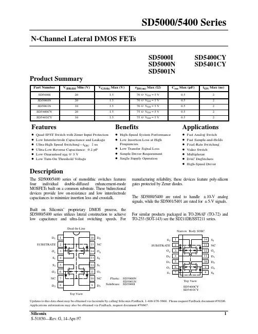
SD5000/5400 Series
Absolute Maximum Ratings (TA = 25_C Unless Otherwise Noted)
Benefits
D High-Speed System Performance D Low Insertion Loss at High Frequencies D Low Transfer Signal Loss D Simple Driver Requirement D Single Supply Operation
Specificationsa
Limits
SD5000 SD5400 SD5001 SD5401
Parameter Switching
Turn-On Turn On Time Turn-Off Turn Off Time
Symbolb
td(on) tr td(off) tf
Test Conditionsb
rDS(on)
VSB = 0 V ID = 1 mA
SD5400 Series VGS = 5 V VGS = 10 V VGS = 15 V VGS = 20 V
Resistance Match
DrDS(on)
VGS = 5 V
5
5
Dynamic
Forward Transconductance gf fs C(GS+GD+GB) C(GD+DB) C(GS+SB) Crss f= 3 kHz VDS = 10 V f = 1 MHz VGS = VBS = –15 V SD5000 Series VDS = 10 V VSB = 0 V ID = 20 mA f = 1 kHz SD5000 Series SD5400 Series 12 11 2.5 2.0 3.7 0.2 –107 10 9 3.5 3 5 0.5 10 mS 9 3.5 3 5 0.5 dB pF
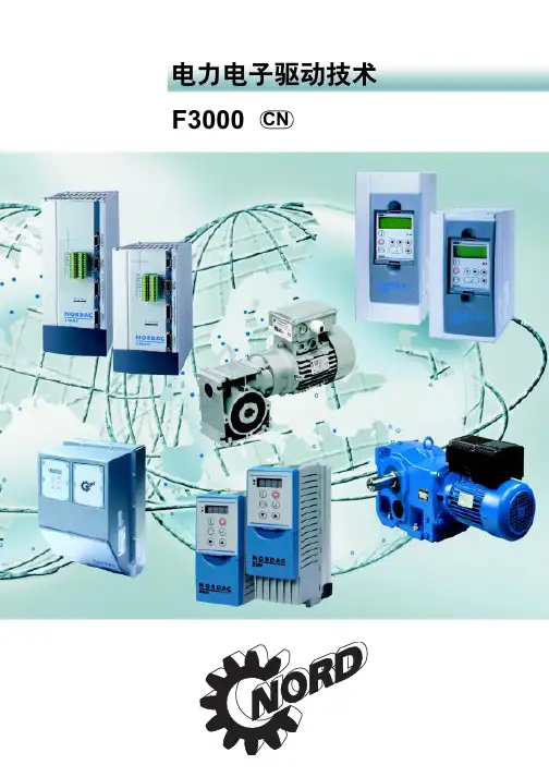
诺德全系列变频器资料F3000(中文)
160kW
!"#$
!
!"#$%&'()*+,!"#$% ! !"#$%&'()*+,!-./0 !"#$%
4
!"#$%&'() !"# 400% !A EMC !"#$%&' 22kW !" !" !"#$%!&'( !"#$%&'()* !"#$%& !"#$%&'()* !"#$%& !"#$%&'()*+,-
-750-323-A
-111-323-A
-151-323-A
-221-323-A
-301-323-A
-401-323-A
10% 47...63Hz 0.75kW 1hp 4.0 8.7/5.6 1.1kW 1 1/2hp 5.5 12.0/7.7 226 1.5kW 2hp 7.0 15.2/9.8 76 151 2.2kW 3hp 9.0 19.6/13.3 3.0kW 4hp 12.5 17.5 241 98 4kW 5hp 16.0 22.4 178
! "#$ ! "#
!"#$%&' ISD v/f ! 0 ! PTC I2t ...+40/50 !" !
IP20
-150-340-A 1.5kW/2hp 3.6A 6A
-221-340-A 2.2kW/3hp 5.2A 8A ! 123
-301-340-A 3.0kW/4hp 6.9A 3 11A
DS5000___安装配置手册v1.0
DS5000___安装配置手册v1.0DS5000安装配置手册v1.0目录一、DS5000磁阵配置 (3)1.磁盘规划 (3)2.连接磁盘阵列 (3)3.使用存储管理软件系统 (5)4.创建Array和LUN (11)5.创建第一个LUN (15)6.增加LUN (21)7.创建hotspare (21)二、将LUN映射给主机 (25)1.将磁盘柜与主机正确连接 (25)2.Lun与主机映射步骤: (26)3.在主机上使用lun创建VG,LV,FS (35)4.参数调整 (36)附录 (36)附录一:条带化建议 (36)附录二:-e’x’选项与-S选项说明 (37)本文档仅供研发内部使用,如需在生产环境使用,请先对指导书各步骤进行验证。
一、DS5000磁阵配置1.磁盘规划本次磁阵配置为16块硬盘的DS5020,采用RAID5建两个Array。
每个array包含8个盘。
每个array上建一个lun,分别是Omc1和Omc2。
在主机上分别对应为hdisk2、hdisk3。
分别将Omc1和Omc2分配到控制器A、B,以分担负荷。
2.连接磁盘阵列DS5020后板示意图其中Ethernet ports (以太网口)用于跟PC 连接,配置磁盘Serial port 串口Ethernet ports 以太网口Dual-port drive channel 扩展柜接口Fibre Channel host channels 主机接口DS5020有两个控制器:ControllerA 和ControllerB 。
每个控制器有一个网口,ControllerA的网口默认IP地址为192.168.128.101/255.255.255.0,ControllerB 的网口默认IP 地址为192.168.128.102/255.255.255.0。
控制台需要配置和DS5020控制器同一网段的IP 地址,用来连接DS502,此网段要求是一个独立的网络,不要加入其它的机器,以免IP 地址变更。
dsm UPS中文说明书
UPS说明书DSP6-1/1 DSP6-1/1-N DSP10-1/1 DSP10-1/1-N DSM10-3/1 DSM15-3/1 DSM20-3/1感谢您选用了CHAT UNION (捷联公司)的产品本文件内含有设备的操作信息任何人在开启UPS前,一定要仔细认真的阅读此文件1.…………………………………………………………….介绍1.1……………………………………………………………..型号介绍1.2……………………………………………………………..内部标记介绍2.………………………………………………………………安全说明3.………………………………………………………………安装说明3.1…………………………………………………………….拆包装及检测3.2…………………………………………………………….显示板说明3.3…………………………………………………………….外观及接口说明4.………………………………………………………………电路连接4.1…………………………………………………………….单机的连接4.2…………………………………………………………….并联机的连接5.………………………………………………………………操作说明5.1………………………………………………………………开机/关机5.2………………………………………………………………单机的操作说明5.3………………………………………………………………并联机的操作说明6.……………………………………………………………….远程通讯7.……………………………………………………………….故障及处理8.……………………………………………………………….指示灯和UPS的状态9.……………………………………………………………….生产标准10.…………………………………………………………….技术参数11.…………………………………………………………….服务热线12.……………………………………………………………...保修条款1.简介1.1型号介绍DSM系列UPS电源是采用双变换纯在线技术设计,可以保护您的设备免受来自市电的各种干扰。
SD05M50D(DS)说明书_1.0
反偏安全工作范围
符号
测试条件
最小值
BVDSS
VIN=0V,ID=250μA
(备注2) 500
ΔBVDSS/ΔTJ ID=250μA,相对于25°C点
-
IDSS
VIN=0V,VDS=500V
-
RDS(on) VCC=VBS=15V,VIN=5V,ID=1.2A
-
VSD
VCC=VBS=15V,VIN=0V,ID=-1.2A
Q176490316 136 7023 2221
内部框图
SD05M50D(DS)说明书
极限参数
参
数
加在P-N之间的电源电压 单 个 功 率 MOS 的 漏 极 持 续 电 流 , TC=25°C 单 个 功 率 MOS 的 漏 极 持 续 电 流 , TC=80°C 单个功率MOS的漏极峰值电流 TC=25°C, 脉冲宽度<100μs 最大功率耗散, TC=25°C 控制电源电压 高侧控制电压
#1
#16
1.30
4.43 2.48
2.80
#17 7.80
#23 15.60
LAND PATTERN RECOMMENDATIONS
12.30 17.90
(1.165) #1
0~0.2
0~0.2
15*1.778=26.67 ± 0.30
(13.335)
(13.335)
(1.85) (1.00) #16
13.5 13.5 3.0
0
1.2
-
典型值 300 15 15 -
-
15
最大值 400 16.5 16.5 VCC 0.8
-
-
单位 V V V V V
SD5501中文资料
N-Channel Depletion-Mode 4-Channel DMOS FET ArraySD5501FEATURES•Normally ON Configuration•Low Interelectrode Capacitances •High-Speed Switching•Wide Dynamic RangeAPPLICATIONS•High-Speed Analog Switches•Wide-Band Dual Differential Amplifiers •Dual Cascode Amplifiers•High Intercept Point Double Balanced Mixers DESCRIPTIONThe SD5501 is manufactured utilizing Calogic’s proprietary high speed, low capacitance DMOS process featuring an N-Channel depletion-mode design. This "normally-ON" device is well suited for high speed instrumentation and communication systems where multiple channels are required for fast switching or dual amplification. Available in a 16-pin plastic dual in-line plastic package or chip form.ORDERING INFORMATIONPart Package Temperature Range SD5501N Plastic-55C to +125C XSD5501Sorted Chips in Carriers-55o C to +125oCABSOLUTE MAXIMUM RATINGS (T A = +25o C unless otherwise noted)V DS Drain-Source Voltage. . . . . . . . . . . . . . . . . . . . +30 Vdc V SD Source-Drain Voltage. . . . . . . . . . . . . . . . . . . . +0.5 Vdc V DB Drain-Body Voltage. . . . . . . . . . . . . . . . . . . . . . +30 Vdc V SB Source-Body Voltage. . . . . . . . . . . . . . . . . . . . . +15 Vdc V GS Gate-Source Voltage. . . . . . . . . . . . . . . . . . . . . +25 Vdc V GB Gate-Body Voltage. . . . . . . . . . . . . . . . . . . . . . . +25 Vdc Gate-Body Voltage. . . . . . . . . . . . . . . . . . . . . . -0.3 Vdc V GD Gate-Drain Voltage. . . . . . . . . . . . . . . . . . . . . . +25 Vdc I D Continuous Drain Current. . . . . . . . . . . . . . . . . . 50 mA P D Total Package Power Dissipation(at or below TA = +25o C). . . . . . . . . . . . . . . . . 640 mW Linear Derating Factor. . . . . . . . . . . . . . . . 10.7 mW/o C P D Single Device Power Dissipation(at or below TA = +25o C). . . . . . . . . . . . . . . . . 300 mW Linear Derating Factor. . . . . . . . . . . . . . . . . 5.0 mW/o C T j Operating Junction Temperature Range. . -55 to +85o C T S Storage Temperature Range. . . . . . . . . -55 to + 150o CELECTRICAL CHARACTERISTCIS (T A = +25oC unless otherwise noted) Note 2: Match of 4 channels。
CP5008中文资料
CP
.034(.86) .030(.76)
Unit: inch ( mm )
.25(6.35)
.094(2.4) DIA
1.0(25.4) MAX
.442(11.23) .432(10.97)
1.135(28.8) 1.115(28.3) .672(17.1) .632(16.1)
FEATURES
• Electrically lsolated Metal Case for Maximum Heat Dissipation. • Surge Overload Ratings to 400 Amperes. • The plastic package has Underwriters Laboratory Flammability Classification 94V-O
60
40 30 20 15
60
50
40
10 8 6 4
30
20
10 0 25 60 80 100 120
O
5
10
15
20
25
30
35
50
140
160
180
AVERGE OUTPUT CURRENT,AMPERES
AMBIENT TEMPERATURE, T A C
Fig. 3- OUTPUT CURRENT VS. AMBIENT TEMPERATURE RESISTIVE OR INDUCTIVE LOAD BRIDGE MOUNTED ON A 8" x 8" ALUMINUM PLATE 25"THICK
Fig. 4- POWER DISSIPATION VS.AVERAGE OUTPUT CURRENT RESISTIVE OR INDUCTIVE LOAD TJ=150 OC
- 1、下载文档前请自行甄别文档内容的完整性,平台不提供额外的编辑、内容补充、找答案等附加服务。
- 2、"仅部分预览"的文档,不可在线预览部分如存在完整性等问题,可反馈申请退款(可完整预览的文档不适用该条件!)。
- 3、如文档侵犯您的权益,请联系客服反馈,我们会尽快为您处理(人工客服工作时间:9:00-18:30)。
General DescriptionThe DS5003 secure microprocessor incorporatessophisticated security features including an array ofmechanisms that are designed to resist all levels ofthreat, including observation, analysis, and physicalattack. As a result, a massive effort is required to obtainany information about its memory contents.Furthermore, the “soft” nature of the DS5003 allows fre-quent modification of the secure information, therebyminimizing the value of any secure information obtainedby such a massive effort. The device is an enhancedversion of the DS5002FP secure microprocessor chipwith additional scratchpad RAM.Differences from the DS5002FPThe DS5003 implements only one additional featurefrom the DS5002FP: it adds 128 bytes of internalscratchpad memory (for a total of 256 bytes) similar tothat used in 8032/8052 architectures. This additionalmemory is accessible through indirect addressing 8051instructions such as “mov a, @r1,” where r1 now canhave a value between 0 and 255. It is also usable asstack space for pushes, pops, calls, and returns. Register indirect addressing is used to access thescratchpad RAM locations above 7Fh. It can also beused to reach the lower RAM (0h–7Fh) if needed. Theaddress is supplied by the contents of the working reg-ister specified in the instruction. Thus, one instructioncan be used to reach many values by altering the con-tents of the designated working register. Note that onlyR0 and R1 can be used as pointers. An example of reg-ister indirect addressing is as follows:ANL A, @R0;Logical AND the Accumulator withthe contents of;the register pointed to by thevalue stored in R0ApplicationsPIN PadsGaming MachinesAny Application Requiring Software ProtectionFeatures♦8051-Compatible Microprocessor forSecure/Sensitive ApplicationsAccess 32kB, 64kB, or 128kB of NonvolatileSRAM for Program and/or Data Storage128 Bytes of RAM128 Bytes of Indirect Scratchpad RAMIn-System Programming Through On-ChipSerial PortCan Modify Its Own Program or Data Memory inthe End System
♦Firmware Security FeaturesMemory Stored in Encrypted FormEncryption Using On-Chip 64-Bit KeyAutomatic True Random-Key GeneratorSelf-Destruct Input (SDI)Top Coating Prevents MicroprobingProtects Memory Contents from Piracy
♦Crash-Proof OperationMaintains All Nonvolatile Resources for Over10 Years (at Room Temperature) in theAbsence of PowerPower-Fail ResetEarly Warning Power-Fail InterruptWatchdog Timer
DS5003Secure Microprocessor Chip
________________________________________________________________Maxim Integrated Products1Rev 0; 3/08
For pricing, delivery, and ordering information,please contact Maxim Directat 1-888-629-4642,or visit Maxim’s website at www.maxim-ic.com.
Pin Configuration appears at end of data sheet.Ordering Information+Denotes a lead-free/RoHS-compliant package.PART TEMP RANGE INTERNAL MICRO PROBE SHIELD PIN-PACKAGE
DS5003FPM-16+ 0°C to +70°C Yes 80 MQFP
元器件交易网www.cecb2b.comDS5003Secure Microprocessor Chip
2_______________________________________________________________________________________ABSOLUTE MAXIMUM RATINGS
DC CHARACTERISTICS(VCC= 5V ±10%, TA= 0°C to +70°C.)
Stresses beyond those listed under “Absolute Maximum Ratings” may cause permanent damage to the device. These are stress ratings only, and functionaloperation of the device at these or any other conditions beyond those indicated in the operational sections of the specifications is not implied. Exposure toabsolute maximum rating conditions for extended periods may affect device reliability.
Voltage Range on Any PinRelative to Ground..................................-0.3V to (VCC+ 0.5V)Voltage Range on VCCRelativeto Ground..........................................................-0.3V to +6.0VOperating Temperature Range.............................40°C to +85°CStorage Temperature*.......................................-55°C to +125°CSoldering Temperature...........................Refer to the IPC/JEDECJ-STD-020 Specification.
PARAMETER SYMBOL CONDITIONS MIN TYP MAX UNITS Operating Voltage VCC (Note 1) VCCMIN 5.5 V Minimum Operating Voltage VCCMIN 0°C to +70°C (Note 1) 4.00 4.12 4.25 V Power-Fail Warning Voltage VPFW 0°C to +70°C (Note 1) 4.25 4.37 4.50 V Lithium Supply Voltage VLI (Note 1) 2.5 4.0 V Operating Current at 16MHz ICC (Note 2) 36 mA Idle-Mode Current at 12MHz IIDLE 0°C to +70°C (Note 3) 7.0 mA Stop-Mode Current ISTOP (Note 4) 80 μA Pin Capacitance CIN (Note 5) 10 pF