● Routing geometries
穿越活动断裂带隧道抗错断措施研究

1.1 工程概况 通麦隧道位于西藏自治区南部东段波密县通麦
镇,整体上沿 G318国道北侧展布,与国道相距最远处 约 3.7km.进口为茶隆隆巴曲左岸,道路交通不便,出 口为通麦小集镇.隧道洞身段不良地质类型较多,分 别为岩爆、大变形、高地温、活动断裂、高瓦斯气体等. 最新地质资料显示,洞身强烈岩爆段 800m,50~60 ℃中高温段 2580m,二级大变形段 135m,高瓦斯气 体 855m以及近出口段穿越 415m长活动断裂带, 隧道出口端与通麦车站相连,该区域地形地貌受到 区域地质构造的控制,山脉总体走向与构造迹线一 致,总体地势北高南低,地形起伏较大.通麦隧道地
8
兰州交通大学学报
第 40卷
根据中国国家铁路集团有限公司的总体安排及 规划,川藏铁路东部起始于四川省成都市,向西途径 雅安、康定、昌都、林芝,西止于西藏拉萨,新建线路 总长度大约为 1567.37km[1],川藏铁路沿线地震活 动强烈、地 震 频 发,是 影 响 工 程 安 全 的 主 要 地 质 灾 害,自有记载以来,至少发生了 7级以上地震 22次 以上[2].国内 外 诸 多 案 例 表 明,穿 越 活 动 断 裂 带 隧 道极其容易产生严重的破坏[3?5].活动断层的运动分 为粘滑运动和蠕滑运动,活动断层从粘结到瞬间发 生滑移的这一过程被称为粘滑,与其相对应的另外 一种相对运动较为缓慢的方式叫蠕滑,二者区别就 在于蠕滑没有从粘结到瞬间发生滑移,引起地层发 生瞬时的脆性断裂,而是以较稳定的速率蠕动,粘滑 运动导致的脆性断裂会在瞬间释放巨大能量,引起 地震.而川藏线沿线的有诸多活动断裂带,根据目前 的勘探结果显示,多数断裂兼具走滑和逆冲的活动 性质[6],且具 有 明 显 的 年 平 均 位 移 速 率,虽 然 蠕 滑 导致的两盘相对位移较小,但随着时间不断累积,对 隧道结构的安全性仍有威胁.
GOOD_Paper_A 60-GHz CMOS Receiver Front-End_Razavi
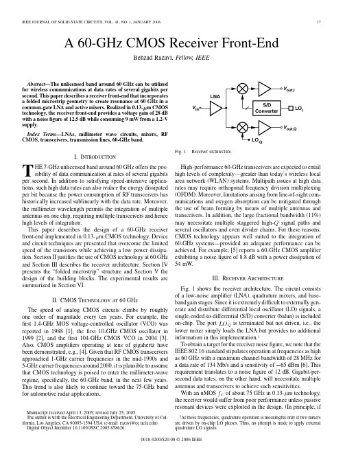
A 60-GHz CMOS Receiver Front-EndBehzad Razavi ,Fellow,IEEEAbstract—The unlicensed band around 60GHz can be utilized for wireless communications at data rates of several gigabits per second.This paper describes a receiver front-end that incorporates a folded microstrip geometry to create resonance at 60GHz in a common-gate LNA and active mixers.Realized in0.13-m CMOS technology,the receiver front-end provides a voltage gain of 28dB with a noise figure of 12.5dB while consuming 9mW from a 1.2-V supply.Index Terms—LNAs,millimeter wave circuits,mixers,RF CMOS,transceivers,transmission lines,60-GHz band.I.I NTRODUCTIONTHE 7-GHz unlicensed band around 60GHz offers the pos-sibility of data communication at rates of several gigabits per second.In addition to satisfying speed-intensive applica-tions,such high data rates can also reduce the energy dissipated per bit because the power consumption of RF transceivers has historically increased sublinearly with the data rate.Moreover,the millimeter wavelength permits the integration of multiple antennas on one chip,requiring multiple transceivers and hence high levels of integration.This paper describes the design of a 60-GHz receiver front-end implemented in0.13-m CMOS technology.Device and circuit techniques are presented that overcome the limited speed of the transistors while achieving a low power dissipa-tion.Section II justifies the use of CMOS technology at 60GHz and Section III describes the receiver architecture.Section IV presents the “folded microstrip”structure and Section V the design of the building blocks.The experimental results are summarized in Section VI.II.CMOS T ECHNOLOGY AT 60GHzThe speed of analog CMOS circuits climbs by roughly one order of magnitude every ten years.For example,the first 1.4-GHz MOS voltage-controlled oscillator (VCO)was reported in 1988[1],the first 10-GHz CMOS oscillator in 1999[2],and the first 104-GHz CMOS VCO in 2004[3].Also,CMOS amplifiers operating at tens of gigahertz have been demonstrated,e.g.,[4].Given that RF CMOS transceivers approached 1-GHz carrier frequencies in the mid-1990s and 5-GHz carrier frequencies around 2000,it is plausible to assume that CMOS technology is poised to enter the millimeter-wave regime,specifically,the 60-GHz band,in the next few years.This trend is also likely to continue toward the 75-GHz band for automotive radar applications.Manuscript received April 13,2005;revised July 25,2005.The author is with the Electrical Engineering Department,University of Cal-ifornia,Los Angeles,CA 90095-1594USA (e-mail:razavi@).Digital Object Identifier10.1109/JSSC.2005.858626Fig.1.Receiver architecture.High-performance 60-GHz transceivers are expected to entail high levels of complexity—greater than today’s wireless local area network (WLAN)systems.Multipath issues at high data rates may require orthogonal frequency division multiplexing (OFDM).Moreover,limitations arising from line-of-sight com-munications and oxygen absorption can be mitigated through the use of beam forming by means of multiple antennas and transceivers.In addition,the large fractional bandwidth (11%)may necessitate multiple staggeredhigh-signal paths and several oscillators and even divider chains.For these reasons,CMOS technology appears well suited to the integration of 60-GHz systems—provided an adequate performance can be achieved.For example,[5]reports a 60-GHz CMOS amplifier exhibiting a noise figure of 8.8dB with a power dissipation of 54mW.III.R ECEIVER A RCHITECTUREFig.1shows the receiver architecture.The circuit consists of a low-noise amplifier (LNA),quadrature mixers,and base-band gain stages.Since it is extremely difficult to externally gen-erate and distribute differential local oscillator (LO)signals,a single-ended-to-differential (S/D)converter (balun)is includedon-chip.Theportis terminated but not driven,i.e.,the lower mixer simply loads the LNA but provides no additional information in this implementation.1To obtain a target for the receiver noise figure,we note that the IEEE 802.16standard stipulates operation at frequencies as high as 60GHz with a maximum channel bandwidth of 28MHz for a data rate of 134Mb/s and a sensitivity of 65dBm [6].This requirement translates to a noise figure of 12dB.Gigabit-per-second data rates,on the other hand,will necessitate multiple antennas and transceivers to achieve such sensitivities.With annMOSof about 75GHz in0.13-m technology,the receiver would suffer from poor performance unless passive resonant devices were exploited in the design.(In principle,if1Atthese frequencies,quadrature operation is meaningful only if two mixers are driven by on-chip LO phases.Thus,no attempt is made to apply external quadrature LO signals.0018-9200/$20.00©2006IEEEFig.2.(a)Folded microstrip and (b)its narrowband equivalentcircuit.Fig.3.Dependence of folded microstrip parameters upon linewidth:(a)inductance and capacitance;(b)parallel resistance and Q ;(c)maximum absorbable capacitance and parallelresisance.resonates with an inductor having a quality factorof ,thenthe rises by the same factor.)While spiral inductors have proved useful at tens of gigahertz,their performance at 60GHz may be inadequate due to substrate eddy currents.Such currentsequivalently introduce aresistance,,in parallel with the in-ductor,thereby limitingtheat high frequencies.More importantly,the magnetic coupling to the substrate signi fi-cantly alters the inductance value at these frequencies,requiring detailed knowledge of the substrate pro file if an accurate model is to be developed.In contrast to spiral inductors,transmission lines (T-lines)substantially con fine the electric and magnetic fields and hence better lend themselves to modeling.For example,T-lines ex-hibita relatively independent of the length and hence the in-ductance value,whereas spiral geometries do not.Nevertheless,the necessary length of such lines (several hundred microns)leads to disproportionately tall layouts,making the routing of the signal and power lines dif ficult.Coplanar lines in CMOS technology,introduced in [2],have been characterized for frequencies up to 50GHz [5].This work incorporates microstrip structures as they interact negligibly with the substrate and can be modeled more accurately.IV .F OLDED M ICROSTRIPIn order to alleviate routing dif ficulties,this design incorpo-rates a “folded ”microstrip geometry.Shown in Fig.2(a),the structure is realized as a metal 8signal line over a metal 1ground plane.With the two ends of the line near each other,the layout of the receiver is greatly simpli fied.(A somewhat similar topology has been used in [7].)For circuit design,the structure is modeled by the lumped tank depicted in Fig.2(b),a justi fied approximation because the total length of the line is about one-tenth of the wavelength.22Underthis condition,the structure can be tuned by means of varactors toaccomodate a greater bandwith.RAZA VI:A 60-GHz CMOS RECEIVER FRONT-END19Fig.4.(a)Example of current distribution in folded microstrip.(b)Current distributions for different leg separations.(c)Resistance and inductance variation as a function of S .Using the electromagnetic field simulatorSONNET,is computed at three frequencies at and around 60GHz and theresults are used to determine the equivalent valuesof,,and.3For a given length,the folded microstrip of Fig.2(a)provides two parameters that affect the performance:thelinewidth and the spacing between thelegs .Fig.3(a)and (b)plots the tankparametersasvaries from3m to12m while the length of each leg is155mand m.Asexpected,falls,rises,increases to some extent,and improves.For ampli ficationpurposes,must be maximizedandand must be minimized so that the tank can absorb maximum transistor capacitance while resonating at 60GHz.The plot in Fig.3(c)quanti fies these requirements,indicatingdiminishing returnsasexceeds6m.Thus,a linewidth of6m is used in this work.The spacing between the two legs also plays a critical role in the design.Forsmall ,the mutual magnetic coupling lowers the overall inductance,thus degrading the performance of the line.Fig.4(a)depicts the distribution of the current as predicted by SONNET.4(Darker shades correspond to higher densities.)Based on these simulations,the current distribution in each leg(along theline)can be plotted for different valuesof [Fig.4(b)].As expected,greater valuesof reduce the cur-rent density at the inner edges.From the circuit design pointof view,we again consider the variationofandwith [Fig.4(c)],notingthat reaches a relatively constant value3Note that the self-resonance frequency of the structure is well above 60GHz.4Thedistributions are not exactly symmetric because one port of the foldedmicrostrip isgrounded.Fig.5.(a)Cascode and (b)common-gate LNA topologies.for m (about twice the linewidth).5Thus,this valueofis chosen in this work.V .B UILDING B LOCKSA.LNA DesignFig.5shows two candidates for the LNA design.At frequen-cies well belowthe of the transistors,the cascode topology of Fig.5(a)provides a low noise figure,good input matching,and a high reverse isolation.At 60GHz,on the other hand,the poleat the drainof(typically on the orderof )shunts a con-siderable portion of the RF current to ground,thereby loweringthe gain and raising the noise contributedby.Furthermore,the small degeneration and gate series inductances (50–100pH)required for input matching make the circuit very sensitive to package parasitics.5TheQ varies only slightly here,from 10.3to 12.2.20IEEE JOURNAL OF SOLID-STA TE CIRCUITS,VOL.41,NO.1,JANUARY2006Fig.6.LNA circuitdiagram.Fig.7.Simulated LNA characteristics.The above observations suggest that the LNA must contain a single transistor before voltage ampli fication occurs,naturally pointing to the common-gate (CG)stage of Fig.5(b).However,the required50-input resistance translates to a large transistor width(20m)and hence about 35fF of input capacitance,de-grading both the input match and the noise figure.That is,the capacitance seen at the source node must be cancelled by means of resonance.Similarly,the output node must also resonate so as to cancel the capacitance seen at the drain and introduced by the next stage.Moreover,the noise contributedby raises the noise figure considerably.Fig.6shows the LNA implementation,whereresonateswithand the pad capacitance,and with the total capacitance atnode .Transistorprovides additional gain and drive capability for the subsequent quadrature mixers.The three inductors are realized as the folded microstrip de-picted in Fig.2(a).With an equivalent parallel resistance ofabout700,contributes negligible noise.It is desirable to avoid AC coupling between the two stages of the LNA and between the LNA and the mixers.Metal-sandwich capacitors suffer from large bottom-plate parasitics,and lateral fringe structures may exhibit resonances close to the band of interest.A biasing scheme is introduced here that obviates the need for coupling capacitors.In the circuit of Fig.6,transistorserves as a diode-connected device,carrying a current equalto.Thus,if the DC dropsacrossand are negli-gible,forms a current mirror along with the common-source devices in the next stage,de fining the bias current of the mixers.Due to the physical dimensions of the folded microstrips in the layout,the LNA output must travel35m before reaching the mixers.This interconnect is modeled by the simple network in the dashed box shown in Fig.6.Fig.7plots thesimulatedFig.8.(a)Conventional and (b)proposed mixertopologies.Fig.9.Simulated noise figure for two mixer topologies.voltage gain and noise figure of the LNA across the unlicensed band.The tradeoff between the maximum gain and the band-width suggests that varactor tuning of the LNA may be neces-sary.The circuit draws a supply current of 4mA.B.MixerFig.8shows the conventional and proposed mixer topolo-gies.According to simulations,the circuit of Fig.8(a)exhibits a noise figure of 26dB and a conversion gain of 0dB.Several mechanisms account for this poor performance.First,the totalcapacitance at the drainofgives rise to a pole on the orderof .Second,sinceand must carry the entire biascurrentof,they switch quite gradually,inject noise to the output,and “waste ”part of the RF current as a common-mode component.Third,the limited supply voltage allows only a small voltage drop across the load resistors and hence a low conversion gain.To alleviate these issues,we introduce the topology depictedin Fig.8(b),whereinductor(a folded microstrip)resonates with the total capacitance seen at the drainof and also car-ries about half of the drain currentof.Now,most of the RF current is commutatedbyand because the equivalent parallel resistanceof is much greater than the average resis-tance seen looking into the sources of the switching pair.(For thesame reason,the thermal noise contributedby is negligible.)Moreover,carrying a smallercurrent,and switch more abruptly.Finally,the load resistors can be doubled.As a result,the noise figure falls to about 18dB and the conversion gain rises to 12dB.The mixer core draws 0.9mA.Fig.9plots the noise figure of the two topologies across the unlicensed band.In bothcases,and .RAZA VI:A 60-GHz CMOS RECEIVER FRONT-END21Fig.10.Balunrealization.Fig.11.Receiver floor plan.C.BalunAs mentioned in Section III,a balun is included on the chip to facilitate testing.Shown in Fig.10,the circuit consists oftwo equal couplingcapacitorsand (realized as metal sandwiches)and aninductor(implemented as a folded microstrip).For,(1)(2)The balancebetweenand is degraded to some extent by the input capacitance of the mixer and the parasiticsof .D.Output BufferThe output buffer consists of a simple differential pair fol-lowed by open-drain common-source devices that can drive50-instrumentation.The targeted voltage gain is about 12dB to ensure the receiver output noise overwhelms the noise floor of spectrum analyzers and noise figure meters.As such,the buffer exhibits a (simulated)1-dB compression point of about100mV(equivalent to 7dBm in a50-system)and tends to limit the linearity of the receiver.VI.E XPERIMENTAL R ESULTSThe receiver front-end has been designed and fabricated in digital0.13-m CMOS technology.Fig.11shows the floor plan.Note that the folded microstrips allow placement of the ac-tive devices in close proximity,with only one long interconnect(35m).Also,the wide ground planes under the microstrips serve as a low-impedance return path throughout the chip.Fig.12depicts the die,whose active area measures400m300m.The circuit has been tested on a Cascade probe station while operating with a 1.2-V supply.Since 60-GHz cablesandFig.12.Die photograph.TABLE IM EASURED P ERFORMANCE OF RECEIVERFig.13.Input/output characteristic of the front-end.probes suffer from a high loss,an on-chip pad frame is used to measure the loss of two back-to-back sets of cables and probes.Table I summarizes the measured performance of the receiver.The gain is measured as follows.The signal level provided by the 60-GHz generator is measured by means of an accurate power meter and subsequently applied to the circuit through a variable attenuator.The downconverted signal is monitored on a spectrum analyzer,and the measured loss of the input cable and probe is taken into account.Fig.13plots the input/output characteristic.The noise figure is measured using two approaches.6In the first approach,a 60-GHz signal with a level of 35dBm (mea-sured accurately by a power meter and a variable attenuator)is applied to the receiver.The input SNR in 1Hz is thus equaltodBmdBm dBm.The downconverted signal at an intermediate frequency of 100MHz is then displayed on a spectrum analyzer and the output SNR in 1Hz is measured.The loss of the input cable and probe is then subtracted from the difference between these SNRs (all in dB)to obtain the noise figure.6Noshield room was available for these measurements.22IEEE JOURNAL OF SOLID-STA TE CIRCUITS,VOL.41,NO.1,JANUARY2006Fig.14.V oltage gain and noise figure.e of two antennas and receivers to reduce noise figure.In the second approach,a 60-GHz noise generator and a stan-dard noise figure meter are used.The two methods yield nearly the same results.Fig.14plots the voltage gain and noise figure across the unlicensed band.The voltage gain and the noise figure are,respectively,8dB lower and 4dB higher than simulated values.The source of these discrepancies is unknown at this point but LO imbalance due to the balun and noise picked up by the probe station are possible causes.VII.C ONCLUSIONCMOS technology is poised to enter the millimeter-wave regime and supplant many III-V circuits.This paper has inves-tigated the properties of folded microstrips for ampli fication at 60GHz and introduced new CMOS LNA and mixer topologies that exploit resonant devices to operate at high frequencies.A receiver front-end employing these concepts achieves a noise figure of 12.5dB and a gain of 28dB while consuming 9mW.The remarkably low power dissipation and small area of the receiver offer interesting possibilities for higher performance.For example,suppose two antennas and two receivers are inte-grated as shown in Fig.15.Even without sophisticated antenna diversity and beam forming techniques,the baseband voltages of the two receivers can be added to improve the signal-to-noise ratio by 3dB with a total power dissipation of less than 20mW.Note that phase coherence at the two antennas (at 60GHz)is not critical;only the baseband data streams must have a reasonable phase alignment.A CKNOWLEDGMENTThe author wishes to thank A.Parsa for his valuable assistance.R EFERENCES[1]M.Banu,“MOS oscillators with multi-decade tuning range and giga-hertz maximum speed,”IEEE J.Solid-State Circuits ,vol.23,no.6,pp.1386–1393,Dec.1988.[2] B.Kleveland et al.,“Monolithic CMOS distributed ampli fier and oscil-lator,”in IEEE ISSCC Dig.Tech.Papers ,Feb.1999,pp.70–71.[3]L.M.Franca-Neto,R.E.Bishop,and B.A.Bloechel,“64-GHz and100-GHz VCO ’s in 90-nm CMOS using optimum pumping method,”in IEEE ISSCC Dig.Tech.Papers ,Feb.2004,pp.444–445.[4] F.Ellinger,“26-42GHz SOI CMOS low noise ampli fier,”IEEE J.Solid-State Circuits ,vol.39,no.3,pp.522–528,Mar.2004.[5] C.H.Doan et al.,“Millimeter-wave CMOS design,”IEEE J.Solid-StateCircuits ,vol.40,no.1,pp.144–155,Jan.2005.[6]IEEE Std 802.162004,IEEE Standard for Local and Metropolitan AreaNetworks,Part 16:Air Interface for Fixed Broadband Wireless Access Systems ,2004.[7]H.Li and H.M.Rein,“Millimeter-wave VCOs with wide tuning rangeand low phase noise,fully integrated in a SiGe bipolar production tech-nology,”IEEE J.Solid-State Circuits ,vol.38,no.2,pp.184–191,Feb.2003.Behzad Razavi (S ’87–M ’90–SM ’00–F ’03)received the B.Sc.degree in electrical engineering from Sharif University of Technology,Tehran,Iran,in 1985and the M.Sc.and Ph.D.degrees in electrical engineering from Stanford University,Stanford,CA,in 1988and 1992,respectively.He was with AT&T Bell Laboratories and Hewlett-Packard Laboratories until 1996.Since 1996,he has been Associate Professor and subse-quently Professor of electrical engineering at the University of California,Los Angeles.His currentresearch includes wireless transceivers,frequency synthesizers,phase-locking and clock recovery for high-speed data communications,and data converters.He was an Adjunct Professor at Princeton University from 1992to 1994,and at Stanford University in 1995.He is the author of Principles of Data Conversion System Design (IEEE Press,1995),RF Microelectronics (Prentice-Hall,1998)(translated into Chinese and Japanese),Design of Analog CMOS Integrated Circuits (McGraw-Hill,2001)(translated into Chinese and Japanese),and Design of Integrated Circuits for Optical Communications (McGraw-Hill,2003),and the editor of Monolithic Phase-Locked Loops and Clock Recovery Circuits (IEEE Press,1996),and Phase-Locking in High-Performance Systems (IEEE Press,2003).Prof.Razavi served on the Technical Program Committees of the Interna-tional Solid-State Circuits Conference (ISSCC)from 1993to 2002and VLSI Circuits Symposium from 1998to 2002.He has also served as Guest Editor and Associate Editor of the IEEE J OURNAL OF S OLID -S TATE C IRCUITS ,IEEE T RANSACTIONS ON C IRCUITS AND S YSTEMS ,and the International Journal of High Speed Electronics .He received the Beatrice Winner Award for Editorial Excellence at the 1994ISSCC,the Best Paper Award at the 1994European Solid-State Circuits Conference,the Best Panel Award at the 1995and 1997ISSCC,the TRW Innovative Teaching Award in 1997,and the Best Paper Award at the IEEE Custom Integrated Circuits Conference in 1998.He was the co-re-cipient of both the Jack Kilby Outstanding Student Paper Award and the Beatrice Winner Award for Editorial Excellence at the 2001ISSCC.He was also recog-nized as one of the top 10authors in the 50-year history of ISSCC.He is an IEEE Distinguished Lecturer and a Fellow of IEEE.。
机械专业英语

机械专业英语词汇(很全)金属切削 metal cutting 切削深度 cutting depth机床 machine tool 前刀面 rake face金属工艺学 technology of metals 刀尖 nose of tool刀具 cutter 前角 rake angle摩擦 friction 后角 clearance angle联结 link 龙门刨削 planing传动 drive/transmission 主轴 spindle轴 shaft 主轴箱 headstock弹性 elasticity 卡盘 chuck频率特性 frequency characteristic 加工中心 machining center 误差 error 车刀 lathe tool响应 response 车床 lathe定位 allocation 钻削 镗削 bore机床夹具 jig 车削 turning动力学 dynamic 磨床 grinder运动学 kinematic 基准 benchmark静力学 static 钳工 locksmith分析力学 analyse mechanics 锻 forge拉伸 pulling 压模 stamping压缩 hitting 焊 weld剪切 shear 拉床 broaching machine扭转 twist 拉孔 broaching弯曲应力 bending stress 装配 assembling强度 intensity 铸造 found三相交流电 three-phase AC 流体动力学 fluid dynamics 磁路 magnetic circles 流体力学 fluid mechanics 变压器 transformer 加工 machining异步电动机 asynchronous motor 液压 hydraulic pressure 几何形状 geometrical 切线 tangent精度 precision 稳定性 stability正弦形的 sinusoid 介质 medium交流电路 AC circuit 液压驱动泵 fluid clutch 机械加工余量 machining allowance 液压泵 hydraulic pump变形力 deforming force 阀门 valve变形 deformation 失效 invalidation应力 stress 强度 intensity硬度 rigidity 载荷 load热处理 heat treatment 应力 stress退火 anneal 安全系数 safty factor正火 normalizing 可靠性 reliability脱碳 decarburization 螺纹 thread渗碳 carburization 螺旋 helix电路 circuit 键 spline半导体元件 semiconductor element 销 pin反馈 feedback 滚动轴承 rolling bearing发生器 generator 滑动轴承 sliding bearing直流电源 DC electrical source 弹簧 spring门电路 gate circuit 制动器 arrester brake逻辑代数 logic algebra 十字结联轴节 crosshead外圆磨削 external grinding 联轴器 coupling内圆磨削 internal grinding 链 chain平面磨削 plane grinding 皮带 strap变速箱 gearbox 精加工 finish machining离合器 clutch 粗加工 rough machining绞孔 fraising 变速箱体 gearbox casing绞刀 reamer 腐蚀 rust螺纹加工 thread processing 氧化 oxidation螺钉 screw 磨损 wear铣削 mill 耐用度 durability铣刀 milling cutter 随机信号 random signal功率 power 离散信号 discrete signal工件 workpiece 超声传感器 ultrasonic sensor齿轮加工 gear mechining 集成电路 integrate circuit齿轮 gear 挡板 orifice plate主运动 main movement 残余应力 residual stress主运动方向 direction of main movement 套筒 sleeve进给方向 direction of feed 扭力 torsion进给运动 feed movement 相图 phase diagram合成进给运动 resultant movement of feed 热处理 heat treatment合成切削运动 resultant movement of cutting 固态相变 solid state phase changes合成切削运动方向 direction of resultant movement of cutting 有色金属 nonferrous metal机电一体化 mechanotronics mechanical-electrical integration 陶瓷 ceramics气压 air pressure pneumatic pressure 合成纤维 synthetic fibre冷加工 cold machining 电化学腐蚀 electrochemical corrosion电动机 electromotor 车架 automotive chassis汽缸 cylinder 悬架 suspension过盈配合 interference fit 转向器 redirector热加工 hotwork 变速器 speed changer摄像头 CCD camera 板料冲压 sheet metal parts倒角 rounding chamfer 孔加工 spot facing machining优化设计 optimal design 车间 workshop工业造型设计 industrial moulding design 工程技术人员 engineer有限元 finite element 气动夹紧 pneuma lock滚齿 hobbing 数学模型 mathematical model插齿 gear shaping 画法几何 descriptive geometry伺服电机 actuating motor 机械制图 Mechanical drawing铣床 milling machine 投影 projection钻床 drill machine 视图 view镗床 boring machine 剖视图 profile chart步进电机 stepper motor 标准件 standard component丝杠 screw rod 零件图 part drawing导轨 lead rail 装配图 assembly drawing组件 subassembly 尺寸标注 size marking可编程序逻辑控制器 Programmable Logic Controller PLC 技术要求 technical requirements电火花加工 electric spark machining 刚度 rigidity电火花线切割加工 electrical discharge wire - cutting 动能 kinetic energy内力 internal force 势能 potential energy位移 displacement 机械能守恒 conservation of mechanical energy 截面 section 动量 momentum疲劳极限 fatigue limit 桁架 truss断裂 fracture 轴线 axes塑性变形 plastic distortion 余子式 cofactor脆性材料 brittleness material 逻辑电路 logic circuit刚度准则 rigidity criterion 触发器 flip-flop垫圈 washer 脉冲波形 pulse shape垫片 spacer 数模 digital analogy直齿圆柱齿轮 straight toothed spur gear 液压传动机构 fluid drive mechanism 斜齿圆柱齿轮 helical-spur gear 机械零件 mechanical parts直齿锥齿轮 straight bevel gear 淬火冷却 quench运动简图 kinematic sketch 淬火 hardening齿轮齿条 pinion and rack 回火 tempering蜗杆蜗轮 worm and worm gear 调质 hardening and tempering虚约束 passive constraint 磨粒 abrasive grain曲柄 crank 结合剂 bonding agent摇杆 racker 砂轮 grinding wheel凸轮 cams 曲率 curvature共轭曲线 conjugate curve 偏微分 partial differential范成法 generation method 毛坯 rough定义域 definitional domain 游标卡尺 slide caliper值域 range 千分尺 micrometer calipers导数\\微分 differential coefficient 攻丝 tap求导 derivation 二阶行列式 second order determinant 定积分 definite integral 逆矩阵 inverse matrix不定积分 indefinite integral 线性方程组 linear equations排列组合 permutation and combination 概率 probability气体状态方程 equation of state of gas 随机变量 random variable塑件模具相关英文compre sion molding压缩成型 runner system浇道系统flash mold溢流式模具 stress crack应力电裂plsitive mold挤压式模具 orientation定向split mold分割式模具 sprue gate射料浇口,直浇口 cavity型控 母模 nozzle射嘴core模心 公模 sprue lock pin料头钩销(拉料杆) taper锥拔 slag well冷料井leather cloak仿皮革 side gate侧浇口shiver饰纹 edge gate侧缘浇口flow mark流痕 tab gate搭接浇口welding mark溶合痕 film gate薄膜浇口post screw insert螺纹套筒埋值 flash gate闸门浇口self tapping screw自攻螺丝 slit gate缝隙浇口striper plate脱料板 fan gate扇形浇口piston活塞 dish gate因盘形浇口cylinder汽缸套 diaphragm gate隔膜浇口chip细碎物 ring gate环形浇口handle mold手持式模具 subarine gate潜入式浇口 encapsulation molding低压封装成型、射出成型用模具 tunnel gate隧道式浇口two plate两极式(模具) pin gate针点浇口well type蓄料井 Runner less无浇道insulated runner绝缘浇道方式 (sprue less)无射料管方式hot runner热浇道 long nozzle延长喷嘴方式runner plat浇道模块 sprue浇口;溶渣valve gate阀门浇口 eject pin顶出针band heater环带状的电热器 knock pin顶出销spindle阀针 return pin回位销反顶针spear head刨尖头 sleave套筒slag well冷料井 stripper plate脱料板cold slag冷料渣 insert core放置入子air vent排气道 runner stripper plate浇道脱料板 welding line熔合痕guide pin导销subzero深冷处理 three plate三极式模具机械设计及周边其他用语英汉对照assembly drawing 装配图 auto tool change cycle 自动换刀时间周期 beam 横梁 bending moment 弯矩bending stress 弯曲应力 bottoming 底靠buckling 纵弯曲 chamfering 去角斜切channel 凹槽 chattering 颤动check point 查核点 chip 切屑chip conveyor 排屑输送机 coefficient of friction 摩擦系数 compact 小型的 cooling pipe 冷却管coupon 试样胚 deflection 挠曲量distortion 扭曲变形 draft taper 拔模锥度draw out 拉拔 fit tolerance 配合公差flexible rigidity 弯曲刚性 gas vent 气孔hatching 剖面线 heater cooler 加热器冷却装置hook cavity 钩穴 inching 寸动lug 凸缘 maintenance 维修保固metallurgy 冶金学 notch effect 切口效果out of roughness 真圆度 performance 动作性能pit 坑 plane strain 倒角应力plug mill 蕊棒轧管机 repeated load 重覆载荷riveted joint ?钉接合 sand paper 砂纸shift 偏移 shrink fit 热压配合shrinkage hole 缩孔 sinking 凹陷sketch 草图 spalling 剥落straightness 直度 submarine 深陷式surface roughness 表面粗度 tapping 攻螺丝thermocouple 热电耦 torsion load 扭转载荷toughness 韧性 tracing 描图under cut 凹割机床行业英汉对照1(1):按英文字母排序 3-Jaws indexing spacers 三爪、分割工具头 CNC engraving machines 电脑数控雕刻机A.T.C.system 加工中心机刀库 CNC grinding machines 电脑数控磨床 Aluminum continuous melting & holding furnaces 连续溶解保温炉 CNC lathes 电脑数控车床Balancing equipment 平衡设备 CNC machine tool fittings 电脑数控机床配件 Bayonet 卡口 CNC milling machines 电脑数控铣床Bearing fittings 轴承配件 CNC shearing machines 电脑数控剪切机 Bearing processing equipment 轴承加工机 CNC toolings CNC刀杆Bearings 轴承 CNC wire-cutting machines 电脑数控线切削机 Belt drive 带传动 Conveying chains 输送链Bending machines 弯曲机 Coolers 冷却机Blades 刀片 Coupling 联轴器Blades,saw 锯片 Crimping tools 卷边工具Bolts,screws & nuts 螺栓,螺帽及螺丝 Cutters 刀具Boring heads 搪孔头 Cutting-off machines 切断机Boring machines 镗床 Diamond cutters 钻石刀具Cable making tools 造线机 Dicing saws 晶圆切割机Casting,aluminium 铸铝 Die casting dies 压铸冲模Casting,copper 铸铜 Die casting machines 压铸机Casting,gray iron 铸灰口铁 Dies-progressive 连续冲模Casting,malleable iron 可锻铸铁 Disposable toolholder bits 舍弃式刀头 Casting,other 其他铸造 Drawing machines 拔丝机Casting,steel 铸钢 Drilling machines 钻床Chain drive 链传动 Drilling machines bench 钻床工作台Chain making tools 造链机 Drilling machines,high-speed 高速钻床 Chamfer machines 倒角机 Drilling machines,multi-spindle 多轴钻床 Chucks 夹盘 Drilling machines,radial 摇臂钻床 Clamping/holding systems 夹具/支持系统 Drilling machines,vertical 立式钻床CNC bending presses 电脑数控弯折机 drills 钻头CNC boring machines 电脑数控镗床Electric discharge machines(EDM) 电火花机 CNC drilling machines 电脑数控钻床 Electric power tools 电动刀具CNC EDM wire-cutting machines 电脑数控电火花线切削机 Engraving machines 雕刻机CNC electric discharge machines 电脑数控电火花机 Engraving machines,laser 激光雕刻机 Etching machines 蚀刻机 Laser cutting 激光切割Finishing machines 修整机 Laser cutting for SMT stensil 激光钢板切割机Fixture 夹具 Lathe bench 车床工作台Forging dies 锻模 Lathes,automatic 自动车床Forging,aluminium 锻铝 Lathes,heavy-duty 重型车床Forging,cold 冷锻 Lathes,high-speed 高速车床Forging,copper 铜锻 Lathes,turret 六角车床Forging,other 其他锻造 Lathes,vertical 立式车床Forging,steel 钢锻 Lubricants 润滑液Foundry equipment 铸造设备 Lubrication Systems 润滑系统Gear cutting machines 齿轮切削机 Lubricators 注油机Gears 齿轮 Machining centers,general 通用加工中心Gravity casting machines 重力铸造机 Machining centers,horizontal 卧式加工中心Grinder bench 磨床工作台 Machining centers,horizontal & vertical 卧式及立式加工中心 Grinders,thread 螺纹磨床 Machining centers,vertical 立式加工中心Grinders,tools & cutters 工具磨床 Machining centers,vertical double-column type 立式双柱加工中心 Grinders,ultrasonic 超声波打磨机 Magnetic tools 磁性工具Grinding machines 磨床 Manifolds 集合管Grinding machines,centerless 无心磨床 Milling heads 铣头Grinding machines,cylindrical 外圆磨床 Milling machines 铣床Grinding machines,universal 万能磨床 Milling machines,bed type 床身式铣床Grinding tools 磨削工具 Milling machines,duplicating 仿形铣床Grinding wheels 磨轮 Milling machines,horizontal 卧式铣床Hand tools 手工具 Milling machines,turret vertical 六角立式铣床Hard/soft and free expansion sheet making plant 硬(软)板(片)材及自由发泡板机组Heat preserving furnaces 保温炉 Milling machines,universal 万能铣床Heating treatment funaces 熔热处理炉 Milling machines,vertical 立式铣床Honing machines 搪磨机 Milling machines,vertical & horizontal 立式及卧式铣床Hydraulic components 液压元件Hydraulic power tools 液压工具Hydraulic power units 液压动力元件Hydraulic rotary cylinders 液压回转缸Jigs 钻模Lapping machines 精研机Lapping machines,centerless 无心精研机常用加工机械3D coordinate measurement 三次元量床 boring machine 搪孔机cnc milling machine CNC铣床 contouring machine 轮廓锯床copy grinding machine 仿形磨床 copy lathe 仿形车床copy milling machine 仿形铣床 copy shaping machine 仿形刨床cylindrical grinding machine 外圆磨床 die spotting machine 合模机drilling machine ?孔机 engraving machine 雕刻机engraving E.D.M. 雕模放置加工机 form grinding machine 成形磨床graphite machine 石墨加工机 horizontal boring machine 卧式搪孔机horizontal machine center 卧式加工制造中心 internal cylindrical machine 内圆磨床 jig boring machine 冶具搪孔机 jig grinding machine 冶具磨床lap machine 研磨机 machine center 加工制造中心multi model miller 靠磨铣床 NC drilling machine NC钻床NC grinding machine NC磨床 NC lathe NC车床NC programming system NC程式制作系统 planer 龙门刨床profile grinding machine 投影磨床 projection grinder 投影磨床radial drilling machine 旋臂?床 shaper 牛头刨床surface grinder 平面磨床 try machine 试模机turret lathe 转塔车床 universal tool grinding machine 万能工具磨床vertical machine center 立式加工制造中心 wire E.D.M. 线割放电加工机冲压机械及周边关连用语英汉对照back shaft 支撑轴 blank determination 胚料展开 hand press 手动冲床 hand rack pinion press 手动齿轮齿条式冲床 bottom slide press 下传动式压力机 board drop hammer 板落锤 hand screw press 手动螺旋式冲床 hopper feed 料斗送料brake 煞车 buckle 剥砂面 idle stage 空站 inching 微调尺寸camlachie cramp 铸包 casting on flat ?合 isothermal forging 恒温锻造 key clutch 键槽离合器chamotte sand 烧磨砂 charging hopper 加料漏斗 knockout 脱模装置 knuckle mechanic 转向机构clearance 间隙 closed-die forging 合模锻造 land 模具直线刀面部 level 水平clump 夹紧 clutch 离合器 loader 供料器 unloader 卸料机clutch brake 离合器制动器 clutch boss 离合器轮壳 loop controller 闭回路控制器 lower die 下模clutch lining 离合器覆盖 coil car 带卷升降运输机 micro inching device 微寸动装置 microinching equipment 微动装置 coil cradle 卷材进料装置 coil reel stand 钢材卷料架 motor 马达 moving bolster 活动工作台column 圆柱 connection screw 连杆调节螺钉 notching press 冲缺口压力机 opening 排料逃孔core compound 砂心黏结剂 counter blow hammer 对击锻锤 overload protection device 防超载装置 pinch roll 导正滚轮 cradle 送料架 crank 曲柄轴 pinion 小齿轮 pitch 节距crankless 无曲柄式 cross crank 横向曲轴 pressfit 压入 progressive 连续送料cushion 缓冲 depression 外缩凹孔 pusher feed 推杆式送料 pusher feeder 料片押片装置dial feed 分度送料 die approach 模口角度 quick die change system 快速换模系统 regrinding 再次研磨die assembly 合模 die cushion 模具缓冲垫 releasing 松释动作 reversed blanking 反转下料die height 冲压闭合高度 die life 模具寿命 robot 机器人 roll forming machine 辊轧成形die opening 母模逃孔 die spotting press 调整冲模用压力机 roll forming machine 辊轧成形机 roll release 脱辊double crank press 双曲柄轴冲床 draght angle 逃料倾斜角 roller feed 辊式送料 roller leveler 辊式矫直机edging 边锻伸 embedded core 加装砂心 rotary bender 卷弯成形机 safety guard 安全保护装置feed length 送料长度 feed level 送料高度 scrap cutter 废料切刀 scrap press 废料冲床filling core 埋入砂心 filling in 填砂 seamless forging 无缝锻造 separate 分离film play 液面花纹 fine blanking press 精密下料冲床 shave 崩砂 shear angle 剪角forging roll 辊锻机 finishing slag 炼後熔渣 sheet loader 薄板装料机 shot 单行程工作fly wheel 飞轮 fly wheel brake 飞轮制动器 shrinkage fit 收缩配合 shut height 闭合高度foot press 脚踏冲床 formboard 进模口板 sieve mesh 筛孔 sintering of sand 铸砂烧贴frame 床身机架 friction 摩擦 slide balancer 滑动平衡器 slug hole 逃料孔friction brake 摩擦煞车 gap shear 凹口剪床 spin forming machine 旋压成形机 spotting 合模gear 齿轮 gib 滑块引导部 stack feeder 堆叠拨送料机 stickness 黏模性gripper 夹具 gripper feed 夹持进料 straight side frame 冲床侧板 stretcher leveler 拉伸矫直机 gripper feeder 夹紧传送装置 hammer 槌机 strip feeder 料材送料装置 stripping pressure 弹出压力stroke 冲程 take out device 取料装置toggle press 肘杆式压力机 transfer 传送transfer feed 连续自动送料装置 turrent punch press 转塔冲床two speed clutch 双速离合器 uncoiler 闭卷送料机unloader 卸载机 vibration feeder 振动送料机wiring press 嵌线卷边机机械工具英语机械工具 spanner 扳子 (美作:wrench) double-ended spanner 双头扳子adjustable spanner, monkey wrench 活扳子,活络扳手box spanner 管钳子 (美作:socket wrench) calipers 卡规pincers, tongs 夹钳 shears 剪子 hacksaw 钢锯wire cutters 剪线钳 multipurpose pliers, universal pliers 万能手钳 adjustable pliers 可调手钳 punch 冲子 drill 钻 chuck 卡盘scraper 三角刮刀 reamer 扩孔钻 calliper gauge 孔径规rivet 铆钉 nut 螺母 locknut 自锁螺母,防松螺母 bolt 螺栓半自动化 semi-automation; semi-automatic 扳手 wrenchpin, peg, dowel 销钉 washer 垫圈 staple U形钉车床 lathe; turning lathe 车刀 lathe tooloil can 油壶 jack 工作服 grease gun 注油枪车轮车床 car wheel lathe 车削 turning 车轴 axle机械加工 拋光 polishing 安装 to assemble 衬套 bushing柄轴 arbor 部件 units; assembly parts 插床 slotting machine半机械化 semi-mechanization; semi-mechanized备件 spare parts 边刨床 side planer 变速箱 transmission gear半自动滚刀磨床 semi-automatic hob grinder拆卸 to disassemble 超高速内圆磨床 ultra-high-speed internal grinder心装置。
英文常用术语
英文常用术语PIE Process Integration Engineer(工艺整合工程师)工艺能力technology硅片(wafer)基材(substrate)工艺过程(module)工艺过程(module)主要有四个部分:DIFF(扩散)、TF(薄膜)、PHOTO(光刻)、ETCH(刻蚀)。
其中DIFF又包括FURNACE(炉管)、WET(湿刻)、IMP(离子注入)、RTP(快速热处理)。
TF包括PVD(物理气相淀积)、CVD(化学气相淀积) 、CMP(化学机械研磨)。
光罩层数(mask layer) Poly(多晶硅) metal(金属导线)start oxide 的目的①不希望有机成分的光刻胶直接碰触Si 表面。
②在laser刻号过程中,亦可避免被产生的粉尘污染。
为何需要zero layer?答:芯片的工艺由许多不同层次堆栈而成的, 各层次之间以zero layer当做对准的基准。
Laser mark是什么用途? Wafer ID 又代表什么意义?答:Laser mark 是用来刻wafer ID, Wafer ID 就如同硅片的身份证一样,一个ID代表一片硅片的身份。
ID是英文Identity code的缩写,身份标识号码的意思。
也可以称为序列号或帐号,是某个体系中相对唯一的编码,相当于是一种“身份证”。
13. 一般硅片的制造(wafer process)过程包含哪些主要部分?答:①前段(frontend)-元器件(device)的制造过程。
②后段(backend)-金属导线的连接及护层(passivation)14. 前段(frontend)的工艺大致可区分为那些部份?答:①STI的形成(定义AA区域及器件间的隔离)②阱区离子注入(well implant)用以调整电性③栅极(poly gate)的形成④源/漏极(source/drain)的形成⑤硅化物(salicide)的形成15. STI 是什么的缩写? 为何需要STI?答:STI: Shallow Trench Isolation(浅沟道隔离),STI可以当做两个组件(device)间的阻隔, 避免两个组件间的短路.16. AA 是哪两个字的缩写? 简单说明AA 的用途?答:Active Area, 即有源区,是用来建立晶体管主体的位置所在,在其上形成源、漏和栅极。
机加工行业常用英语词汇

机加工行业常用英语词汇学习Aabrasion?n.?磨料,研磨材料,磨蚀剂,?a.?磨损的,磨蚀的abrasive?belt?n.?砂带abrasive?belt?grinding?n.?砂带磨削,用研磨带磨光abrasive?cut-off?machine?n.?砂轮切断机abrasive?dressing?wheel?n.?砂轮修整轮abrasive?grain?n.?磨料粒度abrasive?grit?n.?研磨用磨料,铁粒abrasive?lapping?wheel?n.?磨料研磨轮accuracy?of?position?n.?位置精度accuracy?to?shape?n.?形状精度active?cutting?edge?n.?主切削刃adapter?flange?n.?连接器法兰盘adjointing?flanks?n.?共轭齿廓align?n.?找中(心),找正,对中,对准,找平,调直,校直,调整,调准angle?milling?cutter?n.?角铣刀angular?grinding?n.?斜面磨削,斜磨法angular?milling?n.?斜面铣削angular?plunge?grinding?n.?斜向切入磨削angular?turning?n.?斜面车削arbour?n.?刀杆,心轴,柄轴,轴,辊轴attachment?n.?附件,附件机构,联结,固接,联结法automatic?bar?machine?n.?棒料自动车床automatic?boring?machine?n.?自动镗床automatic?copying?lathe?n.?自动仿形车床automatic?double-head?milling?machine?n.?自动双轴铣床automatic?lathe?n.?自动车床automatic?turret?lathe?n.?自动转塔车床Bbelt?grinding?machine?n.?砂带磨床bench?lathe?n.?台式车床bevel?n.?斜角,斜面,倾斜,斜切,斜角规,万能角尺,圆锥的,倾斜的,斜边,伞齿轮,锥齿轮bevel?gear?cutting?machine?n.?锥齿轮切削机床bevel?gear?tooth?system?n.?锥齿轮系,锥齿轮传动系统borehole?n.?镗孔,镗出的孔,钻眼boring?n.?镗孔,钻孔,穿孔??boring?fixture?n.?镗孔夹具boring?machine?n.?镗床boring?tool?n.?镗刀boring,?drilling?and?milling?machine?n.?镗铣床broaching?machine?n.拉床,铰孔机,剥孔机broaching?tool?n.?拉刀broad?finishing?tool?n.?宽刃精切刀,宽刃精车刀,宽刃光切刀Ccalibrate?vt.?校准〔正〕,刻度,分度,检查〔验〕,定标,标定,使标准化,使符合标准cam?contour?grinder?n.?凸轮仿形磨床carbide?tip?n.?硬质合金刀片carbide?turning?tool?n.?硬质合金车刀carbide-tipped?tool?n.?硬质合金刀具cast?iron?machining?n.?铸铁加工,铸铁切削加工centerless?cylindrical?grinder?n.?无心外圆磨床ceramic?cutting?tool?n.?金属陶瓷刀具chamfer?n.;vt.?倒角,倒棱chamfered?cutting?edge?n.?倒角刀刃champing?fixture?n.?快换夹具champing?jaw?n.?快换卡爪chaser?n.?螺纹梳刀,梳刀盘,板牙chatter?vi.;n.?振动,振荡,震颤,刀振chip?n.?切屑,铁屑,刀片,刀头,片,薄片,芯片,基片chip?breaker?groove?radius?n.?断屑槽底半径,卷屑槽底半径chip?clearance?n.?切屑间隙chip?cross-sectional?area?n.?切屑横截面面积chip?curl?n.?螺旋形切屑chip?flow?n.?切屑流chip?formation?n.?切屑形成chip?removing?process?n.?去毛刺加工chip?variable?n.?切屑变量chuck?n.?卡盘,夹盘,卡头,〔电磁〕吸盘,vt.?固定,装卡,夹紧,卡住chucker?n.?卡盘车床,卡角车床circular?drillling?machine?n.?圆工作台钻床circular?path?n.?环路,圆轨迹circular?pitch?measurement?n.?周节测量circumference?n.?圆周,周线,周界,周围,四周,范围close-grained?a.?细颗粒的coeffecient?of?tool?thrust?n.?刀具推力系数coil?chip?n.?卷状切屑cold?circular?saw?n.?冷圆锯cold?saw?n.?冷锯column?drilling?machine?n.?圆〔方〕柱立式钻床combined?drill?and?milling?cutter?n.?复合钻铣床complete?traverse?grinding?n.?横进给磨削,切入磨削computer-controlled?machine?n.?计算机控制机床,数控机床?contact?pattern?n.?靠模continuous?chip?n.?连续切屑continuous?spiral?chip?n.?连续螺旋切屑contour?n.?轮廓,外形,外貌,轮廓线,回路,网路,电路,等高线,等值线,轮廓等高距?a.?仿形的,靠模的contour?milling?n.?成形铣削,外形铣削,等高走刀曲面仿形法convex?milling?attachment?n.?凸面铣削附件convex?turning?attachment?n.?中凸车削附件,凸面车削附件coolant?lubricant?n.?冷却润滑剂coolant?lubricant?emulsion?n.?冷却润滑乳液〔剂〕copy?n.?样板,仿形,靠模工作法,拷贝复制品,?v.?复制,模仿,抄录copy?grinding?n.?仿形磨床copy-mill?n.?仿形铣copying?turret?lathe?n.?仿形转塔车床corner?n.?角,弯〔管〕头,弯管counterbore?n.?埋头孔,沉孔,锥口孔,平底扩孔钻,平底锪钻,?n.;vt.?扩孔,锪孔,镗孔,镗阶梯孔crankshaft?grinding?machine?n.?曲轴磨床crankshaft?turning?lathe?n.?曲轴车床creep?feed?grinding?n.?缓进给磨削cross?milling?n.?横向铣削curly?chip?n.?卷状切屑,螺旋形切屑,切屑螺旋cut?v.;n.?切削〔割〕,口,片,断,断开,削减,减少,断面,剖面,相交,凹槽cut?off?n.?切断〔开,去〕,关闭,停车,停止,断开装置,断流器,挡板,截止,截流cut?teeeth?n.?铣齿cut-off?grinding?n.?砂轮截断,砂轮切割cutter?n.?刀具,切削工具,截断器,切断器,切断机cutting?n.?切削,切片,切割,切屑,金属屑,截槽cutting?edge?profile?n.?切削刃轮廓〔外形,断面〕,切削刃角度cutting?force?n.?切削力cutting?lip?n.?切削刃,刀刃,钻唇,钻刃cutting?operation?n.?切削加工,切削操作,切削作业cutting?rate?n.?切削效率,切削速率cutting?tool?n.?刀具,切削工具,刃具cycle?n.?周期,周,循环,一个操作过程,轮转,自行车cylindrical?grinder?n.?外圆磨床Ddeep-hole?drilling?n.深孔钻削deep-hole?milling?n.?深孔铣削design?n.?设计,计算,计划,方案,设计书,图纸die-sinking?n.?凹模dimension?n.?尺寸,尺度,维度,量纲,因次direction?of?the?feed?motion?n.?进给方向,进刀方向discontinuous?chip?n.?间断切屑??distance?n.?距离,间隔〔隙〕,长度,vt.?隔开double-column?planer-miller?n.?双柱龙门铣床dress?v.?修饰,修整,平整,整理,清理,装饰,调制,准备,打磨,磨光,压平,轿直,清洗,清理,分级drilling?n.?钻头,钻床,穿孔器,凿岩机,v.?钻孔,打孔,钻井,钻探drilling?machine?n.?钻床,钻机,钻孔机,打眼机drilling?tool?n.?钻孔〔削,井,眼〕工具Eedge?point?n.?刀口,刀刃external?grinding?n.?外圆磨削Fface?n.?表面,外观,工作面,表盘,屏,幕?v.?面向,朝向,表面加工,把表面弄平face?grinding?machine?n.?平面磨床face?milling?machine?n.?端面磨床feed?force?n.?进给力feed?motion?n.?进给运动fine?adjustment?n.?精调,细调,微调fine?boring?n.?精密镗孔??finish?v.;n.?精加工,抛光,修整,表面粗糙度,完工,最后加工,最后阶段,涂层,涂料finish-cutting?n.?精加工,最终切削fixture?n.?夹具,夹紧装置,配件,零件,定位器,支架form?n.?型式,类型,摸板,模型,形成,产生,成形,表格?v.?形〔组,构〕成,产生,作出,成形,造型form-turn?n.?成形车削free-cutting?n.?自由切削,无支承切削,高速切削Ggap?n.?间隔,间隙,距离,范围,区间,缺口,开口火花隙,?vt.?使产生裂缝?vi.?豁开gear?cutting?machine?n.?齿轮加工机床,切齿机gear?generating?grinder?n.?磨齿机gear?hob?n.?齿轮滚刀grinding?cutter?n.?磨具grinding?force?n.?磨削力grinding?machine?n.?磨床grinding?wheel?diameter?n.?砂轮直径grinding?wheel?width?n.?砂轮宽度groove?n.?槽,切口,排屑槽,空心槽,坡口,vt.?切〔开,铣〕槽groove?milling?n.铣槽Hheadstock?spindle?n.?床头箱主轴,主轴箱主轴,头架轴helical?tooth?system?n.?螺旋齿轮传动装置high?precision?lathe?n.?高精度车床high-speed?n.?高速high-speed?machining?n.?高速加工hob?n.?齿轮滚刀,滚刀,螺旋铣刀,v.?滚铣,滚齿,滚削horsepower?n.?马力hobbing?machine?n.?滚齿机,螺旋铣床,挤压制模压力机,反应阴模机hole?n.?孔,洞,坑,槽,空穴,孔道,管道,v.?钻〔穿,冲,开〕孔,打洞hone?n.?vt.?磨石,油石,珩磨头,磨孔器,珩磨,honing?machine?n.?珩磨机,珩床,搪磨床,磨孔机,磨气缸机Iinclination?n.?倾斜,斜度,倾角,斜角〔坡〕,弯曲,偏〔差,角〕转increment?n.?增量,增加,增〔大〕长indexing?table?automatic?n.?自动分度工作台?infeed?grinding?n.?切入式磨削installation?n.?装置,设备,台,站,安装,设置internal?grinding?n.?内圆磨削involute?hob?n.?渐开线滚刀jig?boring?machine?n.?坐标镗床Kkeyway?cutting?n.?键槽切削加工knurling?tool?n.?滚花刀具,压花刀具,滚花刀Llaedscrew?machine?n.?丝杠加工机床lap?grinding?n.?研磨lapping?n.?研磨,抛光,精研,搭接,擦准lathe?n.?车床lathe?dog?n.?车床轧头,卡箍,鸡心夹头,离心夹头,制动爪,车床挡块lathe?tool?n.?车刀level?n.?水平,水准,水平线,水平仪,水准仪,电平,能级,程度,强度,a.?水平的,相等的,均匀的,平稳的loading?time?n.?装载料时间,荷重时间,充填时间,充气时间lock?n.?锁,栓,闸,闭锁装置,锁型,同步,牵引,v.?闭锁,关闭,卡住,固定,定位,制动刹住longitudinal?grinding?n.?纵磨low?capacity?machine?n.?小功率机床〔机器〕Mmachine?axis?n.?机床中心线machine?table?n.?机床工作台machine?tool?n.?机床,工作母机machining?n.?机械加工,切削加工machining?(or?cutting)?variable?n.?加工(或切削)变量machining?allowance?n.?机械加工余量machining?cycle?n.?加工循环machining?of?metals?n.?金属切削加工,金属加工magazine?automatic?n.?自动化仓库,自动化料斗,自动存贮送料装置manufacture?n.?制造者,生产者,厂商,产品,制造material?removing?rate?n.?材料去除率metal?cutting?n.?金属切削metal-cutting?technology?n.?金属切削工艺学,金属切削工艺〔技术〕metal-cutting?tool?n.?金属切削刀具,金属切削工具micrometer?adjustment?n.?微调milling?n.?铣削,磨碎,磨整,选矿milling?feed?n.?铣削进给,铣削走刀量,铣削走刀机构milling?machine?n.?铣床milling?spindle?n.?铣床主轴milling?tool?n.?铣削刀具,铣削工具mount?v.?固定,安装,装配,装置,架设,n.?固定件,支架,座,装置,机构mounting?n.?安装,装配,固定,机架,框架,装置mounting?fixture?n.?安装夹具,固定夹具Nnose?n.?鼻子,端,前端,凸头,刀尖,机头,突出部分,伸出部分number?of?revolutions?n.?转数numerical?control?n.?数控numerically?controlled?lathe?n.?数控车床oblique?grinding?n.?斜切式磨床operate?v.?操纵,控制,运行,工作,动作,运算operating?cycle?n.?工作循环operation?n.?运转,操作,控制,工作,作业,运算,计算operational?instruction?n.?操作说明书,操作说明operational?safety?n.?操作安全性,使用可靠性oscillating?type?abrasive?cutting?machine?n.?摆动式砂轮切割机oscillation?n.?振动,振荡,摆动,颤振,振幅out-cut?milling?n.?切口铣削oxide?ceramics?n.?氧化物陶瓷oxide-ceramic?cutting?tool?n.?陶瓷刀具Pperformance?n.?实行,执行,完成,特性,性能,成品,制作品,行为,动作,生产率,效率peripheral?grinding?n.?圆周磨削peripheral?speed?n.?圆周速度,周速,边缘速度perpendicular?a.?垂直的,正交的,成直角的?n.?垂直,正交,竖直,垂线,垂直面physical?entity?n.?实体,实物pitch?n.?齿距,节距,铆间距,螺距,极距,辊距,坡度,高跨比,俯仰角pitch?circle?n.?节圆plain?(or?cylindrical)?milling?machine?n.?普通(或圆柱形)铣床plain?grinding?n.?平面磨削plain?turning?n.?平面车床plane?n.?平面,面,投影,刨,水平,程度,阶段,飞机?a.平的?v.?弄平,整平,刨,飞行plane?milling?n.?平面铣削plane-mill?n.?平面铣刀,平面铣床plunge?mill?n.?模向进给滚轧机plunge-cut?n.?切入式磨削,横向进给磨削,全面进刀法,全面进给法plunge-cut?thread?grinder?n.?切入式螺纹磨床plunge-grinding?n.?切入式磨削point?n.?点,尖端,刀尖,针尖,指针,交点,要点,论点,特点?v.?指,面向,瞄准,对准,表明,弄尖,强调power?n.?功率,效率,能〔容,力〕量,动力,电源,能源?v.?驱〔拖,带,发〕动,给...以动力power?hacksaw?n.?机动弓锯〔钢锯〕precision?boring?n.?精镗precision?boring?machine?n.?精密镗床precision?machining?n.?精密机械加工pressure?angle?n.?压力角primary?cutting?edge?n.?主切削刃principal?feed?motion?n.?主进给运动,主进刀运动production?method?s?n.?生产方法[式]profile?n.?轮廓,形面,剖面,侧面图,分布图。
ASTM D3763
Designation:D 3763–02Standard Test Method forHigh Speed Puncture Properties of Plastics Using Load and Displacement Sensors 1This standard is issued under the fixed designation D 3763;the number immediately following the designation indicates the year of original adoption or,in the case of revision,the year of last revision.A number in parentheses indicates the year of last reapproval.A superscript epsilon (e )indicates an editorial change since the last revision or reapproval.1.Scope *1.1This test method covers the determination of puncture properties of plastics,including films,over a range of test velocities.1.2Test data obtained by this test method is relevant and appropriate for use in engineering design.1.3The values stated in SI units are to be regarded as the standard.1.4This standard does not purport to address all of the safety concerns,if any,associated with its use.It is the responsibility of the user of this standard to establish appro-priate safety and health practices and determine the applica-bility of regulatory limitations prior to use.N OTE 1—This specification does not closely conform to ISO 6603.2.The only similarity between the two tests is that they are both instru-mented impact tests.The differences in striker,fixture,and specimen geometries and in test velocity can produce significantly different test results.2.Referenced Documents 2.1ASTM Standards:D 618Practice for Conditioning Plastics and Electrical Insulating Materials for Testing 2D 883Terminology Relating to Plastics 2D 1600Terminology for Abbreviated Terms Relating to Plastics 2D 4000Classification System for Specifying Plastic Mate-rials 3E 691Practice for Conducting an Interlaboratory Study to Determine the Precision of a Test Method 42.2ISO Standard:5ISO 6603.2Plastics—Determination of Multiaxial Impact Behavior of Rigid Plastics Part 2:Instrumented Puncture Test3.Terminology3.1Definitions —For definitions see Terminology D 883and for abbreviations see Terminology D 1600.4.Significance and Use4.1This test method is designed to provide load versus deformation response of plastics under essentially multiaxial deformation conditions at impact velocities.This test method further provides a measure of the rate sensitivity of the material to impact.4.2Multiaxial impact response,while partly dependent on thickness,does not necessarily have a linear correlation with specimen thickness.Therefore,results should be compared only for specimens of essentially the same thickness,unless specific responses versus thickness formulae have been estab-lished for the material.4.3For many materials,there may be a specification that requires the use of this test method,but with some procedural modifications that take precedence when adhering to the specification.Therefore,it is advisable to refer to that material specification before using this test method.Table 1of Classi-fication System D 4000lists the ASTM materials standards that currently exist.5.Interferences5.1Inertial Effects —A loading function encountered when performing an instrumented impact test that may,in some cases,confuse the interpretation of the test data.For further definition and examples of inertial effects,refer to Appendix X1.6.Apparatus6.1The testing machine shall consist of two assemblies,one fixed and the other driven by a suitable method to achieve the required impact velocity (that is,hydraulic,pneumatic,me-chanical,or gravity):6.1.1Clamp Assembly,consisting of two parallel rigid plates with a 76.063.0mm diameter hole in the center of each.The hole edges shall be rounded to a radius of 0.860.4mm.Sufficient force must be applied (mechanically,pneumati-cally,or hydraulically)to prevent slippage of the specimen in1This test method is under the jurisdiction of ASTM Committee D20on Plastics and is the direct responsibility of Subcommittee D20.10on Mechanical Properties.Current edition approved December 10,2002.Published February 2003.Origi-nally approved in st previous edition approved in 2000as D 3763-00.2Annual Book of ASTM Standards,V ol 08.01.3Annual Book of ASTM Standards,V ol 08.02.4Annual Book of ASTM Standards,V ol 14.02.5Available from American National Standards Institute (ANSI),25W.43rd St.,4th Floor,New York,NY 10036.1*A Summary of Changes section appears at the end of this standard.Copyright ©ASTM International,100Barr Harbor Drive,PO Box C700,West Conshohocken,PA 19428-2959,United States.Copyright ASTM InternationalReproduced by IHS under license with ASTMLicensee=Lear - Southfield/5910410001 Not for Resale, 04/26/2005 15:39:59 MDTNo reproduction or networking permitted without license from IHS--``,,`````,,`,``````,`,`,,-`-`,,`,,`,`,,`---the clamp during impact.Iffilms are tested,some type of gasket may also be required to prevent slippage.6.1.2Plunger Assembly,consisting of a12.7060.13mm diameter steel rod with a hemispherical end of the same diameter positioned perpendicular to,and centered on,the clamp hole.6.1.3Other Geometries—The dimensions given in6.1.1 and6.1.2shall be the standard geometry.If other plunger or hole sizes are used they shall be highlighted in the report. Correlations between various geometries have not been estab-lished.6.1.4Load Sensing System—A load cell of sufficiently high natural resonance frequency,as described in A1.1,used to-gether with a calibrating network for adjusting load sensitivity.6.1.5Plunger Displacement Measurement System—A means of monitoring the displacement of the moving assembly during the loading and complete penetration of the specimen. This can be accomplished through the use of a suitable transducer or potentiometer attached directly to the system. Photographic or optical systems can also be utilized for measuring displacement.6.1.5.1Alternatively,displacement may be calculated as a function of velocity and total available energy at initial impact, along with increments of load versus time,using a micropro-cessor.6.1.5.2Some machines use an accelerometer,whose output is used to calculate both load and displacement.6.1.6Display and Recording Instrumentation—Use any suitable means to display and record the data developed from the load and displacement-sensing systems,provided its re-sponse characteristics are capable of presenting the data sensed,with minimal distortion.The recording apparatus shall record load and displacement simultaneously.For further information,see A1.2.6.1.6.1The most rudimentary apparatus is a cathode-ray oscilloscope with a camera.This approach also requires a planimeter or other suitable device,capable of measuring the area under the recorded load-versus-displacement trace of the event with an accuracy of65%.6.1.6.2More sophisticated systems are commercially avail-able.Most of them include computerized data reduction and automatic printouts of results.7.Test Specimen7.1Specimens must be large enough to be adequately gripped in the clamp.In general,the minimum lateral dimen-sion should be at least13mm greater than the diameter of the hole in the clamp(see6.1.1and10.9).7.2Specimens may be cut from injection-molded,extruded, or compression molded sheet;or they may be cast or molded to size.8.Conditioning8.1Conditioning—Condition the test specimens in a room or enclosed space maintained2362°C,and50%relative humidity,in accordance with Procedure A in Practice D618 unless otherwise specified.8.2Test Conditions—Conduct tests in the standard labora-tory atmosphere of2362°C,and5065%relative humidity,unless otherwise specified.In cases of disagreement,the tolerances shall be61°C,and62%relative humidity.8.2.1By changing the conditioning and test temperature ina controlled manner for a given test velocity,the temperature at which transition from ductile to brittle failure occurs can be determined for most plastics.N OTE2—To facilitate high throughput during automated testing at temperatures other than ambient,it is often necessary to stack the specimens in a column with no airflow in between.To assure compliance with Section10of Practice D618,the time to equilibrium must be determined for a given material.A thermocouple may be placed at the center of a specimen stack in which its height is equal to its minimum width.Determine the time to reach equilibrium at the desired test temperature.Experiments with materials having low thermal conductivity values have shown that more than7.5h of soak time was required before the stack center temperature fell within the tolerances specified in D618 at a setpoint of-40°C.Two and a half additional hours were needed to reach equilibrium.The opposite extreme was seen in a material of higher thermal conductivity that only required2h to reach equilibrium at-40°C.9.Speed of Testing9.1For recommended testing speeds see10.4.10.Procedure10.1Test a minimum offive specimens at each specified speed.10.2Measure and record the thickness of each specimen to the nearest0.025mm at the center of the specimen.10.3Clamp the specimen between the plates of the speci-men holder,taking care to center the specimen for uniform gripping.Tighten the clamping plate in such a way as to provide uniform clamping pressure to prevent slippage during testing.10.4Set the test speed to the desired value.The testing speed(movable-member velocity at the instant before contact with the specimen)shall be as follows:10.4.1For single-speed tests,use a velocity of200m/min.10.4.1.1Other speeds may be used,provided they are clearly stated in the report.10.4.2To measure the dependence of puncture properties on impact velocity,use a broad range of test speeds.Some suggested speeds are2.5,25,125,200,and250m/min. 10.5Set the available energy so that the velocity slowdown is no more than20%from the beginning of the test to the point of peak load.If the velocity should decrease by more than 20%,discard the results and make additional tests on new specimens with more available energy.N OTE3—It is observed that when the available energy is at least three times the absorbed energy at the peak load velocity slow-down is less than 20%.10.6Place a safety shield around the specimen holder. 10.7Make the necessary adjustments to data collection apparatus as required by the manufacturer’s instructions or consult literature such as STP9366for further information regarding setting up data acquisition systems.6Instrumented Impact Testing of Plastics and Composite Materials,ASTM STP 936,ASTM,1986.10.8Conduct the test,following the manufacturer’s instruc-tions for the specific equipment used.10.9Remove the specimen and inspect the gripped portion for striations or other evidence of slippage.If there is evidence of slippage,modify the clamping conditions or increase the specimen size and repeat test procedures.11.Calculation11.1Using the load-versus-displacement trace and appro-priate scaling factors,calculate the following:11.1.1Peak load,in newtons.11.1.2Deflection,in millimetres,to the point where peak loadfirst occurred.11.1.3From the area within the trace,calculate:11.1.3.1Energy,in joules,to the point where loadfirst occurred.11.1.3.2Total energy absorbed.The point for determining this has not been standardized.Therefore,the point used for each test must be stated in the report.11.1.4Load,deflection,energy,or combination thereof,at any other specific point of interest(see Appendix X1).11.2For each series of tests,calculate the arithmetic mean for each of the above,to three significantfigures.11.3Calculate the estimated standard deviations as follows:S5S S X22n X2n21D1/2(1) where:S=estimated standard deviation,X=value of a single determination,n=number of determinations,andX=arithmetic mean of the set of determinations.12.Report12.1Report the following information:12.1.1Complete identification of the material tested,includ-ing type,source,manufacturer’s code number,form and previous history,12.1.2Specimen size and thickness,12.1.3Method of preparing test specimens(compression molding,casting,etc.),12.1.4Geometry of clamp and plunger,if different from 6.1.1and6.1.2,12.1.5Source and types of equipment,12.1.6Speed of testing(see10.4),12.1.7The point on the curve at which total energy was calculated(see11.1.3.2),12.1.8Average value and standard deviation for each of the properties listed in11.1,12.1.9Whether or not any slippage of the specimens was detected,and12.1.10If the effect of testing speeds was studied(see 10.4.2).13.Precision and Bias13.1Tables1-3are based on a round robin conducted in 1996in accordance with Practice E691,involving7materials tested by11laboratories.For each material,all of the speci-mens were prepared at the laboratory of the company volun-teering that material for the round robin.Ten specimens from each material were sent to each participating laboratory.Each test result was the average of5individual determinations.Each laboratory obtained2test results for each material.N OTE4—Caution:The explanations of r and R(13.2-13.2.3)are only intended to present a meaningful way of considering the approximate precision of this test method.The data in Tables1-3should not be applied to acceptance or rejection of materials,as these data only apply to the materials tested in the round robin and are unlikely to be rigorously representative of other lots,conditions,materials,or ers of this test method should apply the principles outlined in Practice E691to generate data specific to their materials and laboratory(or between specific laboratories).The principles of13.2-13.2.3would then be valid for such data.rD R=between-laboratories critical interval between two test results=2.83SR.13.2Concept of r and R in Tables1-3—If S r and S R have been calculated from a large enough body of data,and for test results that were averages from testing5specimens foreachtest result,then the following applies:13.2.1Repeatability—Two test results obtained within onelaboratory shall be judged not equivalent if they differ by morethan the r value for that material.r is the interval representingthe critical difference between two test results for the samematerial,obtained by the same operator using the sameequipment on the same day in the same laboratory.13.2.2Reproducibility—Two test results obtained by dif-ferent laboratories shall be judged not equivalent if they differmore than the R value for that material.R is the intervalrepresenting the critical difference between two test results forthe same material,obtained by different operators using differ-ent equipment in different laboratories.13.2.3Any judgment in accordance with13.2.1and13.2.2would have an approximate95%(0.95)probability of beingcorrect.13.3Bias—There are no recognized standards by which toestimate bias of this test method.14.Keywords14.1falling weight;impact testing;plastics;puncture prop-ertiesANNEX(Mandatory Information)A1.MINIMUM INSTRUMENTATION REQUIREMENTSA1.1Force Measurement—Any transducer that meets the performance requirements for dynamic force measurement may be used.This includes,but is not limited to,strain gage force transducers,piezo-electric force transducers and acceler-ometers.A1.1.1Performance Requirements—The natural frequency (f dev)of the transducer plus striker shall be sufficient to avoid distortion of the force-time or acceleration-time data.The time failure(t f),in seconds,of a given test specimen regulates the minimum natural frequency for a transducer/striker assembly by the following relationship:t f53/f dev(A1.1) Since time to failure is generally greater than0.5msec for plastics,a transducer assembly with a natural frequency greater than6kHz is recommended(0.0005>=3/6000).In addition, the transducer must have the durability to survive repeated impact tests without change in output from its initial calibrated state.N OTE A1.1—Failure has been shown to be difficult to universally define.One application might define failure as the point on a load versus time curve where the load returns to zero.Another might define failure as a sharp drop in load,followed by a change in load slope,indicating formation of a crack.A1.1.2Natural Frequency—The mass of the striker assem-bly between transducer and specimen is directly related to the natural frequency(f dev)of that transducer and can influence the force or acceleration data.Appendix X1,(X1.9.3)describes a method for approximating f dev for any given transducer assem-bly.A1.1.3Transducer Location—The transducer should be located as close as possible to the impact point of the transducer/striker assembly to minimize the mass effect as described in A1.1.2.For testing involving extremely tough materials,it may be necessary to locate the transducer further from the impact point to prevent damage.Generally,this class of materials will produce a high loading impact event with a long t f.Under these conditions,a transducer/striker assembly with a f dev lower than6kHz will not adversely affect the test data.This is due to the damping effect of the test specimen itself as well as the large magnitude of the loading event in comparison to the initial oscillation produced by the transducer assembly.A1.2Recording Apparatus—Any recording device that meets the performance requirements of dynamic data acquisi-tion may be used.This includes,but is not limited to, oscilloscopes,data loggers,and computer based data acquisi-tion systems.A1.2.1Performance Requirements—The recording device used to capture a dynamic signal must have the capability to accurately represent that signal with minimal alteration.The following are system recommendations:A1.2.1.18-bit or larger analog to digital converter,TABLE3Energy to Maximum Load PointN OTE1—MU=microcellular urethane,CP=cellulose propionate.N OTE2—Thicknesses were:aluminum,0.031in.;all others,0.12in. N OTE3—1982round robin data,including precision and bias state-ments,may be found in Appendix X4.Material Mean,J S r,A J S R,B J r,C J R,D J (A)Alumi-num14.780.506 2.03 1.42 5.67(B)ABS30.05 2.083 2.93 5.838.21(C)MU14.69 1.212 1.71 3.39 4.78(D)PC71.23 2.324 3.77 6.5110.56(E)Polyester43.16 1.642 3.12 4.608.75(F)CP35.31 3.359 3.759.4110.49(G)PP21.21 1.357 2.86 3.808.01A Sr=within-laboratory standard deviation for the indicated material.It is obtained by pooling the within-laboratory standard deviations from the test results from all of the participating laboratories as follows:S r=[[(S1)2+(S2)2...+(S n)2]/n]1/2B SR=between-laboratories reproducibility,expressed as standard deviation,as follows:S R=[S r2+S L2]1/2where S L=standard deviation of laboratory means.C r=within-laboratory critical interval between two test results=2.83Sr .D R=between-laboratories critical interval between two test results=2.83SR.A1.2.1.2100kHz minimum sampling rate,A1.2.1.3Minimum1000data point storage capacity,A1.2.1.4Adjustable test times to optimize data resolution, andA1.2.1.5Adjustable signal amplification to optimize load readings.A1.2.2For materials with a short t f(0.1to2mSec)or complex loading/failure mechanisms,the sampling rate and number of data points captured should be increased to properly represent the impact event.APPENDIXES(Nonmandatory Information)X1.ADDITIONAL RESULTS AND DATA INTERPRETATIONX1.1This test method produces a record of load versus displacement for a penetration impact-type test.These record-ings may have useful or important characteristics beyond those required in Section11.These additional parameters may be reported when identified by controlled penetration,photo-graphic,or other means.It must be emphasized that the load-displacement recordings are dependent on specimen ge-ometry,size,thickness and testing speed.The load-displacement recordings may also display signals or artifacts that are the result of physical or electrical contributions from the test device.If the source of these contributions can be verified,they should be disregarded orfiparisons should only be made between equivalent specimens and test conditions.The following are examples of some characteristics that have been found useful or may affect the interpretation of the test data.N OTE X1.1—While this test method discusses the interpretation of load-displacement curve data,an impact event is time-based.Therefore,if a“referee”situation arises when data are in question,a load-time curve should be used to determine characteristics of a given impact event.X1.2Inertial Effect—A loading function encountered when performing an instrumented impact test that may often be recognized as a“bump,”a series of“peaks”or an“initial discontinuity”near the beginning of the load-displacement curve(Fig.X1.1).At this point,it is important to list the three main load contributions affecting a load transducer/probe assembly during an impact test:(1)Inertial acceleration loads (probe mass and specimen mass),(2)Mechanical bending loads(test specimen),and(3)Test system“ringing”(test device+transducer/probe+specimen).X1.2.1The level of contribution of each of these factors depends upon the portion of the test being studied along with the toughness and stiffness of the test specimen.Generally, when a material has a high toughness and a low to medium stiffness,the inertial effects will occur early in the test and not affect the data required in Section11.However,some brittle materials,possessing high stiffness and low toughness,will often show inertial effects or system ringing,or both,persisting to the point offirst crack(Fig.X1.2).For related information, see X1.9.X1.3First Crack or Damage—When there is a sharp loss of load with increasing displacement followed by a noticeable change in the slope of the curve,the loss in load can indicate thefirst crack or damage in the part(Fig.X1.3).This crack or damage can often be proven by use of controlled penetration or controlled energy input.This is of value where the crack or damage in the part constitutes failure.It is also valuable in composite materials where it signifiesfirst failure of the matrix material.X1.4Relative Stiffness—Where a distinct linear portion can be identified within the proportional limit,the slope oftheinitial load-displacement curve is often useful as a relative measure of the elastic response of the specimen(Fig.X1.4). Precautions must be taken to compare only data from speci-mens of the same thickness and test conditions.X1.5Proportional Limit—The proportional limit is thefirst major deviation from the initial linear portion of the load-displacement curve(Fig.X1.4).It can be used as the point of onset of plastic damage.It is specimen and test condition dependent.X1.6Failure of Composite—The failure of composite structures in the penetration test may be characterized by a variety of changes in the load-displacement curve afterfirst crack or damage.Some of the most common are multiple peaks when testing a matrix material or multiple slope changes when testing afiber-reinforced,layered,orfilled material(Fig.X1.5and Fig.X1.6).The inclusion of the area under all of the peaks is often important,especially when the total energy absorbed by the part is significant,such as in automotive or packaging applications.N OTE X1.2—Fig.X1.5and Fig.X1.6represent only two examples from a multitude of possibilities that might be encountered while testing composite materials.X1.7Ductile or Elastomeric Failure—There are several means of defining the point of failure of ductile-or elastomeric-type materials.The operator must define the crite-ria used if reporting this point.The failure may be obvious if the load drops to zero with little or no increase in displacement.A percent drop in load from the peak is one type of criteria used.If the probe is a one-piece design from the load transducer to the impact point,the portion of the load-displacement recording that follows penetration represents the friction effect of the probe sliding through the puncture and has no utility for describing the impact fracture.X1.8Failure Mode—Information can be submitted on the type of failure of the specimen,by visual inspection,using the following terms:X1.8.1Ductile Failure—One where the specimen deformed plastically before fracturing.The specimen is in one piece after the penetration and the deformed material exhibits plasticflow. X1.8.2Brittle Failure—One where the specimen test area is broken into two or more pieces,with sharp edges and shows almost no plasticflow.N OTE X1.3—The ductile-to-brittle failure modes are a continuum and may be hard to separate.Each contains features of both and should be specific to the material under consideration.FIG.X1.5Laminated Glass DataX1.9Multiple Zero Slope Points—Despite“noise”on the load-displacement recording,the recording may exhibit two or more points of zero slope.These may be indicative of cracks, tears,or failure of individual components in a composite.If they are significant to the application of the test data,they should be described and reported.See Fig.X1.5and Fig.X1.6. Care must be taken to ensure that the zero slope points are not caused by inertial effects.See X1.4.X1.9.1Investigating Noise or Multiple Peaks on the Load-Displacement Curve—Care should be exercised that the peak or peaks reported are real and not artifacts of the impact test or inertial effects.This is especially true when brittle failures are encountered.The impact can produce inertial effects along with excitation of the natural frequencies of the transducer/probe/ test device/specimen combination and since the“ringing”is added to the test data,significant errors can occur.If the multiple peaks of the unfiltered or unsmoothed test curve are approaching the natural frequency of the force measuring system,the validity of the data should be investigated.X1.9.2Validity Determination—Observe the multiple peaks on the load-displacement curve just after the probe has penetrated the specimen.If the peaks continue and are similar in frequency to the peaks on the data curve,the peaks are probably ringing noise.Another method involvesperformingadditional tests at decreasing impact velocities.If,at slowervelocities,the general curve shape and amplitude remainconstant but the multiple peaks decrease in amplitude,thepeaks are probably artifacts of the test.X1.9.3Natural Frequency Determination—It is recom-mended that each laboratory know the approximate naturalfrequency of its load transducer/probe assembly.The determi-nation can be made by“ringing the system”much like theringing of a tuning fork.With the transducer/probe assemblyattached to the tester,a steel mallet or other hard tool is used toimpact the probe in the same direction as the test impact,thereby exciting the natural frequency of the transducer/probeassembly.A recording system such as an analog or digitalmemory oscilloscope or computer data acquisition can be usedto record the“ringing”of the load signal versus time followingthe impact.From this data,the approximate natural frequencycan be characterized.Care should be taken not to overload anddamage the transducer.X1.10For further information,consult the literature.6,7X2.ALGORITHMS FOR INTERPRETATION OF HIGH SPEED TEST DATAX2.1This appendix covers algorithms for the interpretation of load-displacement or load-time curves acquired by computer data acquisition systems for transducers in high-speed material testing.In such systems,the curves are represented digitally as numeric arrays of load-displacement of load-time.X2.1.1The following information is limited to algorithms for the interpretation of data.It does not cover issues pertaining to the resolution,accuracy,or frequency of data acquisition. X2.1.2This appendix defines a set of algorithms to be used for calculating standard material properties of polymers,elas-tomers and related materials.It does not cover any visual interpretation or non-standard calculations not required in Section11.X2.2Symbols:X2.2.1m=mass of falling weight including all attach-ments;that is,load cell,mounting hardware,and strikers,X2.2.2g=acceleration of gravity,g=v for horizontal testing equipment,X2.2.3v=velocity of the falling weight,X2.2.4a=acceleration of the falling weight,X2.2.5F=force measured by the load cell,X2.2.6r=resultant force applied to specimen,X2.2.7t=time,X2.2.8E=energy,andX2.2.9d=displacement.X2.3Load Cell—Displacement calculated using load mea-surements can be achieved using the following method:mg2P~t!5ma~t!(X2.1)where:a(t)=g21m P~t!V(t)=i*t a~t!dtx(t)=i*t V~t!dtwhere:i=the point when the specimen is engaged.N OTE X2.1—This procedure has only been proven for free-fall,drop-weight impact test machines.Mechanically driven systems require moni-toring of the crosshead acceleration and have not been experimentally verified.X2.4Velocity—The three most commonly used methods for measuring velocity are:direct measurement,calculation from deflection-measuring device,and calculation from load-cell output and the determination of output initial velocity.X2.4.1Direct Measurement—Direct measurement gives a continuous output and requires no calculations.X2.4.2Calculated from Displacement-Measuring Device—Velocity from this type of measurement is simply:V~t!5dx2dt(X2.2) X2.4.3Calculation from Load-Cell Output and the Deter-mination of Initial Velocity—To calculate the initial velocity for drop-weight systems it is common to use a light-beam detector in which aflag passes through.Theflag has a known 7Analysis and Control of Inertial Effects During Instrumented Impact Testing, ASTM STP563,ASTM,pp.50–55.。
PCB术语-英语
近年来,中国大陆与中国台湾在印制电路板(PCB)与表面安装技术(SMT)方面都有了巨大的发展。
但在PCB & SMT相关联的名词术语上,有许多是存在着不同的称谓。
为了促进海峡两岸在此方面的技术交流,本篇选入、编辑了315条有关的名词术语相互对照。
本篇是以台湾电路板协会(TPCA)发行、TPCA技术顾问白蓉生牲编写的《电路板术语手册》(2000年版)为选录的基础原件,选出海峡两岸不同称谓的术语。
在此中不包括全部的此方面名词术语。
全篇以英名的名词术语的英语字头字母为排序,按"英文术语--台湾术语--中国大陆术语"的顺序逐条列。
由于笔者水平有限,编写时间仓促,故有不少错误,遗漏之处,望读者多给予指教。
AAcceleration 速化反应(台)加速反应Accelerator 加速剂,速化剂(台)促进剂,催化剂Acceptable Quality Level (AQL)允收品质水准(台)合格质量水平Access hole 露出孔,穿露孔(台)余隙孔Accuracy 准确度(台)精确度Acid Dip 浸酸(台)弱酸蚀Acrylic(resin)压克力(台)丙烯酸(树脂)Active Parts 主动零件(台)有源器件Anisotropic Conductive Film(Adhesive)单向导接着膜(台)单向导电膜Anneal 韧化(台)退火Any Layer Interstitial Via Hole(ALIVH)阿力制程(台)全层内部导通孔(工艺),任意层内部通孔(工艺)Area Array Package 面积格列封装(台)面阵列封装BBall Grid Array 球脚阵列(台)球栅阵列Bandability 可弯曲性(台)可挠性Bandwidth 频带宽度,频宽(台)带宽Banking Agent 护岸剂(台)护堤剂Bare Board 空板,未装板(台)裸板Bare Chip Assembly 裸体芯片组装(台)裸芯片安装Basic Grid 基本方格(台)基本网络Blanking 行空断开(台)落料Bleeding 渗流(台)渗出Block Diagram 电路系统整合图(台)方块框图Blotting 干印(台)吸墨Blow Hole 吹孔(台)气孔Bond Strength 结合强度,固着强度(台)粘合强度Bondability 结合性,固着性(台)粘合性Bonding Sheet (Ply ,Layer)接合片,接着层(台)粘结片Bonding Wire 结合线(台)键合线Brazing 硬焊(台)钎焊Breakaway Panel 可断开板(台)可断拼板Breakdown Voltage 崩溃电压(台)击穿电压Bright Dip 光泽浸渍处理(台)浸亮Build - up 增厚,堆积,增层(台)积层Build - up Multiayer (BUM)增层法多层板(台)积层法多层板Burr 毛头(台)毛剌Bus Bar 汇电杆(台)汇流排SMTLover 2003-06-08 03:36CCap Laminaton 帽式压合法(台)覆盖层压法Cavity Down / Cavity Up 方凹区朝下/方凹区朝上(台)空腔区朝下/空腔区朝上Cell Phone 行动电话(台)移动电话Chase 网框(台)网框Chemical Resistance 抗化性,耐化性(台)耐化学性Chip 芯片,晶粒,片状(台)芯片Chip on Board (COB)晶板接装法(台)载芯片板Chip Scale Package 芯片级封装(台)芯片级安装Circumferential Separation 环状断孔(台)环开断裂Clad / Cladding 披覆(台)覆箔Clinched Lead Terminal 紧箱式引脚(台)折弯引脚Clok Frequency 时脉速率(台)时钟频率Coaxial Cable 同轴缆线(台)同轴电缆Cold Solder Joint 冷焊点(台)虚焊点Comparative Tracking Index 比较性漏电指数(台)相比起痕指数Complex Ion 错离子(台)络离子Component Hole 零件孔(台)组件孔Component Side 组件面(台)组件面Condensation Soldering 凝热焊接,液化放热焊接(台)冷凝焊接Conductive Anodic Filament 玻纤纱式漏电(台)阳极性玻纤丝的漏电Conductor Spacing 导体间距(台)导线间距Core (Board)核心板,核板(台)芯板Core Material 内层板材,核材(台)内层芯材Corner Crack 通孔断角(台)拐角裂缝Corner Mark 板角标记(台)拐角标记Counterboring 垂直向下扩孔,埋头孔(台)沉头孔Countersinking 锥型扩孔,喇叭孔(台)锥形孔Coupling Agent 耦合剂(台)偶联剂Coupon , Test Coupon 板边试样(台)附连测试板Coverlayer ,Coverlay 表护层(台)覆盖层Crease 皱折(台)折痕Creep 潜变(台)蠕变Crosshatching 十字交叉区(台)开窗口Crossover 越交,搭交(台)跨交Crosstalk 杂讯,串讯(台)串扰Cure 硬化,熟化(台)固化,硫化Current、Carrying Capability 载流能力(台)载流量Curtain Coating 濂涂法(台)帘幕法DDaisy Chaining 菊花瓣连垫(台)串推Deburring 去毛头(台)去毛剌Definition 边缘逼真度(台)清晰度Denier 丹尼尔(台)坦尼尔Dent 凹陷(台)凹坑Deposition 沉积,附积(台)沉积Desmearing 除胶渣(台)去钻污Dewetting 缩锡(台)半润湿Diazo Film 偶氮棕片(台)重氮底片Dicing 芯片分割(台)切片Die Attach 晶粒安装(台)管芯安装Die Bonding 晶料接着(台)管芯键合Dielectric Breakdown 介质崩溃(台)介质击穿Dielectrie Breakdown Voltage 介质崩溃电压(台)介质击穿电压Dielectric Constant ,Dk or εr 介质常数(台)介电常数Differential Scanning Calorimetry (DSC)微差扫瞄热卡分析法(台)示扫描量热法Dimensional Stability 尺度安定性(台)尺寸稳定性Direct / Indirect Stencil 直间版膜(台)直接/间接法网版Discrete Component 散装零件(台)离散组件Disspation Factor (Df)散失因素(台)损耗因素Drill Facet 钻尖切削面(台)钻尖切削面Dual Wave Soldering 双波焊接(台)双波峰焊Dynamic Flex (FPC)动态软板(台)动态挠性板Dynamic Mechanical Analysis (DMA)动态热机分析法(台)动态力学分析法,热机械分析法SMTLover 2003-06-08 03:37EEddy Current 涡电流(台)涡流Edge -Board Connector 板边(金手指)承接器(台)板边连接器Edge -Board Contact 板边金手指(台)板边插头Edge Spacing 板边空地,边宽(台)边距EDTA 乙 = 胺四醋酸(台)乙 = 胺四乙酸Electric Strength (耐)电性强度(台)电气强度Electro - deposited Photoresist 电着光阻,电泳光阻(台)电沉积光致抗蚀剂Electroless Deposition 无电镀,化学镀(台)无电电镀,化学镀,非电解电镀Electro - phoresis 电泳动,电渗,电子构装(台)电泳Etchback 回蚀(台)凹蚀阴影Etch Factor 蚀刻因子,蚀刻函数(台)蚀刻系数Etching Indicator 蚀刻指标(台)蚀刻指示图Etching Resist 抗蚀阻剂(台)抗蚀刻Eutetic Composition 共融组成(台)共晶组成Excimer Lesar 准分子雷射(台)准分子激光FFace Bonding 晶面朝下之结合(台)倒芯片键合Fatingue Strength 抗疲劳强度(台)疲劳强度Fibet Exposure 玻织显露(台)露纤维Fiducial Mark 基准记号,光学靶标(台)基准标记Film Adhesive 接着膜,粘合膜(台)粘结膜Fine pitch 密脚距,密线距,密垫距(台)精细节距GGate Array 闸机阵列,闸列(台)门阵列Gel Time 胶性时间(台)胶化时间,凝胶时间Gelation Particle 胶凝点(台)凝胶点Ghost Image 阴影(台)重影Glass Transition Temperature , Tg 玻璃态转化温度(台)玻璃化温度,玻璃态转变温度Grid 标准格(台)网格Grid Wing Lead (台)契形引线(脚)HHalation 环晕(台)晕环Hay Wire 跳线(台)附加线Holding Time 停置时间(台)停留时间Hole Breakout 孔位破出(台)破坏Hole Density 孔数密度(台)孔密度Hole Pull Strength 孔壁抗拉强度(台)孔拉脱强度Hole Void 破洞(台)孔壁空洞Hole Air Soldrt Levelling (HASL)喷锡(台)热风整平Hull Cell 哈尔槽(台)霍尔槽IIcicle 锡尖(台)焊料毛剌Imaging 成像处理(台)成像Imperegnate 含浸(台)浸渍Information Appliance (IA)资讯家电(台)信息家电Integrated Circuit (IC)积体电路器(台)集成电路Interface 接口(台)界面JJ - Leand J 型接脚,弯钩型脚(台) J形引线Jump Wire 跳线(台)跨接线KKapton 聚亚酰胺软材(台)聚酰亚胺薄膜Kiss Pressure 吻压,低压(台)接能压力Known Good Die (KGD)已知之良好芯片(台)已知好芯片SMTLover 2003-06-08 03:37LLaminar Flow 平流(台)层流Laminate (S)基板、积层板(台)层压板Land 孔环焊垫,表面(方型)焊垫(台)连接盘,焊盘Land Grid Array (LGA)承垫(台)连接盘,焊盘Landless Hole 无环通孔(台)无连接盘导通孔,无焊盘导通孔Laser Ablation 雷射烧蚀,雷射成孔(台)激光成孔Lead Pitch 脚距,中距,跨距(台)引脚节距Leakage Current 漏电电流(台)漏电流Legend 文字标记,符号(台)字符Lifted Land 孔环(或焊垫)浮起(台)连接盘起翘Ligand 错离子附属体(台)内层配位体Liquid Photoimagible Solder Mask ,LPSM 液态感光防焊绿漆(台)液体光致辞阻焊剂Loss Tangent (Tan δ ,DK )损失正切(台)介质损耗角压切,介质损耗因数MMaster Drawing 主图(台)布设总图Mat 垫(台)毡Mealing 泡点(台)粉点Measling 白点(台)白斑Meniscograph Test 弧面状沾锡试验(台)变面试验Metal Core Boad 金属夹心板(台)金属芯(印制)板Minimum Annular Ring 孔环下限(台)最小环宽Minimum Electrical Spacing 下限电性间距,最窄电性间距(台)最小电气间距Mixed Component Mounting Technology 混合零件之组装技术(台)混安装技术Modem 调变及解调器,数据机(台)调制 - 调解器Module 模组(台)模件、组件、模块Moisture and Insulation Resistance Test 湿气与绝缘电阻试验(MIR)(台)潮热绝缘电阻试验Monting Hole 组装孔,机装孔(台)安装孔NNumerically Controlled ( N.C.)数值控制(台)数控Negative 复片,钻尖第一面外缘变窄(台)负像Negative - acting Resist 负性作用之阻剂,负型阻剂(台)负性抗蚀剂Negative Etchback 反回蚀(台)负凹蚀N - Methyl Pyrrolidone (NMP) N - 甲基四氢吡咯(台) N - 甲基吡咯烷酮Nodule 瘤(台)结瘤Noise Budget 杂讯上限(台)最大杂音,最大噪声Nominal Cured Thickness 标示厚度(台)标称厚度Non - Wetting 不沾锡(台)不润湿Nylon 耐龙(台)尼龙OOff - Contact 架空(台)非接触(印刷)Offset 第一面大小不均(台)钻面不匀Outer Lead Bond (OLB)外引脚结合(台)外部引线粘接Oligomer 寡聚物(台)低聚物Outgassing 出气,吹气(台)逸气Outgrowth 悬出,横出,侧出(台)镀层情况Overhang 总浮空(台)镀层突出Overpotential 过电位,过电压(台)趋电势Panel Plating 全板镀铜(台)整板电镀Passive Device (Component)被动组件(零件)(台)无源组件Pattern Plating 线路电镀(台)图形电镀Patten Process 线路电镀法(台)图形电镀法Peel Strength 抗撕强度(台)剥离强度Permittivity 容电率(台)电容率,介电常数Phototinitator 感光启始剂(台)光敏剂Pin 接脚,插梢,插针(台)管脚Pin Grid Array (PGA)针脚格列封装体(台)针栅阵列Pitch 跨距,脚距,垫距,线距,中距(台)节距Pits 凹点(台)麻点Plasma 电浆(台)等离子Plastic - BGA (PBGA)塑胶质球脚封装体(台)塑料球栅阵列Platen 热盘(台)加热板Plug 插脚,塞柱(台)插头,插销Polarizing Slot 偏槽(台)偏置定位槽Porosity Test 疏孔度试验(台)孔隙率试验Positive Acting Resist 正型光阻剂(台)正性抗蚀剂Prepreg 胶片,树脂片(台)粘结片,半固化片Process Camera 制程用照相机(台)制版照相机Purge ,Purging 净空,净洗(台)洗净SMTLover 2003-06-08 03:38QQuad Flat Pack (QFP)方扁形封装体(台)扁平方型封装Quality Conformance Test Ciruitry (Coupon )品质符合之试验线路(样板)(台)质量一致检验电路Reflow Soldering 重熔焊接,熔焊(台)再流焊Register Mark 对准作标记(台)对准标记Registration 对准度(台)重合度Reinforcement 补强材(台)增强材料Relamination (Re - Lem)多层板压合(台)多层板压制Relative Permitivity (εr)相对容电率(台)相比介电常数Resin Coated Copper Foil 背胶铜箔(台)涂树脂铜箔,附树脂铜箔Resin Flow 胶流量,树脂流量(台)树脂流动度Resin Recession 树脂缩陷(台)树脂凹缩Resin Rich Area 树脂丰富区,多胶区(台)树脂钻污Resin Starved Area 树脂缺乏区,缺胶区(台)缺胶区Resist 阻剂,阻膜(台)抗蚀剂Resolution 解像,解像变,解析度(台)分辨率Reverse Image 负片影像(阻剂)(台)负图像Rigid - Flex Printed Board 硬软合板(台)刚挠印制板Ring 套环(台)钻套Ripple 纹波(台)波动,脉动Roller Coating 滚筒涂布法、辊轮涂布法(台)辊涂式SScratch 刮痕(台)划痕Secondary Side 第二面(台)辅面Self-Alignment 自我回正(台)自定位Shadowing 阴影,回蚀死角(台)凹蚀阴影Shear Strength 抗剪(力)强度(台)剪切强度Silver Fhrough Hole (STH)银胶通孔,银胶贯孔(台)银浆通孔,银浆贯孔Single-Inline Package (SIP)单边插脚封装体(台)单列直插式封装Solder Connection 焊接点(台)焊点Solder Paste 锡膏(台)焊膏Solder Plug 锡塞,锡柱(台)焊料堵塞Solder Spread Teat 散锡试验(台)焊料扩展试验Solder Webbing 锡网(台)网状残锡Soldering 软焊,焊接(台)软钎焊,焊接Solid Content 固体含量,固形份,固形物Solubility Product 溶解度乘积,溶解度积(台)容度积Splay 斜钻孔(台)斜孔Spray Coating 喷着涂装,喷射涂装(台)喷涂Stencil 片膜(台)漏板,模版Stringing 拖尾,牵丝(台)带状线Stripper 剥除液,剥除器(台)剥离液Supported Hole (金属)支助通孔(台)支撑孔Surface Mounting Technology 表面贴装技术(台)表面安装技术Surge 突流、突压(台)波动Swaged Lead 压扁式引脚(台)挤压引线Syringe 挤浆法,挤膏法,注浆法(台)注射法TTab 接点,金手指(台)印制插头Telegraphing 浮印,隐印(台)露印Template 模板(台)靠模板Tensile Strength 抗拉强度(台)拉伸强度,抗拉强度Terminal 端子(台)端接(点)Thermal Conductivity 导热率(台)热导率Thermal Shock Test 热震荡试验(台)热冲击试验Thermogravimetric Analysis (TGA)热重分析法(台)热解重量分析法Thermosonic Bonding 热超音波结合(台)热声连(焊)接Thermount 聚醯胺短织席材(台)聚酰胺纤维无纺布Thin Small Outline Packange (TSOP)薄小型积体电路器(台)薄小外形封装Thixotropy 抗垂流性,摇变性,摇溶性,静凝性(台)触变性Tin Indicated 浸镀锡(台)浸锡Total Indicated Runout (TIR)总体标示偏转值(台)指针总读数Touch Up 触修,简修,小修,(台)修版Transfer Bump 移用式突块,转移式突块(台)变换凸块Treament ,Trearing 含浸处理(台)浸渍Twist 板翘、板扭(台)扭曲UUtimate Tensile Strength (UTS)极限抗拉强度(台)极限拉伸强度Ultra Violet Curing (UV Curing)紫外线硬化(台)紫外线固化Ultrasonic Bonding 超音波结合(台)超声连接Unbalaned Transmission Line 非平衡式传输线(台)非均衡传输线Unsupported Hole 非镀通孔(台)非支撑孔Urethane 胺基甲酸乙脂(台)氨基甲酸乙酯VV-Cut V型切槽(台) V槽切割Vacuum Evaporation (or Deposition )真空蒸镀法(台)真空镀膜法Vacuum Lamination 真空压合(台)真空压制Varnish 清漆,凡力水(台)树脂漆Visual Examination (Inspection)目视检查(台)目检Voltage Breakdown (崩)溃电压(台)击穿电压Voltage Plane Clearance 电压层的空环(台)电源层隔离WWaviness 波纹、波度(台)云织Weave Exposure 织纹显露;Weave Texture 织纹隐现(台)露布纹Wedge Void 楔形缺口(破洞)(台)楔形空洞Wet Lamination 湿压膜法(台)湿法贴膜Wetting 沾湿、沾锡(台)焊料润湿Wicking 灯芯效应(台)芯吸Wire Bonding 打线结合(台)金属丝连接Working Master 工作母片(台)工作原版Wrinkle 皱褶,皱纹(台)皱褶ZZigzag Inline Package (ZIP)链齿状双排脚封装件(台)弯曲式直插封装。
Sentaurus Mesh
and Sentaurus Process.
The tensor-product mesh generator produces rectangular elements in 2D and hexahedral elements in 3D. Such grids are used in Sentaurus Device Electromagnetic Wave Solver, Sentaurus Device
-g <double> Specify accuracy used to modify the boundary.
-r <double> Specify the ratio between the sizes of adjacent neighbors.
-y <double> Specify the maximum aspect ratio of the binary-tree elements.
-m <integer> Specify maximum number of vertices produced by the delaunizer.
-e <integer> Specify number of decimals used to round the coordinates
半导体专业术语英语
1. acceptance testing (WAT: wafer acceptance testing)2. acceptor: 受主,如B,掺入Si中需要接受电子3. ACCESS:一个EDA(Engineering Data Analysis)系统4. Acid:酸5. Active device:有源器件,如MOS FET(非线性,可以对信号放大)6. Align mark(key):对位标记7. Alloy:合金8. Aluminum:铝9. Ammonia:氨水10. Ammonium fluoride:NH4F11. Ammonium hydroxide:NH4OH12. Amorphous silicon:α-Si,非晶硅(不是多晶硅)13. Analog:模拟的14. Angstrom:A(1E-10m)埃15. Anisotropic:各向异性(如POLY ETCH)16. AQL(Acceptance Quality Level):接受质量标准,在一定采样下,可以95%置信度通过质量标准(不同于可靠性,可靠性要求一定时间后的失效率)17. ARC(Antireflective coating):抗反射层(用于METAL等层的光刻)18. Antimony(Sb)锑19. Argon(Ar)氩20. Arsenic(As)砷21. Arsenic trioxide(As2O3)三氧化二砷22. Arsine(AsH3)23. Asher:去胶机24. Aspect ration:形貌比(ETCH中的深度、宽度比)25. Autodoping:自搀杂(外延时SUB的浓度高,导致有杂质蒸发到环境中后,又回掺到外延层)26. Back end:后段(CONTACT以后、PCM测试前)27. Baseline:标准流程28. Benchmark:基准29. Bipolar:双极30. Boat:扩散用(石英)舟31. CD:(Critical Dimension)临界(关键)尺寸。
A_HDMI_design_guide
EE Times-India | By Thomas Kugelstadt, Senior Systems Engineer, Texas Instruments Inc.IntroductionThis article presents design guidelines for helping users of HDMI mux-repeaters to maximise the device’s full performance through careful printed circuit board (PCB) design. We’ll explain important concepts of some main aspects of high-speed PCB design with recommendations. This discussion will cover layer stack, differential traces, con-trolled impedance transmission lines, discontinuities, routing guidelines, reference planes, vias and decoupling capacitors. Layer stackThe pin-out of a HDMI mux-re-peater is tailored for the design in HDTV receiver circuits (see Figure 1). Each side of the package pro-vides a HDMI port, featuring four differential TMDS signal pairs, thus resulting in three input and one output port. The remaining signals comprise the supply rails, Vcc and ground, and lower speed signals such as the I2C interface, Hotplug-detect and the mux-se-lector pins.A minimum of four layers are required to accomplish a low EMI PCB design (see Figure 2). Layer stacking should be in the follow-ing order (top-to-bottom): TMDS signal layer, ground plane, power plane and control signal layer.• Routing the high-speed TMDS traces on the top layer avoids the use of vias (and the introduction of their inductances) and allows for clean interconnects from the HDMI connectors to the repeater inputs, and from the repeater output to the sub-sequent receiver circuit.• Placing a solid ground plane next to the high-speed signal layer establishes controlledimpedance for transmis-sion line interconnects and provides an excellent low-in-ductance path for the return current flow.• Placing the power plane next to the ground plane creates additional high-frequency bypass capacitance.• Routing the slower speed con-trol signals on the bottom layer allows for greater flexibility as these signal links usually have margin to tolerate discontinui-ties such as vias. If an additional supply voltage plane or signal layer is needed, add a second power / ground plane system to the stack to keep it symmetrical. This makes the stack mechanically stable and prevents it from warping. Also the power and ground plane of each power system can be placed closer together, thus increasing the high-frequency bypass capacitance significantly. Differential TracesHDMI uses transition minimised differential signalling (TMDS) for transmitting high-speed serial data. Differential signalling offers significant benefits over single-ended signalling.In single-ended systems, cur-rent flows from the source to the load through one conductor and returns via a ground plane or wire. The transversal electro-magnetic wave (TEM), created by the current flow, can freely radi-ate to the outside environment causing severe electromagnetic interference (EMI) (Figure 3). Also noise from external sources induced into the conductor is unavoidably amplified by the receiver, thus compromising signal integrity.Differential signalling instead uses two conductors, one for the forward, the other one for the re-turn current to flow. Thus, whenclosely coupled, the currents in the two conductors are of equal amplitude but opposite polarity and their magnetic fields cancel. The TEM waves of the two con-ductors, now being robbed of their magnetic fields, cannot ra-diate into the environment. Only the far smaller fringing fields outside the conductor loop can radiate, thus yielding significant-ly lower EMI (see Figure 3).Another benefit of close electric coupling is that external noise induced into both con-ductors equally appears as com-mon-mode noise at the receiver input. Receivers with differential inputs are sensitive to signal differences only, but immuneA HDMI design guide for successful high-speed PCB designBoard designFigure 1: The device pin-out is tailored for HDTV receiver applicationsFigure 2: Recommended 4- or 6- layer stack for a receiver PCB designFigure 3: TEM wave radiation from the large fringing fields around a single conductor and the small fringing fields outside the closely coupled conduc-tor loop of a differential signal pair.Figure 4: Traces of different electrical length cause phase shifts betweensignal, generating difference signals that cause serious EMI problems.to common-mode signals. The receiver, therefore, rejects com-mon-mode noise and signal integrity is maintained.To make differential signal-ling work on a PCB, the spacing of the two traces of a differential signal pair must be kept the same across the entire length of the trace. Otherwise, variations in the spacing cause imbalances in the field coupling, thus, reducing the cancellation of the magnetic fields “ leading to increased EMI.In addition to larger EMI, changes in conductor spacing cause the differential impedance of the signal pair to change, thus creating discontinuities in an impedance-controlled trans-mission system, which leads to signal reflections compromising signal integrity.Besides consistent spacing, both conductors must be of equal electrical length to ensure their signals reach the receiver inputs at the same time. Figure 4 shows the “+” and the “”” signals of a differential pair during logic state changes for traces of equal and different length.For traces of equal length both signals are equal and op-posite. Therefore, their sum must add to zero. If the traces differ in electrical length, the signal on the shorter trace changes its state earlier than the one on the longer trace. During that time both traces drive currents into the same direction. Because the longer trace, which is supposed to act as return path, continues to drive current, the current of the “early” driving, shorter trace must find its return path via a reference plane (power or ground).When adding both signals the sum signal diverts from the zero level during the transi-tion phase. At high frequency these different signals appear as sharp transients of considerable magnitude, showing up on the ground plane, causing serious EMI problems.Note that the width of the “noise” pulses is equal to the phase shift between the two signals, and can be translated into a time difference for a given frequency. This time difference,also known as intra-pair skew, isspecified by HDMI for a receiverwith 0.4 TBIT for a TMDS clockrate of 225 MHz, which trans-lates to 178 ps maximum. For anHDMI transmitter the specifica-tion calls for 0.15 TBIT for a TMDSclock rate of 225 MHz, whichtranslates to 66 ps maximum.Because pixel generationrequires the synchronous trans-mission of four differential TMDSsignal pairs, (3 data + 1 clock), itmust reach the receiver at thesame time. Ideally, all four signalpairs should be of equal electricallength to ensure zero time dif-ference. HDMI, however, allowsfor a maximum inter-pair skew,the time difference betweensignal pairs, for a receiver of 0.2T CHARACTER + 1.78 ns, yielding a to-tal of 2.67 ns for a TMDS clock of225 MHz. For an HDMI transmit-ter, the specification calls for 0.2T CHARACTER resulting in 888ps.Controlled ImpedanceTransmission LinesControlled impedance traces areused to match the differentialimpedance of the transmissionmedium, e.g., cables, and thetermination resistors. Differentialimpedance is determined by thephysical geometries of the signalpair traces, their relation to theadjacent ground plane and thePCB dielectric. These geometriesmust be maintained across theentire trace length.Figure 5 depicts the param-eters relevant for impedancecalculation for both, Microstriptraces (outer layer traces), andstripline traces (traces within thelayer stack, typically sandwichedby two ground planes).To calculate the trace geom-etries in Figure 5 for a 100 differ-ential impedance TMDS signalpair, the closed-form equations1 “ 6 can be applied.1. For loosely coupled strip-lines, s > 12 mils, the number0.748 might be replaced with0.3742. For W < 2h the maximum er-ror is 3%3. For best accuracy keep b “ t >2W and b > 4t, where b is thedielectric thickness betweenground planesWith regards to the distancebetween a different signal pairand its environment, Figure 5shows a trace X that is not as-sociated with the current flow inthe adjacent “+” and “”” conduc-tors. X can be a trace of anothersignal pair, a ground shield traceor a TTL/CMOS trace.For adjacent signal pairs andshield traces, make distance d3 s. Running the shield trace(preferably ground) on one sidepotentially creates an imbalancethat can increase EMI. Groundtrace shields should have a scat-tering of vias to the underlyingground plane.Note: At first glance theequations above represent aninexpensive way to attain theFigure 5: Physical geometries of differential tracesFigure 6: TDR display revealing the locations of discontinuitiesFigure 7: Skew reduction via meandering using chamfered cornersFigure 8:Routing around an object | EE Times-IndiaEE Times-India | trace geometries. However, these functions are based on empirical data and represent good approximations at best. The actual accuracy might vary significantly and various sources even cite possible errors of up to 10 per cent.A more accurate, and in the long term cheaper approach, is to use a 2D or better field solver. This is a software tool that solves Maxwell’s Equations and calculates the electric and magnetic fields for an arbitrary cross-section transmission line. From these, it also calculates the electrical performance terms, such as characteristic imped-ance, signal speed, crosstalk anddifferential impedance. Some field solvers can also calculate the current distributions inside conductors. The advantage a 2D field solver wields over an approximation is the flexibility to consider almost any arbitrary cross-section geometry. In addi-tion to the first-order terms such as line width, dielectric thickness and dielectric constant, sec-ond-order terms such as trace thickness, solder mask and trace etch back can be considered. DiscontinuitiesDiscontinuities are locations in the signal path where the differ-ential trace impedance deviates from its specified value (of 100 15 per cent for HDMI), and assumes either higher or lower impedance values. Discontinuities cause sig-nal reflections due to impedance mismatch compromising signal integrity. These are primarily the result of changes in the effective trace width or in the line-to-line spacing caused either by un-avoidable transitions in the trace geometries along the signal path, or by poor routing of the signal traces.Potential locations for discon-tinuities are:• where the solder pads of the HDMI connector meet the signal traces• where signal traces meet vias, component pads of resistors, or IC-pins• 90o bends in signal traces • where a signal pair is split to route around an object Discontinuities are detected during differential impedance, TDR, tests. A TDR, (time-domain reflectometer), is an electronic instrument used to characterise and locate faults in metallic con-ductors.A TDR transmits a fast rise time pulse along the conductor. If the conductor is of uniform imped-ance and properly terminated, the entire transmitted pulse will be absorbed in the far-end ter-mination and no signal will be reflected back to the TDR. But where impedance discontinui-ties exist, each discontinuity willcreate an echo that is reflected back to the reflectometer (hence the name). Increases in the im-pedance create an echo that re-inforces the original pulse while decreases in the impedance create an echo that opposes the original pulse.The resulting reflected pulse that is measured at the output/input to the TDR is displayed or plotted as a function of time and, because the speed of signal propagation is relatively con-stant for a given transmission medium, can be read as a func-tion of trace length.The goal in PCB design must be to minimise discontinuities wherever possible, thus elimi-nating reflections and maintain-ing signal integrity. Following a minimum set of routing guide-lines helps avoiding unneces-sary discontinuities. The remain-ing, unavoidable discontinuities should be lumped, that is their areas should be kept small and placed together as close as pos-sible. The idea is to concentrate the points of reflection to a certain area rather than having them distributed across the en-tire signal path.The magnitude of the dis-continuities seen using a TDR are directly effected by the edge rate of the pulse used by the TDR. The faster the TDR edge the more discontinuities will show up, and the larger the imped-ance spike will appear. With the HDMI specification they have defined the edge rate that is to be used to be 200ps. Figure 6 illustrates this point. The lower line on the graph was taken us-ing a 30ps edge rate and the up-per line was taken with a 200pf filter. The discontinuities created by the SMA launch onto the TPA board that show up on the low line are completely invisible when the 200ps edge rate filter is applied.Routing GuidelinesGuidelines for routing PCB traces are necessary when trying to maintain signal integrity and lower EMI. Although there seems to be an endless number of pre-Figure 9: Lumping discontinuitiesFigure 10: Avoiding via clearance sectionsFigure 11: Keeping planes out of the area between edge-fingersFigure 12: Field coupling within a microstrip structureFigure 13: Return current paths in solid versus slotted ground planes | EE Times-Indiacautions to be taken, this section provides only a few main recom-mendations as layout guidance.1. Reduce intra-pair skew in a differential trace by intro-ducing small meandering corrections at the point of mismatch.2. Reduce inter-pair skew, caused by component place-ment and IC pinouts, by making larger meandering correction along the signal path. Use chamfered corners with a length-to-trace width ratio of 3 to 5. The distance between bends should be at least 8 to 10 times the trace width.3. Use 45o bends (chamfered corners), instead of right-angle (90o) bends. Right-angle bends increase the effective trace width, whichchanges the differential trace impedance creating a small discontinuity. A 45o bends is seen as an even smaller discontinuity.4. When routing around an object, route both trace of a pair in parallel. Splitting the traces changes the line-to-line spacing, thus causing the differential impedance to change and discontinuities to occur.5. Place passive components within the signal path, such as source-matching resistors or ac-coupling capacitors, next to each other. Routing as in case a) does create wid-er trace spacing than in b); however, the resulting dis-continuity is limited to a far narrower electrical length.6. When routing traces next to a via or between an array of vias, make sure that the via clearance section does not interrupt the path of the re-turn current on the ground plane below.7. Avoid metal layers and traces underneath or between the pads of the HDMI connec-tors for better impedance matching. Otherwise they may cause the differential impedance to drop below 75 and fail your board during TDR testing.8. Use the smallest size possible for signal trace vias and HDMI connector pads as they have less impact on the 100 dif-ferential impedance. Large vias and pads can cause the impedance to drop below 85.9. Use solid power and ground planes for 100 impedance control and minimum power noise.10. For 100 differential imped-ance use the smallest trace spacing possible, which usu-ally is specified by your PCB vendor. Make sure that the geometries in Figure 5 are: s < h, s < W, W < 2h, and d > 2s. Even better, use a 2D field solver to determine the trace geometries more accurately. 11. Keep the trace electricallength between the HDMI connector and the device as short as possible to minimise attenuation.12. Use good HDMI connectors whose impedances meet the specifications.13. Place bulk capacitors, (i.e., 10 ¼F), close to power sources, such as voltage regulators or where the power is supplied to the PCB.14. Place smaller 0.1 ¼F or 0.01 ¼F capacitors at the device. Reference PlanesThe power and ground planes of a high-speed PCB design usually must satisfy a variety of require-ments. At DC and low frequen-cies they must deliver stable ref-erence voltages, such as Vcc and ground, to the supply terminals of integrated circuits and termi-nation resistors.At high frequencies refer-ence planes, and in particular ground planes, serve numer-ous purposes. For the design of controlled impedance transmis-sion systems, the ground plane should provide strong electric coupling with the differential traces of an adjacent signal layer. As mentioned earlier, close cou-pling causes the magnetic fields to cancel, thus minimising EMI through reduced TEM wave radiation of the remaining fring-ing fields. To accomplish close coupling, place the ground plane next to a high-speed sig-nal layer.Although differential signal-ling ideally does not require sep-arate current return paths, there always will be some form of common-mode noise currents capacitively coupling into the closest reference plane, (which ideally is a ground plane).Providing a continuous, low-impedance return path for these current requires the reference planes to be of solid copper sheets, free from voids and crev-ices.Layer stacks with multiple power systems can benefit from reference planes that are stitched with vias. Here ground planes of different layers are connectedFigure 16: Capacitor losses modelled by a series resonance circuitFigure 17: Capacitor impedance versus frequencyFigure 14: Return current paths for a single and a multiple layer changeFigure 15: Return current paths for a single- and a multiple layer changethrough a number of vias placed at regular intervals across the board. Similar is valid for the stitching of like power planes.For stitched reference planes, it is important that the via clear-ance section (or anti pads in the case of ground vias) does not interfere with the path of the return current. In the case of an obstacle the return current will find its way around it. However, by doing so, the current’s elec-tromagnetic fields will most likely interfere with the fields of other signal traces introducing cross-talk. Moreover, this obstacle will adversely affect the impedance of the traces passing over it. ViasThe term via commonly refers to a plated hole in a printed circuit board. While some applications require through-hole vias to be wide enough to accommodate the leads of through-hole compo-nents, high-speed board designs mainly use them as trace routing vias when changing signal layers, or as connecting vias to connect SMT components to the required reference plane and also to con-nect reference planes of the same potential to each other (recall the via stitched ground plane of the previous section).Layers connecting to a via do so by making direct contact with a pad surrounding the via (the via pad). Layers that must not connect are separated from the via by a clearance ring. Every via has capacitance to ground, which can be approximated us-ing the following equation:Because the capacitance in-creases proportional with size, trace vias in high-speed designs should be as small as possible to avoid signal degradation caused by heavy capacitive loading.When c onnecting d ecouplingcapacitors to a ground plane, orinterconnecting ground planes,the via inductance becomesmore important than its capaci-tance. The magnitude of thisinductance is approximately:Because this equation involvesa logarithm, changing the via di-ameter does little to influence theinductance. A big change maybe effected by changing the vialength or by using multiple viasin parallel. Therefore, connect de-coupling capacitors to ground byusing two paralleled vias per de-vice terminal. For low inductanceconnections between groundplanes, use multiple vias in regu-lar intervals across the board.Although it is highly recom-mended not to change layers ofhigh-speed traces, if the neces-sity still occurs ensures a continu-ous return current path. Figure 14on the left shows the flow of thereturn current for a single layerchange and on the right for amultiple layer change.The ability for the current flowto change from the bottom tothe top of the ground plane isprovided by a metallic laminateof the inner clearance ring. Thus,when a signal passes througha via and continues on the op-posite side of the same plane, areturn current discontinuity doesnot exist.Changing a signal trace fromone layer to another by crossingmultiple reference planes com-plicates the design of the returncurrent path. In the case of twoground planes, a ground-to-ground via must be placed nearthe signal via to ensure a continu-ous return current path, (rightdiagram in Figure 14). If the refer-ence planes are of different volt-age potentials, such as the powerand ground planes in Figure 15,the design of the return path be-comes messy as it requires a thirdvia and a decoupling capacitor.The return current flow begins atthe bottom of the power plane,where it is closest to the signalcurrent. It then flows through thepower via, across the decouplingcapacitor into the ground via,and returns on top of the groundplane.Current return paths com-prising multiple vias and decou-pling capacitors possess highinductance, thus compromisingsignal integrity and increasingEMI. If possible, avoid changinglayers during high-speed tracerouting, as it usually worsensboard performance, compli-cates design and increasesmanufacturing cost.Decoupling CapacitorsDecoupling capacitors providea local source of charge for ICsrequiring a significant amountof supply current in response tointernal switching. Insufficientdecoupling causes a lack of sup-ply current required, which mayprevent the IC from workingproperly resulting in signal in-tegrity data errors to occur. Thisrequires them to provide lowimpedance across the frequencyrange of interest. To accomplishthat, a common approach is todistribute an array of decouplingcapacitors evenly across theboard. In addition to maintain-ing signal integrity, decouplingcapacitors serve as EMC filterspreventing high-frequencyRF signals from propagatingthroughout the PCB.When connecting a ca-pacitor between the powerand ground planes we are actu-ally loading the power supplywith a series resonant circuit,whose frequency dependentR-L-C components representthe equivalent circuit of a realcapacitor. Figure 16 shows theparasitic components of an ini-tial equivalent circuit and theirconversion into a series reso-nant circuit.The leakage resistance RLrepresents the loss through leak-age current at low frequencies.RD and CD indicate the lossesdue to molecular polarisation,(RD), and dielectric absorption,(CD). RS depicts the resistancein the leads and the plates ofthe capacitor. The three resis-tive losses are combined intoone equivalent series resistance(ESR). As in the ESR case, theequivalent series inductance(ESL) combines the inductanceof the capacitor plates and theinternal leads.Note that the capacitor con-necting vias, although low inimpedance, contribute a sig-nificant amount to the seriesinductance. Therefore, reducevia inductance by using twovias per capacitor terminal.Figure 17 shows the progres-sion of capacitor impedance (Z)versus frequency for a 10 nF ca-pacitor. At frequencies far belowthe self resonance frequency(SRF), the capacitive reactance isdominant. Closer to SRF the in-ductive reactance gains influencetrying to neutralise the capacitivecomponent. At SRF the capaci-tive and inductive reactance can-cel and only the ESR is effective.Note that the ESR is frequencydependent, and in contrast topopular believe, does not reachits minimum at SRF. The imped-ance Z however does.The reason why the parallel-ing of capacitors in a distributeddecoupling network works isbecause the total capacitanceincreases to , where n is thenumber of decoupling capaci-tors used. And with , the capaci-tor impedance is reduced to forfrequencies below SRF. Similarholds true for the inductance.Here and because the imped-ance decreases to for frequen-cies above SRF.Designing a solid decouplingnetwork must include lowerfrequencies down to DC, whichrequires the implementation oflarge capacitors. Therefore, toprovide sufficient low imped-ance at low frequencies, place1 ¼F to 10 ¼F tantalums at theoutput of voltage regulators andat the point where power is sup-plied to the PCB. For the higherfrequency range place several0.1 ¼F or 0.01 ¼F ceramics nextto every high speed switching IC.EE Times-India | SummaryWithout claiming to be complete, the objective of this paper is to cover the main aspects of high-speed PCB design. Despite the enormousamount of technical literature, semi-nars, newsletters and internet forumson the subject, this document’s in-tent is to provide PCB designers withdesign guidelines in a very compre-hensive way.Following t he r ecommendationspresented will help accomplishingan EMC-compliant board design inthe shortest time possible. | EE Times-India。