可控硅特性参数

Thyristor and Triac Ratings
A rating is a value that establishes either a limiting capability or a limiting condition for an electronic device.It is determined for specified values of environment and operation,and may be stated in any suitable terms.Limiting conditions may be either maxima or minima.All limiting values quoted in this data handbook are Absolute Maximum Ratings -limiting values of operating and environmental conditions applicable to any device of a specified type,as defined by its published data.
The equipment manufacturer should design so that,initially and throughout the life of the device,no absolute maximum value is exceeded with any device,under the worst probable operating conditions.Voltage ratings V DRM ,Repetitive peak off-state voltage.The maximum V RRM allowable instantaneous forward or reverse
voltage including transients.The rated values of V DRM(max)and V RRM(max)may be applied continuously over the entire operating junction temperature range,provided that the thermal resistance between junction and ambient is kept low enough to avoid the possibility of thermal runaway.Current ratings I T(AV)Average on-state current.The average rated
current is that value which under steady state conditions will result in the rated temperature T jmax being reached when the mounting base or heatsink is at a given temperature.Graphs of on-state dissipation versus I T(AV)or I T(RMS)are provided in the data sheets.The right hand scale of each graph shows the maximum allowable mounting base or heatsink temperature for a given dissipation.
I T(RMS)RMS on-state current.For a given average
current,the power dissipated at small conduction angles is much higher than at large conduction angles.This is a result of the higher rms currents at small conduction angles.Operating the device at rms currents above the rated value is likely to result in rapid thermal cycling of the chip and the bond wires which can lead to reliability problems.
I TSM Non-repetitive peak on-state current.The
maximum allowable non-repetitive peak on-state surge current which may be applied to the device.The data sheet condition assumes a starting junction temperature of 25?C and a sinusoidal surge current at a mains frequency of 50/60 Hz.For a triac,a full sine wave of current is applied.Graphs in the data sheet show the variation of I TSM with surge duration.
I 2t Device fuse rating.For correct circuit protection,
the I 2t of a protective fuse must be less than the I 2t of the device.In the data sheets,the device rating is numerically equal to I TSM 2/200and assumes a 10ms fusing time.
dI T /dt
The maximum allowable rate of rise of on-state current after gate triggering.The theory underlying this rating is that,where the rate of rise of main current is very rapid immediately after triggering,local ’hot spot’heating will occur in a small part of the device active area close to the gate,leading to device degradation or complete failure.In practice,true dI T /dt failures of this kind are very rare.The only conditions where dI T /dt has been observed to cause failures is in triacs operated in quadrant (iv)(T2-, G+)where a combination of high dI T /dt and high peak current (in excess of the data sheet ratings),can cause damage to the gate structure.For this reason,operation of our triacs in quadrant IV should be avoided wherever possible.
V BO or dV D /dt triggered.Where a device is triggered by exceeding the breakdown voltage,or by a high rate of rise of off-state voltage,as opposed to injecting current into the gate,it is necessary to limit the dI T /dt.A note in the data sheet specifies the maximum allowable dI T /dt for this mode of triggering.
Thermal ratings
Steady state thermal resistances.
R th j-mb Junction to mounting base is used for the SOT78(TO220),SOT404and SOT428envelopes.R th j-hs Junction to heatsink is used for full pack,isolated envelopes (e.g.SOT186A).
R th j-sp Junction to solder point is used for the smallest surface mounting envelope,SOT223.
R th j-lead
Junction to lead is used for the SOT54(TO92)small outline.
The maximum value of the thermal resistance is given in the data sheet,and is used to specify the device rating.The average junction temperature rise for a given dissipation is given by multiplying the average dissipation by the thermal resistance.
Note that for triacs,two values of thermal resistance are quoted;one for half cycle operation and one for full cycle operation.This is because only half of the chip carries current in each half cycle allowing the non-conducting half to cool down between conduction periods.The net effect is to reduce the average thermal resistance for full cycle conduction.
R th j-a
Typical values of junction to ambient thermal resistance are given in the data sheet.This assumes that,for leaded devices intended for through-hole mounting,the device is mounted vertically on a printed circuit board in free air,and for surface mount packages the device is soldered to a given pad area on given PCB material.
Z th j-mb ,Whilst the average junction temperature rise Z th j-hs
may be found from the thermal resistance figure,the peak junction temperature requires knowledge of the current waveform and the transient thermal impedance.The thermal impedance curves in the data sheets are based on rectangular power pulses.The junction temperature rise due to a rectangular power pulse,is given by multiplying the peak dissipation during the pulse by the thermal impedance Z th j-mb for the given pulse width.Analysis methods for non-rectangular pulses are covered in the Power Semiconductor Applications handbook.
T jmax
The maximum operating junction temperature range for all of our thyristors and triacs is 125?C.This applies in either the on-state or off-state,and for either half cycle or full cycle conduction.It is permissible for the junction temperature to exceed T j max for short periods during non-repetitive surges,but for repetitive operation the peak junction temperature must remain below T j max .
T stg The limiting storage temperature range for all of our thyristors and triacs is -40?C to 150?C.
P G(AV),The average and peak gate power dissipation,P GM ,and the maximum gate voltage and gate current.I GM ,Exceeding the gate ratings can cause the device V GM
to degrade gradually,or fail completely.
Thyristor and Triac Characteristics
A characteristic is an inherent and measurable property of a device.Such a property may be expressed as a value for stated or recognized conditions.A characteristic may also be a set of related values,usually shown in graphical form.
Static characteristics V T On-state voltage.The tabulated value in the data
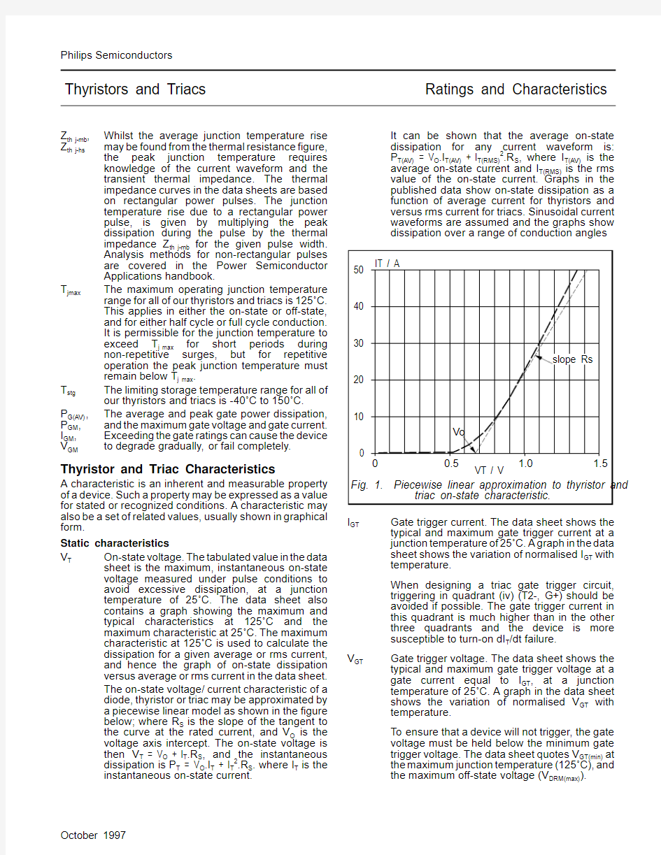
sheet is the maximum,instantaneous on-state voltage measured under pulse conditions to avoid excessive dissipation,at a junction temperature of 25?C.The data sheet also contains a graph showing the maximum and typical characteristics at 125?C and the maximum characteristic at 25?C.The maximum characteristic at 125?C is used to calculate the dissipation for a given average or rms current,and hence the graph of on-state dissipation versus average or rms current in the data sheet.The on-state voltage/current characteristic of a diode,thyristor or triac may be approximated by a piecewise linear model as shown in the figure below;where R S is the slope of the tangent to the curve at the rated current,and V O is the voltage axis intercept.The on-state voltage is then V T = V O + I T .R S ,and the instantaneous dissipation is P T = V O .I T + I T 2.R S .where I T is the instantaneous on-state current.
It can be shown that the average on-state dissipation for any current waveform is:P T(AV) = V O .I T(AV) + I T(RMS)2.R S ,where I T(AV)is the average on-state current and I T(RMS)is the rms value of the on-state current.Graphs in the published data show on-state dissipation as a function of average current for thyristors and versus rms current for triacs.Sinusoidal current waveforms are assumed and the graphs show dissipation over a range of conduction angles
I GT
Gate trigger current.The data sheet shows the typical and maximum gate trigger current at a junction temperature of 25?C.A graph in the data sheet shows the variation of normalised I GT with temperature.
When designing a triac gate trigger circuit,triggering in quadrant (iv)(T2-, G+)should be avoided if possible.The gate trigger current in this quadrant is much higher than in the other three quadrants and the device is more susceptible to turn-on dI T /dt failure.
V GT
Gate trigger voltage.The data sheet shows the typical and maximum gate trigger voltage at a gate current equal to I GT ,at a junction temperature of 25?C.A graph in the data sheet shows the variation of normalised V GT with temperature.
To ensure that a device will not trigger,the gate voltage must be held below the minimum gate trigger voltage.The data sheet quotes V GT(min)at the maximum junction temperature (125?C),and the maximum off-state voltage (V DRM(max)).
I L
Latching current.The latching current is the value of on-state current required to maintain conduction at the instant when the gate current is removed.A graph in the data sheets shows the variation of normalised I L with temperature.To trigger a thyristor or triac,a gate current greater than the maximum device gate trigger current I GT must be applied until the on-state current I T rises above the maximum latching current I L .This condition must be met at the lowest junction temperature.
I H
Holding current.The holding current is the value of on-state current required to maintain conduction once the device has fully turned on and the gate current has been removed.The on-state current must have previously exceeded the latching current I L .A graph in the data sheet shows the variation of normalised I H with temperature.
To turn off (commutate)a thyristor or triac,the load current must remain below I H for sufficient time to allow a return to the off-state.This condition must be met at the highest operating junction temperature (125?C).
I D ,I R
The maximum off-state leakage current,specified at rated V DRM(max),V RRM(max)at 125?C.
Dynamic characteristics dV D /dt
Critical rate of rise of off-state voltage.Displacement current caused by a high rate of rise of off-state voltage can induce a gate current sufficient to trigger the device.Devices with sensitive gates are particularly susceptible to dV D /dt triggering,and since gate trigger current decreases as junction temperature increases,the condition is worse when the device is hot.The data sheet figure is specified at 125?C using an exponential waveform and a maximum applied voltage of 67% V DRM(max).The dV D /dt is measured to 63%of the maximum voltage.To prevent sensitive gate devices from false triggering due to high rates of rise of off state voltage,1 k ?resistor in parallel with a 10nF capacitor may be fitted between gate and cathode (gate and terminal 1for a triac).This approach is less effective for standard gate devices.In this case,the preferred option is to fit an RC snubber between anode and cathode (T2and T1for a triac)to reduce the dV D /dt below the critical value.
t gt Gate controlled turn-on time.A typical turn on time of 2 μs is specified for all our thyristors and triacs.
t q
Circuit commutated turn-off time.A typical turn off time of 70 μs is specified for standard gate thyristors and 100μs for sensitive gate thyristors.
Triac Commutation
A triac is an AC conduction device and may be thought of as two thyristors in antiparallel,monolithically integrated onto the same silicon chip.In phase control circuits,the triac often has to be triggered into conduction part way into each half cycle.This means that at the end of each half cycle the on-state current in one direction must drop to zero and not resume in the other direction until the device is triggered again.This commutation turn-off capability is at the heart of triac power control applications.If the triac were truly two separate thyristors in antiparallel,this requirement would not present any problems.However,as the two are on the same piece of silicon there is the possibility that the unrecombined charge of one thyristor as it turns off may act as gate current to trigger the other thyristor as the voltage rises in the opposite direction.This phenomenon is called commutation failure.
There are two components of current which can act as gate current to cause commutation failure.One of these is the displacement current generated by the reapplied dV COM /dt.The other is the recombination current,which is mainly determined by the rate of fall of commutating current,dI COM /dt.Both tend to create a lateral volt drop in the cathode of the opposing thyristor which triggers the device in the opposite direction to the original current flow.
At low rates of fall of current,dI COM /dt,the amount of unrecombined charge is small and commutation failure occurs mainly because of the rate of rise of off-state voltage,dV COM /dt.This situation is worse for inductive loads where the rate of rise of voltage can be very high when commutation occurs.The conventional remedy for this type of commutation failure is to fit a snubber across the device to limit the rate of rise of off-state voltage dV COM /dt.
At high values of dI COM /dt as would occur with a rectifier-fed DC motor,the recombination current dominates and,above a critical value of dI COM /dt,the device will not commutate even at fairly low values of dV COM /dt.Under these conditions,a snubber will not prevent commutation failure,and the best option is to use a High Commutation Triac.
Three Quadrant Triacs
Philips three quadrant triacs,which include Hi-Com types,attempt to separate the two antiparallel thyristor structures to prevent the unrecombined charge from the conducting half becoming gate current in the other half.This is accomplished by lateral separation of the top and bottom emitters,more extensive emitter and peripheral shorting,and by a modified gate design which prevents triggering in quadrant (iv).
The device design,in addition to giving high immunity to commutation failure,also improves the off-state dV D /dt capability.They will commutate the full rated current up to 125?C without the aid of a snubber and will also withstand extremely high rates of rise of off-state voltage,in excess of 1000 V/μs.High commutation triacs can simplify circuit design by eliminating the need for RC snubbers.Typical applications include:
Motor starting,where the triac may be required to commutate the starting current;
Switching of DC operated relay coils or motors,where the time constant of the coil is much greater than the mains period;
Static switching,where it is required to turn the triac off whilst it is carrying an overload current.
dV COM /d Critical rate of rise of commutating voltage.For t conventional,as opposed to high commutation
triacs,the data sheet conditions specify a junction temperature of 95?C and a dI COM /dt given by 2.√2.π.f.I T(RMS),where f is the mains frequency (assumed to be 50Hz).This value is
the maximum rate of change of current which occurs at the zero crossing for a sine wave current equal to the rated rms value,I T(RMS).Graphs in the data sheet show the variation of dV COM /dt and with junction temperature with dI COM /dt as a parameter.
dI COM /dt Critical rate of change of commutating current.
High Commutation Triacs are intended for use in circuits where high values of both dI COM /dt and dV COM /dt can https://www.360docs.net/doc/f12348837.html,mutation capability is specified in terms of dI COM /dt,without a snubber and at the highest junction temperature,T jmax = 125?C.A graph in the data sheet shows the variation of dI COM /dt with junction temperature.
Operation up to 150?C
The maximum operating junction temperature,T jmax of Philips thyristors and triacs is 125?C.Operation above T jmax for long periods,particularly in the off-state,can give rise to reliability problems due to changes in characteristics which occur as a result of mobile charge in the glass passivation.
Furthermore,as a thyristor or triac gets hot,it becomes more susceptible to false gate triggering,off-state dV D /dt triggering,thermal runaway and commutation failure.However,it has become apparent that some customers have applications which require operation of thyristors and triacs at higher junction temperatures.
Recent improvements in Philips glass mesa technology backed up by extensive reliability testing has shown that,for certain applications,our thyristors and triacs can be operated reliably at junction temperatures up to 150?C.Typical applications where 150?C operation may be allowed include:-static switching of resistive loads,power switches for domestic appliances and electric heating applications where the device is mounted on a high temperature substrate.
Extending the upper operating junction temperature to 150?C depends very much on the application.For this reason we recommend that customers wishing to use our thyristors and triacs at 150?C contact the Field Applications Engineer at their Regional or National sales office.
电力电子课l练习题答案
1.电力电子器件一般工作在__开关__状态。 2.在通常情况下,电力电子器件功率损耗主要为__通态损耗__,而当器件开关频率较高时,功率损耗主要为__开关损耗__。 3.电力电子器件组成的系统,一般由__控制电路__、_驱动电路_、_主电路_三部分组成,由于电路中存在电压和电流的过冲,往往需添加_保护电路__。 4.按内部电子和空穴两种载流子参与导电的情况,电力电子器件可分为_单极型器件_、_双极型器件_、_复合型器件_三类。 5.电力二极管的工作特性可概括为_承受正向电压导通,承受反相电压截止_。 6.电力二极管的主要类型有_普通二极管_、_快恢复二极管_、_肖特基二极管_。 7.肖特基二极管的开关损耗_小于_快恢复二极管的开关损耗。 8.晶闸管的基本工作特性可概括为__正向电压门极有触发则导通、反向电压则截止__。 9.对同一晶闸管,维持电流IH与擎住电流IL在数值大小上有IL__大于__IH 。 10.晶闸管断态不重复电压UDSM与转折电压Ubo数值大小上应为,UDSM_大于__Ubo。 11.逆导晶闸管是将_二极管_与晶闸管_反并联_(如何连接)在同一管芯上的功率集成器件。的__多元集成__结构是为了便于实现门极控制关断而设计的。 的漏极伏安特性中的三个区域与GTR共发射极接法时的输出特性中的三个区域有对应关系,其中前者的截止区对应后者的_截止区_、前者的饱和区对应后者的__放大区__、前者的非饱和区对应后者的_饱和区__。 14.电力MOSFET的通态电阻具有__正__温度系数。 的开启电压UGE(th)随温度升高而_略有下降__,开关速度__小于__电力MOSFET 。16.按照驱动电路加在电力电子器件控制端和公共端之间的性质,可将电力电子器件分为_电压驱动型_和_电流驱动型_两类。 的通态压降在1/2或1/3额定电流以下区段具有__负___温度系数,在1/2或1/3额定电流以上区段具有__正___温度系数。 18.在如下器件:电力二极管(Power Diode)、晶闸管(SCR)、门极可关断晶闸管(GTO)、电力晶体管(GTR)、电力场效应管(电力MOSFET)、绝缘栅双极型晶体管(IGBT)中,属于不可控器件的是_电力二极管__,属于半控型器件的是__晶闸管_,属于全控型器件的是_GTO 、GTR 、电力MOSFET 、IGBT _;属于单极型电力电子器件的有_电力MOSFET _,属于双极型器件的有_电力二极管、晶闸管、GTO 、GTR _,属于复合型电力电子器件得有__ IGBT _;在可控的器件中,容量最大的是_晶闸管_,工作频率最高的是_电力MOSFET,属于
双向可控硅好坏检测方法
双向可控硅好坏检测方法 双向可控硅是在普通可控硅的基础上发展而成的,它不仅能代替两只反极性并联的可控硅,而且仅需一个触发电路,是比较理想的交流开关器件。其英文名称TRIAC即三端双向交流开关之意。 1.双向可控硅的检测 方法一: 测量极间电阻法。将万用表置于皮R×1k档,如果测得T2-T1、T2-G之间的正反向电阻接近∞,而万用表置于R×10档测得T1-G之间的正反向电阻在几十欧姆时,就说明双向可控硅是好的,可以使用;反之,若测得T2-T1,、T2-G之间的正反向电阻较小甚或等于零.而Tl-G之间的正反向电阻很小或接近于零时.就说明双向可控硅的性能变坏或击穿损坏。不能使用;如果测得T1-G之间的正反向电阻很大(接近∞)时,说明控制极G与主电极T1之间内部接触不良或开路损坏,也不能使用。 方法二: 检查触发导通能力。万用表置于R×10档:①如图,1(a)所示,用黑表笔接主电极T2,红表笔接T1,即给T2加正向电压,再用短路线将G与T1(或T2)短接一下后离开,如果表头指针发生了较大偏转并停留在一固定位置,说明双向可控硅中的一部分(其中一个单向可控硅)是好的,如图1(b)所示,改黑表笔接主电极T1,红表笔接T2,即给T1加正向电压,再用短路线将G与T1(或T2)短接一下后离开,如果结果同上,也证明双向可控硅中的另一部分(其中的一个单向可控硅是好的。测试到止说明双向可控硅整个都是好的,即在两个方向(在不同极性的触发电压证)均能触发导通。 图1判断双向可控硅的触发导通能力 方法三: 检查触发导通能力。如图2所示.取一只10uF左右的电解电容器,将万用表置于R×10k档(V电压),对电解电容器充电3~5s后用来代替图1中的短路线,即利用电容器上所充的电压作为触发信号,然后再将万用表置于R×10档,照图2(b)连接好后进行测试。测试时,电容C的极性可任意连接,同样是碰触
可控硅参数名词解释
晶闸管参数名词解释 1. 反向重复峰值电压(VRRM):反向阻断晶闸管两端出现的重复最大瞬时值反向电压,包括所有的重复瞬态电压,但不包括所有的不重复瞬态电压。 注:反向重复峰值电压(VRRM)是可重复的,值大于工作峰值电压的最大值电压,如每个周期开关引起的毛疵电压。 2. 反向不重复峰值电压(VRSM):反向阻断晶闸管两端出现的任何不重复最大瞬时值瞬态反向电压。 1)测试目的:在规定条件下,检验晶闸管的反向不重复峰值电压额定值。 2)测试条件:a)结温:25℃和125℃;b)门极断路;c)脉冲电压波形:底宽近似10mS 的正弦半波;d)脉冲重复频率:单次脉冲;e)脉冲次数:按有关产品标准规定;f)测试电压:反向不重复峰值电压 注:反向不重复峰值电压(VRSM)是外部因素偶然引起的,值一般大于重复峰值电压的最大值电压。通常标准规定VRSM =1.11VRRM。应用设计应考虑一切偶然因素引起的过电压都不得超过不重复峰值电压。 3. 通态方均根电流(IT(RMS)):通态电流在一个周期内的方均根值。 4. 通态平均电流(IT(AV)):通态电流在一个周期内的平均值。 5. 浪涌电流(ITSM):一种由于电路异常情况(如故障)引起的,并使结温超过额定结温的不重复性最大通态过载电流。 1)测试目的:在规定条件下,检验晶闸管的通态(不重复)浪涌电流额定值。 2)测试条件:a)浪涌前结温:125℃;b)反半周电压:80%反向重复峰值电压;d)每次浪涌的周波数:一个周波,其导通角应在160度至180度之间 6. 通态电流临界上升率(di/dt):在规定条件下,晶闸管能承受而无有害影响的最大通态电流上升率。 1)测试目的:在规定条件下,检验晶闸管的通态电流临界上升率额定值。 2)测试条件:a)加通态电流前结温:125℃;b)门极触发条件:IGM =3~5IGT;c)开通前断态电压VDM=2/3VDRM ;d)开通后通态电流峰值:2 IT(AV)~3IT(AV);e)t1≥1us;f)重复频率:50HZ;g)通态电流持续时间:5s。 7. I2t值:浪涌电流的平方在其持续时间内的积分值。 1)测试目的:在规定条件下,检验和测量反向阻断三级晶闸管的I2t值 2)测试条件:a)浪涌前结温:125℃;b)浪涌电流波形:正弦半波; 3) I2t测试实质是持续时间小于工频正弦波(1-10ms范围)的一种不重复浪涌电流测试。通过浪涌电流it对其持续时间t积分∫it2dt,即可求得I2t值。 8. 门极平均值耗散功率(PG(AV)):在规定条件下,门极正向所允许的最大平均功率。 1) 测试目的:在规定条件下,检验反向阻断三级晶闸管的门极平均功率额定值 2) 测试条件:a)结温:125℃;b)门极功率:额定门极平均功率;c)测试持续时间:3S;d)主电路条件:阳,阴极间断路。 3)测量程序:a)被测器件加热到规定结温;b)从零缓慢调整电源的输出,使电流表和电压表指示的数字的乘积达到额定门极平均功率PG(AV),并保持3S时间,然后将电源的输出调回零;c)测试后,进行门极触发电流和电压测量,如无异常,则PG(AV)额定值得到确认。 9. 反向重复峰值电流(IRRM):晶闸管加上反向重复峰值电压时的峰值电流。 10. 断态重复峰值电流(IDRM):晶闸管加上断态重复峰值电压时的峰值电流。
单向可控硅与双向可控硅的导通条件及特点
一、单向可控硅工作原理 可控硅导通条件:一是可控硅阳极与阴极间必须加正向电压,二是控制极也要加正向电压。以上两个条件必须同时具备,可控硅才会处于导通状态。另外,可控硅一旦导通后,即使降低控制极电压或去掉控制极电压,可控硅仍然导通。 可控硅关断条件:降低或去掉加在可控硅阳极至阴极之间的正向电压,使阳极电流小于最小维持电流以下。 二、单向可控硅的引脚区分 对可控硅的引脚区分,有的可从外形封装加以判别,如外壳就为阳极,阴极引线比控制极引线长。从外形无法判断的可控硅,可用万用表R×100或R×1K挡,测量可控硅任意两管脚间的正反向电阻,当万用表指示低阻值(几百欧至几千欧的范围)时,黑表笔所接的是控制极G,红表笔所接的是阴极C,余下的一只管脚为阳极A。 三、单向可控硅的性能检测 可控硅质量好坏的判别可以从四个方面进行。第一是三个PN结应完好;第二是当阴极与阳极间电压反向连接时能够阻断,不导通;第三是当控制极开路时,阳极与阴极间的电压正向连接时也不导通;第四是给控制极加上正向电流,给阴极与阳极加正向电压时,可控硅应当导通,把控制极电流去掉,仍处于导通状态。 用万用表的欧姆挡测量可控硅的极间电阻,就可对前三个方面的好坏进行判断。具体方法是:用R×1k或R×10k挡测阴极与阳极之间的正反向电阻(控制极不接电压),此两个阻值均应很大。电阻值越大,表明正反向漏电电流愈小。如果测得的阻值很低,或近于无穷大,说明可控硅已经击穿短路或已经开路,此可控硅不能使用了。 用R×1k或R×10k挡测阳极与控制极之间的电阻,正反向测量阻值均应几百千欧以上,若电阻值很小表明可控硅击穿短路。 用R×1k或R×100挡,测控制极和阴极之间的PN结的正反向电阻在几千欧左右,如出现正向阻值接近于零值或为无穷大,表明控制极与阴极之间的PN结已经损坏。反向阻值应很大,但不能为无穷大。正常情况是反向阻值明显大于正向阻值。 万用表选电阻R×1挡,将黑表笔接阳极,红表笔仍接阴极,此时万用表指针应不动。红表笔接阴极不动,黑表笔在不脱开阳极的同时用表笔尖去瞬间短接控制极,此时万用表电阻挡指针应向右偏转,阻值读数为10欧姆左右。如阳极接黑表笔,阴极接红表笔时,万用表指针发生偏转,说明该单向可控硅已击穿损坏。 四、可控硅的使用注意事项 选用可控硅的额定电压时,应参考实际工作条件下的峰值电压的大小,并留出一定的余量。 1、选用可控硅的额定电流时,除了考虑通过元件的平均电流外,还应注意正常工作时导通角的大小、散热通风条件等因素。在工作中还应注意管壳温度不超过相应电流下的允许值。 2、使用可控硅之前,应该用万用表检查可控硅是否良好。发现有短路或断路现象时,应立即
晶闸管直流调速系统参数和环节特性的测定
晶闸管直流调速系统参数和环节特性的测定一、实验目的 (1)熟悉晶闸管直流调速系统的组成及其基本结构。 (2)掌握晶闸管直流调速系统参数及反馈环节测定方法。 二、实验原理 晶闸管直流调速系统由整流变压器、晶闸管整流调速装置、平波电抗器、电动机-发动机组等组成。 在本实验中,整流装置的主电路为三相桥式电路,控制电路可直接由给定电压U g作为触发器的移相控制电压U ct,改变U g的大小即可改变控制角α,从而获得可调直流电压,以满足实验要求。实验系统的组成原理如图1所示。 图1 晶闸管直流调速试验系统原理图
三、实验内容 (1) 测定晶闸管直流调速系统主电路总电阻值R 。 (2) 测定晶闸管直流调速系统主电路电感值L 。 (3) 测定直流电动机-直流发电机-测速发电机组的飞轮惯量GD 2。 (4) 测定晶闸管直流调速系统主电路电磁时间常数T d 。 (5) 测定直流电动机电势常数C e 和转矩常数C M 。 (6) 测定晶闸管直流调速系统机电时间常数T M 。 (7) 测定晶闸管触发及整流装置特性()ct d U f U =。 (8) 测定测速发电机特性()n f U TG =。 四、实验仿真 晶体管直流调速实验系统原理图如图1所示。该系统由给定信号、同步脉冲触发器、晶闸管整流桥、平波电抗器、直流电动机等部分组成。图2是采用面向电气原理图方法构成的晶闸管直流调速系统的仿真模型。下面介绍各部分的建模与参数设置过程。 4.1 系统的建模和模型参数设置 系统的建模包括主电路的建模与控制电路的建模两部分。 (1)主电路的建模与参数设置 由图2可见,开环直流调速系统的主电路由三相对称交流电压源、晶闸管整流桥、平波电抗器、直流电动机等部分组成。由于同步脉冲触发器与晶闸管整流桥是不可分割的两个环节,通常作为一个组合体来讨论,所以将触发器归到主电路进行建模。 ①三相对称交流电压源的建模和参数设置。首先从电源模块组中选取一个交流电压源模块,再用复制的方法得到三相电源的另两个电压源模块,并用模块标题名称修改方法将模块标签分别改为“A 相”、“B 相”、“C 相”,然后从元件模块
晶闸管的结构以及工作原理
一、晶闸管的基本结构 晶闸管(SemiconductorControlled Rectifier 简称SCR )是一种四层结构(PNPN )的大功率半导体器件,它同时又被称作可控整流器或可控硅元件。它有三个引出电极,即阳极(A )、阴极(K )和门极(G )。其符号表示法和器件剖面图如图1所示。 图1 符号表示法和器件剖面图 普通晶闸管是在N 型硅片中双向扩散P 型杂质(铝或硼),形成211P N P 结构,然后在2P 的大部分区域扩散N 型杂质(磷或锑)形成阴极,同时在2P 上引出门极,在1P 区域形成欧姆接触作为阳极。 图2、晶闸管载流子分布 二、晶闸管的伏安特性 晶闸管导通与关断两个状态是由阳极电压、阳极电流和门极电流共同决定的。通常用伏安特性曲线来描述它们之间的关系,如图3所示。 图3 晶闸管的伏安特性曲线 当晶闸管AK V 加正向电压时,1J 和3J 正偏,2J 反偏,外加电压几乎全部降落在2J 结上,2J 结起到阻断电流的作用。随着AK V 的增大,只要BO AK V V <,通过阳极电流A I 都很小,因而称此区域为正向阻断状态。当AK V 增大超过BO V 以后,阳极电流突然增大,特性曲线过负阻过程瞬间变到低电压、大电流状态。晶闸管流过由负载决定的通态电流T I ,器件压降为1V 左右,特性曲线CD 段对应的状态称为导通状态。通常将BO V 及其所对应的BO I 称之为正向转折电压和转折电流。晶闸管导通后能自身维持同态,从通态转换到断态,通常是不用门极信号而是由外部电路控制,即只有当电流小到称为维持电流H I 的某一临界值以下,器件才能被关断。 当晶闸管处于断态(BO AK V V <)时,如果使得门极相对于阴极为正,给门极通以电流G I ,那么晶闸管将在较低的电压下转折导通。转折电压BO V 以及转折电流BO I 都是G I 的函数,G I 越大,BO V 越小。如图3所示,晶闸管一旦导通后,即使去除门极信号,器件仍然然导通。
可控硅(SCR)知识
可控硅(SCR)知识 可控硅(SCR)国际通用名称为Thyyistoy,中文简称晶闸管。它能在高电压、大电流条件下工作,具有耐压高、容量大、体积小等优点,它是大功率开关型半导体器件,广泛应用在电力、电子线路中。 1.可控硅的特性。可控硅分单向可控硅、双向可控硅。单向可控硅有阳极A、阴极K、控制极G 三个引出脚。双向可控硅有第一阳极A1(T1),第二阳极A2(T2)、控制极G 三个引出脚。只有当单向可控硅阳极A 与阴极K 之间加有正向电压,同时控制极 G 与阴极间加上所需的正向触发电压时,方可被触发导通。此时A、K 间呈低 阻导通状态,阳极A 与阴极K 间压降约1V。单向可控硅导通后,控制器G 即使失去触发电压,只要阳极A 和阴极K 之间仍保持正向电压,单向可控硅继 续处于低阻导通状态。只有把阳极A 电压拆除或阳极A、阴极K 间电压极性发生改变(交流过零)时,单向可控硅才由低阻导通状态转换为高阻截止状态。 单向可控硅一旦截止,即使阳极A 和阴极K 间又重新加上正向电压,仍需在 控制极G 和阴极K 间有重新加上正向触发电压方可导通。单向可控硅的导通 与截止状态相当于开关的闭合与断开状态,用它可制成无触点开关。双向可控硅第一阳极A1 与第二阳极A2 间,无论所加电压极性是正向还是反向,只 要控制极G 和第一阳极A1 间加有正负极性不同的触发电压,就可触发导通呈 低阻状态。此时A1、A2 间压降也约为1V。双向可控硅一旦导通,即使失去触发电压,也能继续保持导通状态。只有当第一阳极A1、第二阳极A2 电流减小,小于维持电流或A1、A2 间当电压极性改变且没有触发电压时,双向可控硅才 截断,此时只有重新加触发电压方可导通。 2.单向可控硅的检测。万用表选电阻R*1Ω挡,用红、黑两表笔分别测任意两引脚间正反向电阻直至找出读数 为数十欧姆的一对引脚,此时黑表笔的引脚为控制极G,红表笔的引脚为阴极
可控硅元件的工作原理及基本特性
可控硅元件的工作原理及基本特性 1、工作原理 可控硅是P1N1P2N2四层三端结构元件,共有三个PN结,分析原理时,可以把它看作由一个PNP管和一个NPN管所组成,其等效图解如图1所示 图1 可控硅等效图解图 当阳极A加上正向电压时,BG1和BG2管均处于放大状态。此时,如果从控制极G输入一个正向触发信号,BG2便有基流ib2流过,经BG2放大,其集电极电流ic2=β2ib2。因为BG2的集电极直接与BG1的基极相连,所以ib1=ic2。此时,电流ic2再经BG1放大,于是BG1的集电极电流ic1=β1ib1=β1β2ib2。这个电流又流回到BG2的基极,表成正反馈,使ib2不断增大,如此正向馈循环的结果,两个管子的电流剧增,可控硅使饱和导通。 由于BG1和BG2所构成的正反馈作用,所以一旦可控硅导通后,即使控制极G的电流消失了,可控硅仍然能够维持导通状态,由于触发信号只起触发作用,没有关断功能,所以这种可控硅是不可关断的。 由于可控硅只有导通和关断两种工作状态,所以它具有开关特性,这种特性需要一定的条件才能转化,此条件见表1 状态条件说明 从关断到导通1、阳极电位高于是阴极电位 2、控制极有足够的正向电压和电流 两者缺一不可 维持导通1、阳极电位高于阴极电位 2、阳极电流大于维持电流 两者缺一不可 从导通到关断1、阳极电位低于阴极电位 2、阳极电流小于维持电流 任一条件即可 2 可控硅的基本伏安特性见图2 图2 可控硅基本伏安特性 (1)反向特性 当控制极开路,阳极加上反向电压时(见图3),J2结正偏,但J1、J2结反偏。此时只能流过很小的反向饱和电流,当电压进一步提高到J1结的雪崩击穿电压后,接差J3结也击穿,电流迅速增加,图3的特性开始弯曲,如特性OR段所示,弯曲处的电压URO叫“反向转折电压”。此时,可控硅会发生永久性反向击穿。
可控硅的主要参数
可控硅 可控硅是硅可控整流元件的简称,亦称为晶闸管。具有体积小、结构相对简单、功能强等特点,是比较常用的半导体器件之一。该器件被广泛应用于各种电子设备和电子产品中,多用来作可控整流、逆变、变频、调压、无触点开关等。家用电器中的调光灯、调速风扇、空调机、电视机、电冰箱、洗衣机、照相机、组合音响、声光电路、定时控制器、玩具装置、无线电遥控、摄像机及工业控制等都大量使用了可控硅器件。按其工作特性,可控硅(THYRISTOR)可分为普通可控硅(SCR)即单向可控硅、双向可控硅(TRIAC)和其它特殊可控硅。 可控硅的主要参数 非过零触发-无论交流电电压在什么相位的时候都可触发导通可控硅,常见的是移相触发,即通过可控硅的主要参数 1、额定通态平均电流IT在一定条件下,阳极---阴极间可以连续通过的50赫兹正弦半波电流的平均值。 2、正向阻断峰值电压VPF 在控制极开路未加触发信号,阳极正向电压还未超过导能电压时,可以重复加在可控硅两端的正向峰值电压。可控硅承受的正向电压峰值,不能超过手册给出的这个参数值。 3、反向阴断峰值电压VPR当可控硅加反向电压,处于反向关断状态时,可以重复加在可控硅两端的反向峰值电压。使用时,不能超过手册给出的这个参数值。 4、控制极触发电流Ig1 、触发电压VGT在规定的环境温度下,阳极---阴极间加有一定电压时,可控硅从关断状态转为导通状态所需要的最小控制极电流和电压。
5、维持电流IH在规定温度下,控制极断路,维持可控硅导通所必需的最小阳极正向电流。 近年来,许多新型可控硅元件相继问世,如适于高频应用的快速可控硅,可以用正或负的触发信号控制两个方向导通的双向可控硅,可以用正触发信号使其导通,用负触发信号使其关断的可控硅等等。 可控硅的触发 过零触发-一般是调功,即当正弦交流电交流电电压相位过零点触发,必须是过零点才触发,导通可控硅。 非过零触发-无论交流电电压在什么相位的时候都可触发导通可控硅,常见的是移相触发,即通过改变正弦交流电的导通角(角相位),来改变输出百分比。 可控硅的主要参数 可控硅的主要参数: 1 额定通态电流(IT)即最大稳定工作电流,俗称电流。常用可控硅的IT一般为一安到几十安。 2 反向重复峰值电压(VRRM)或断态重复峰值电压(VDRM),俗称耐压。常用可控硅的VRRM/VDRM一般为几百伏到一千伏。 3 控制极触发电流(IGT),俗称触发电流。常用可控硅的IGT一般为几微安到几十毫安。可控硅的常用封装形式
晶闸管的结构及性能特点
晶闸管的结构及性能特点 (一)普通晶闸管 普通晶闸管(SCR)是由PNPN四层半导体材料构成的三端半导体器件,三个引出端分另为阳极A、阴极K和门极G、图8-4是其电路图形符号。 普通晶闸管的阳极与阴极之间具有单向导电的性能,其内部可以等效为由一只PNP晶闸管和一只NPN晶闸管组成的组合管,如图8-5所示。 当晶闸管反向连接(即A极接电源负端,K极接电源正端)时,无论门极G 所加电压是什么极性,晶闸管均处于阻断状态。当晶闸管正向连接(即A极接电源正端,K极接电源负端)时,若门极G所加触发电压为负时,则晶闸管也不导通,只有其门极G加上适当的正向触发电压时,晶闸管才能由阻断状态变为导通状态。此时,晶闸管阳极A极与阴极K极之间呈低阻导通状态,A、K 极之间压降约为1V。 普通晶闸管受触发导通后,其门极G即使失去触发电压,只要阳极A和阴极K 之间仍保持正向电压,晶闸管将维持低阻导通状态。只有把阳极A电压撤除或
阳极A、阴极K之间电压极性发生改变(如交流过零)时,普通晶闸管才由低阻导通状态转换为高阻阻断状态。普通晶闸管一旦阻断,即使其阳极A与阴极K 之间又重新加上正向电压,仍需在门极G和阴极K之间重新加上正向触发电压后方可导通。 普通晶闸管的导通与阻断状态相当于开关的闭合和断开状态,用它可以制成无触点电子开关,去控制直流电源电路。 (二)双向晶闸管 双向晶闸管(TRIAC)是由NPNPN五层半导体材料构成的,相当于两只普通晶闸管反相并联,它也有三个电极,分别是主电极T1、主电极T2和门极G。图8-6是双向晶闸管的结构和等效电路,图8-7是其电路图形符号。
双向晶闸管可以双向导通,即门极加上正或负的触发电压,均能触发双向晶闸管正、反两个方向导通。图8-8是其触发状态。
晶闸管的基本检测方法
晶闸管的基本检测方法 1.判别单向晶闸管的阳极、阴极和控制极 脱开电路板的单向晶闸管,阳极、阴极和控制极3个引脚一般没有特殊的标注,识别各个脚主要是通过检测各个引脚之间的正、负电阻值来进行的。晶闸管各个引脚之间的阻值都较大,当检测出现唯一一个小阻值时,此时黑表笔接的是控制极(G),红表笔接的是阴极(K),另外一个引脚就是阳极(A)。 2.判别单向晶闸管的好坏 脱开电路板的单向晶闸管,阳极(A)、阴极(K)和控制极(G)明确标示;正常的单向闸管,阳极(A)、阴极(K)两个引脚之间的正、反向电阻,阳极(A)、控制极(G)两个引脚之间的正、反向电阻的阻值应该都很大,阴极(K)、控制极(G)两个引脚之间的正向电阻应该远小于反向电阻。并且阳极(A)、阴极(K)两个引脚之间的正向电阻越大,单向晶闸管阳极的正向阻断特性越好;反向电阻越大,单向晶闸管阳极的反向阻断特性越好。 3.判别双向晶闸管的好坏 脱开电路板的双向晶闸管,第一电极(T1)、第二电极(T2)、控制极(G)明确。判断双向晶闸管的好坏,主要是看短路前第二电极(T2)和第一电极(T1)之间阻值接近无穷大,第二电极(T2)与控制极(G)引脚短路,短路后晶闸管触发导通,第二电极(T2)·和第一电极(T1)之间的电阻变小,有固定值。可以断定该双向晶闸管具备双向触发能力,性能基本良好。 4.晶闸管的代换原则 晶闸管的品种繁多,不同的电子设备与不同的电子电路,采用不同类型的晶闸管。选用与代换晶闸管时,主要应考虑其额定峰值电压、额定电流、正向压降、门极触发电流及触发电压、开关速度等参数,额定峰值电压和额定电流均应高于工作电路的最大工作电压和最大工作电流1.5~2倍,代换时最好选用同类型、同特性、同外形的晶闸管替换。 普通晶闸管一般被用于交直流电压控制、可控整流、交流调压、逆变电源,开关电源保护等电路。 双向晶闸管一般被用于交流开关、交流调压、交流电动机线性凋速、灯具线性调光及固态继电器、固态接触器等电路。 逆导晶闸管一般被用于电磁灶、电子镇流器、超声波电路、超导磁能贮存系统及开关电源等电路。 光控晶闸管一般被用于光电耀合器、光探测器、光报警器、光计数器、光电逻辑电路及自动生产线的运行监控电路等。 BTC晶体管一般被用于锯齿波发生器、长时间延时器、过电压保护器及大功率晶体管触发电路等。 门极关断晶闸管一般被用于交流电动机变频调速、斩波器、逆变电源及各种电子开关电路等。
可控硅参数列表
March 2008 Rev. 21/9 AN2703 Application note Parameter list for SCRs, TRIACs, AC switches, and DIACS Introduction All datasheet parameters are rated as minimum or maximum values, corresponding to the product parameter distribution. In each datasheet, two classes of parameters are available:■ Absolute ratings, corresponding to critical parameters, not to be exceeded for safe operation. If the absolute rating is exceeded, the component may be damaged.■Electrical, thermal and static characteristics, defining limits on product https://www.360docs.net/doc/f12348837.html,
Parameters AN2703 1 Parameters 2/9
AN2703Parameters 3/9I GM Peak gate current This is the maximum peak current allowed through gate and cathode, defined for a 20 μs pulse duration. If the absolute rating is exceeded, the component may be damaged. P G(AV)Average gate power dissipation This is the maximum average power that can be dissipated by the gate junction. If the absolute rating is exceeded, the component may be damaged. V RGM Peak reverse gate voltage This parameter is only defined for SCRs. It is the maximum reverse voltage than can be applied across gate and cathode terminals, without risk of destruction of the gate to cathode junction. V GM Peak positive gate voltage (with respect to the pin "COM") This parameter is only defined for ACSs. It is the maximum voltage than can be applied across gate and COM terminals without risk of destruction of the gate to COM junction.Table 2.Electrical characteristics parameters Parameter Name and description P Average power dissipation This is the average power dissipated by current conduction through the device for one full cycle operation. I GT Triggering gate current This is the current to apply between gate and cathode (or gate and electrode A1 for TRIAC) to turn-on the device. This parameter defines the sensitivity of the component. For a SCR, the gate current has always to be sunk by the gate. For a TRIAC, I GT is define for 3 or 4 quadrants corresponding to the different polarities of A2, A1 and gate: - Q1: I g sunk by the gate, V A2-A1 > 0 - Q2: I g sourced by the gate, V A2-A1 > 0 - Q3: I g sourced by the gate, V A2-A1 < 0 - Q4: I g sunk by the gate, V A2-A1 < 0 The I GT value is higher in Q4 quadrant. For ACS types, I GT is defined in two quadrants (Q2 and Q3). V GT Triggering gate voltage This is the voltage to apply across gate and cathode (or gate and electrode A1 for TRIAC) to reach the IGT current and then to trigger the device. V GD Non-triggering gate voltage V GD is the maximum voltage which can be applied across gate and cathode (or gate and electrode A1 for TRIAC) without causing undesired turn-on. This parameter is specified, for the worst case scenario, at the maximum junction temperature.Table 1.Absolute ratings parameters (continued) Parameter Name and description
双向可控硅的控制原理
双向可控硅的工作原理 1.可控硅是P1N1P2N2四层三端结构元件,共有三个PN结,分析原理时,可以把它看作由一个PNP管和一个NPN管所组成 当阳极A加上正向电压时,BG1和BG2管均处于放大状态。此时,如果从控制极G输入一个正向触发信号,BG2便有基流ib2流过,经BG2放大,其集电极电流ic2=β2ib2。因为BG2的集电极直接与BG1的基极相连,所以ib1=ic2。此时,电流ic2再经BG1放大,于是BG1的集电极电流ic1=β1ib1=β1β2ib2。这个电流又流回到BG2的基极,表成正反馈,使ib2不断增大,如此正向馈循环的结果,两个管子的电流剧增,可控硅使饱和导通。 由于BG1和BG2所构成的正反馈作用,所以一旦可控硅导通后,即使控制极G的电流消失了,可控硅仍然能够维持导通状态,由于触发信号只起触发作用,没有关断功能,所以这种可控硅是不可关断的。 由于可控硅只有导通和关断两种工作状态,所以它具有开关特性,这种特性需要一定的条件才能转化 2,触发导通 在控制极G上加入正向电压时(见图5)因J3正偏,P2区的空穴时入N2区,N2区的电子进入P2区,形成触发电流IGT。在可控硅的内部正反馈作用(见图2)的基础上,加上IGT的作用,使可控硅提前导通,导致图3的伏安特性OA段左移,IGT越大,特性左移越快。 一、可控硅的概念和结构? 晶闸管又叫可控硅。自从20世纪50年代问世以来已经发展成了一个大的家族,它的主要成员有单向晶闸管、双向晶闸管、光控晶闸管、逆导晶闸管、可关断晶闸管、快速晶闸管,等等。今天大家使用的是单向晶闸管,也就是人们常说的普通晶闸管,它是由四层半导体材料组成的,有三个PN结,对外有三个电极〔图2(a)〕:第一层P型半导体引出的电极叫阳极A,第三层P型半导体引出的电极叫控制极G,第四层N型半导体引出的电极叫阴极K。从晶闸管的电路符号〔图2(b)〕可以看到,它和二极管一样是一种单方向导电的器件,关键是多了一个控制极G,这就使它具有与二极管完全不同的工作特性。
单向晶闸管的基本结构及工作原理
单向晶闸管的基本结构及工作原理 晶闸管有许多种类,下面以常用的普通晶闸管为例,介绍其基本结构及工作原理。 单向晶闸管内有三个PN 结,它们是由相互交叠的4 层P区和N区所构成的.如图17-1(a) 所示。晶闸管的三个电极是从P1引出阳极A,从N2引出阳极K ,从P2引出控制极G ,因此可以说它是一个四层三端 半导体器件。 为了便于说明.可以把图17-1 (a) 所示晶闸管看成是由两部分组成的[见图17-1(b)],这样可以把晶闸管等效为两只三极管组成的一对互补管.左下部分为NPN型管,在上部分为PNP 型管[见图17-1 (c)]。 当接上电源Ea后,VT1及VT2都处于放大状态,若在G 、K 极间加入一个正触发信号,就相当于在V T1基极与发射极回路中有一个控制电流IC,它就是VT1的基极电流IB1。经放大后,VT1产生集电极电流ICI。此电流流出VT2 的基极,成为VT2 的基极电流IB2。于是, VT2 产生了集电极电流IC2。IC2再流入VT1 的基极,再次得到放大。这样依次循环下去,一瞬间便可使VT1和VT2全部导通并达到饱和。所以,当晶闸管加上正电压后,一输入触发信号,它就会立即导通。晶闸管一经导通后,由于导致VT1基极上总是流过比控制极电流IG大得多的电流,所以即使触发信号消失后,晶闸管仍旧能保持导通状态。只有降低电源电压Ea,使VT1、VT2 集电极电流小于某一维持导通的 最小值,晶闸管才能转为关断状态。 如果把电源Ea反接,VT1 和VT2 都不具备放大工作条件,即使有触发信号,晶闸管也无法工作而处于关断状态。同样,在没有输入触发信号或触发信号极性相反时,即使晶闸管加上正向电压.它也无法导通。 上述的几种情况可参见图17-2 。
可控硅的应用参数
图1b电路为MOC3061的典型功率扩展电路,在控制功率较大的电机时,应考虑使用功率扩展电路。制作时,可参考图示参数选择器件。由于电源采用电容压降方式,请自制时注意安全,人体不能直接触摸电路板。 电路见图1a。电路中NE555接成占空比可调的方波发生器,调节RW可改变占空比。在NE555的3脚输出高电平期间,过零通断型光电耦合器MOC3061初级得到约10mA正向工作电流,使内部硅化镓红外线发射二极管发射红外光,将过零检测器中光敏双向开关于市电过零时导通,接通电风扇电机电源,风扇运转送风。在NE555的3脚输出低电平期间,双向开关关断,风扇停转。 MOC3061本身具有一定驱动能力,可不加功率驱动元件而直接利用 MOC3061的内部双向开关来控制电风扇电机的运转。RW为占空比调节电位器,
RC电路用来降低DV/DT防止误触发 MOC3061参数:技术文档数据: 触发电流在Ift=15mA到maxIf=60mA之间。 Led触发电流:Ift=15mA, A ll d evices a re gu a r a ntee d to trigger a t a n I F v a lue less th a n or equ a l to m ax I FT.Therefore,recommen d e d oper a ting I F lies b et w een m ax I FT(15m A for MOC3061-M, 10m A for MOC3062-M&MOC3162-M,5m A for MOC3063-M&MOC3163-M)a n d ab solute m ax I F(60m A). D v/D t=Pe a k B locking Current 保持通态的最小电流:IH=500u A,MT1-MT2volt a ge ab ove w hich d evice w ill not trigger 抑制电压:VINH=12(T Y P)-20(M AX)MT1-MT2VOLT A GE AB OVE W HICH D EVICE W ILL NOT TRIGGER 通态重复峰值电压V D RM=600v D V/D T=600V/US(MIN),1500(T Y P). The39ohm resistor a n d0.01μF c a p a citor a re for snu bb ing of the tri a c a n d is often,b ut not a l way s, necess a r y d epen d ing upon the p a rticul a r tri a c a n d lo ad use d. Suggeste d metho d of firing t w o,ba ck-to-ba ck SCR’s B T A16-800B:负载电流IT=16A. 维持通态电流:IH=50m A 断态电压临界上升率:D v/D t=250v/us Igt=50m A, V D RM,VRRM=800V Vgt=1.5v
晶闸管的主要参数
晶闸管的主要参数 (1) 断态不重复峰值电压U DSM 门极开路时,施加于晶闸管的阳极电压上升到正向伏安特性曲线急剧转折处所对应的电压值UDSM 。 它是一个不能重复,且每次持续时间不大于10ms的断态最大脉冲电压。UDSM值应小于转折电压U b0。 (2) 断态重复峰值电压U DRM 晶闸管在门极开路而结温为额定值时,允许重复加于晶闸管上的正向断态最大脉冲电压。 每秒50次每次持续时间不大于10ms, 规定U DRM为U DSM的90%。 (3) 反向不重复峰值电压U RSM 门极开路,晶闸管承受反向电压时,对应于反向伏安特性曲线急剧转折处的反向峰值电压值U RSM。 它是一个不能重复施加且持续时间不大于10ms的反向脉冲电压。反向不重复峰值电压U RSM 应小于反向击穿电压。 (4) 反向重复峰值电压U RRM 晶闸管在门极开路而结温为额定值时,允许重复加于晶闸管上的反向最大脉冲电压。 每秒50次每次持续时间不大于10ms。 规定U RRM为U RSM的90%。 (5) 额定电压UR 断态重复峰值电压UDRM和反向重复峰值电压URRM两者中较小的一个电压值规定为额定电压U R。 在选用晶闸管时,应该使其额定电压为正常工作电压峰值U M的2~3倍,以作为安全裕量。 (6)通态峰值电压U TM 规定为额定电流时的管子导通的管压降峰值。 一般为1.5~2.5V,且随阳极电流的增加而略为增加。 额定电流时的通态平均电压降一般为1V左右。 (7) 通态平均电流I T(AV)
在环境温度为+40℃和规定的散热冷却条件下,晶闸管在导通角不小于170°电阻性负载的单相、工频正弦半波导电,结温稳定在额定值125°时,所允许通过的最大电流平均值。 ——允许流过的最大工频正弦半波电流的平均值。 选用一个晶闸管时,要根据所通过的具体电流波形来计算出容许使用的电流有效值,该值要小于晶闸管额定电流对应的有效值。晶闸管才不会损坏。 设单相工频正弦半波电流峰值为Im 时通态平均电流为: 正弦半波电流有效值为: 有效值与通态平均电流比值为: 则有效值为: 根据有效值相等原则来计算晶闸管的额定电流。 若电路中实际流过晶闸管的电流有效值为I ,平均值I d , 定义 波形系数: 则 由于晶闸管的热容量小,过载能力低,因此在实际选择时,一般取1.5~2倍的安全系数, (8) 维持电流I H (针对关断过程) ——是指晶闸管维持导通所必需的最小电流。一般为几十到几百毫安。维持电流与结温有关,结温越高,维持电流越小,晶闸管越难关断。 (9) 断态电压临界上升率du/dt ——电压上升率过大,就会使晶闸管误导通。 ——指在额定结温和门极开路的情况下,不导致晶闸管从断态到通态转换的外加电压最大上升率。 (10) 通态电流临界上升率di/dt ——如果电流上升太快,可能造成局部过热而使晶闸管损坏 如有侵权请联系告知删除,感谢你们的配合! m T(AV)m 0I 1I I sin td(t)2πωωππ == ?m I 2I ==T(AV) I 1.57 I 2π= =T(AV)1.57I I =f d I K I =T(AV)T(AV)I 1.57I 1.57I f d K I ≤?≤T(AV)T(AV)1.57I (1.5~2.0) 1.57I (1.5~2.0) f d d f K I I K ≤?≤
可控硅的工作原理(带图)
可控硅的工作原理(带图)
可控硅的工作原理(带图) 一.可控硅是可控硅整流器的简称。它是由三个PN结四层结构硅芯片和三个电极组成的半导体器件。图3-29是它的结构、外形和图形符号。 可控硅的三个电极分别叫阳极(A)、阴极(K)和控制极(G)。当器件的阳极接负电位(相对阴极而言)时,从符号图上可以看出PN结处于反向,具有类似二极管的反向特性。当器件的阳极上加正电位时(若控制极不接任何电压),在一定的电压范围内,器件仍处于阻抗很高的关闭状态。但当正电压大于某个电压(称为转折电压)时,器件迅速转变到低阻通导状态。加在可控硅阳极和阴极间的电压低于转折电压时,器件处于关闭状态。此时如果在控制极上加有适当大小的正电压(对阴极),则可控硅可迅速被激发而变为导通状态。可控硅一旦导通,控制极便失去其控制作用。就是说,导通后撤去栅极电压可控硅仍导通,只有使器件中的电流减到低于某个数值或阴极与阳极之间电压减小到零或负值时,器件才可恢复到关闭状态。 图3-30是可控硅的伏安特性曲线。 图中曲线I为正向阻断特性。无控制极信号时,可控硅正向导通电压为正向转折电压(U B0);当有控制极信号时,正向转折电压会下降(即可以在较低正向电压下导通),转折电压随控制极电流的增大而减小。当控制极电流大到一定程度时,就不再出现正向阻断状态了。 曲线Ⅱ为导通工作特性。可控硅导通后内阻很小,管子本身压降很低,外加电压几乎全部降在外电路负载上,并流过比较大的负载电流,特性曲线与二极管正向导通特性相似。若阳极电压减小(或负载电阻增加),致使阳极电流小于维持电流I H时,可控硅从导通状态立即转为正向阻断状态,回到曲线I状态。 曲线Ⅲ为反向阻断特性。当器件的阳极加以反向电压时,尽管电压较高,但可控硅不会导通(只有很小的漏电流)。只有反向电压达到击穿电压时,电流才突然增大,若不加限制器件就会烧毁。正常工作时,外加电压要小于反向击穿电压才能保证器件安全可靠地工作。 可控硅的重要特点是:只要控制极中通以几毫安至几十毫安的电流就可以触发器件导通,器件中就可以通过较大的电流。利用这种特性可用于整流、开关、变频、交直流变换、电机调速、调温、调光及其它自动控制电路中。