KSZ9031RNX datasheet
KSZ9031RNX
Gigabit Ethernet Transceiver
with RGMII Support
Data Sheet Rev. 1.0
LinkMD is a registered trademark of Micrel, Inc.
General Description
The KSZ9031RNX is a completely integrated triple-speed (10Base-T/100Base-TX/1000Base-T) Ethernet physical-layer transceiver for transmission and reception of data on standard CAT-5 unshielded twisted pair (UTP) cable.
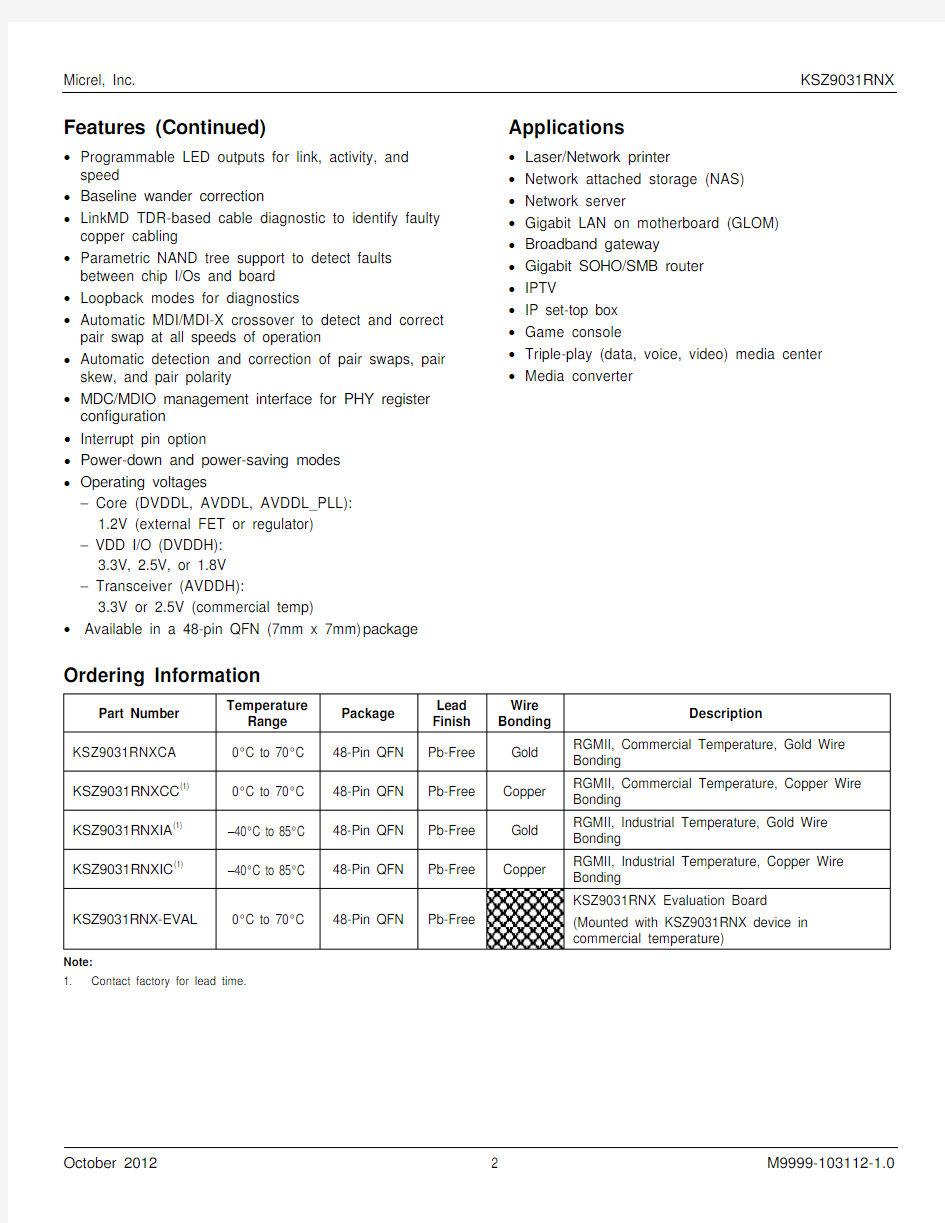
The KSZ9031RNX provides the Reduced Gigabit Media Independent Interface (RGMII) for direct connection to RGMII MACs in Gigabit Ethernet processors and switches for data transfer at 10/100/1000Mbps.
The KSZ9031RNX reduces board cost and simplifies board layout by using on-chip termination resistors for the four differential pairs and by integrating an LDO controller to drive a low-cost MOSFET to supply the 1.2V core.
The KSZ9031RNX offers diagnostic features to facilitate system bring-up and debugging in production testing and in product deployment. Parametric NAND tree support enables fault detection between KSZ9031 I/Os and the
board. The LinkMD ?
TDR-based cable diagnostic identifies faulty copper cabling. Remote and local loopback functions verify analog and digital data paths.
The KSZ9031RNX is available in a 48-pin, lead-free QFN package (see “Ordering Information”).
Data sheets and support documentation are available on Micrel’s web site at: https://www.360docs.net/doc/0716647242.html, .
Features
? Single-chip 10/100/1000Mbps IEEE 802.3 compliant Ethernet transceiver
? RGMII timing supports on-chip delay according to RGMII Version 2.0, with programming options for
external delay and making adjustments and corrections to TX and RX timing paths
? RGMII with 3.3V/2.5V/1.8V tolerant I/Os
? Auto-negotiation to automatically select the highest link-up speed (10/100/1000Mbps) and duplex (half/full) ? On-chip termination resistors for the differential pairs ? On-chip LDO controller to support single 3.3V supply operation – requires only one external FET to generate 1.2V for the core
? Jumbo frame support up to 16KB
? 125MHz reference clock output
? Energy detect power-down mode for reduced power consumption when the cable is not attached
? Energy Efficient Ethernet (EEE) support with low-power idle (LPI) mode and clock stoppage for 100Base-TX/ 1000Base-T and transmit amplitude reduction with 10Base-Te option
? Wake-on-LAN (WOL) support with robust custom-packet detection
Functional Diagram
Features (Continued)
?Programmable LED outputs for link, activity, and speed
?Baseline wander correction
?LinkMD TDR-based cable diagnostic to identify faulty copper cabling
?Parametric NAND tree support to detect faults between chip I/Os and board
?Loopback modes for diagnostics
?Automatic MDI/MDI-X crossover to detect and correct pair swap at all speeds of operation
?Automatic detection and correction of pair swaps, pair skew, and pair polarity
?MDC/MDIO management interface for PHY register configuration
?Interrupt pin option
?Power-down and power-saving modes
?Operating voltages
– Core (DVDDL, AVDDL, AVDDL_PLL):
1.2V (external FET or regulator)
– VDD I/O (DVDDH):
3.3V, 2.5V, or 1.8V
– Transceiver (AVDDH):
3.3V or 2.5V (commercial temp)
?Available in a 48-pin QFN (7mm x 7mm)package Applications
?Laser/Network printer
?Network attached storage (NAS) ?Network server
?Gigabit LAN on motherboard (GLOM) ?Broadband gateway
?Gigabit SOHO/SMB router
?IPTV
?IP set-top box
?Game console
?Triple-play (data, voice, video) media center ?Media converter
Ordering Information
Note:
1. Contact factory for lead time.
Revision History
Revision Date Summary of Changes 1.0 10/31/12 Data sheet created
Contents
General Description (1)
Features (1)
Functional Diagram (1)
Features (Continued) (2)
Applications (2)
Ordering Information (2)
Revision History (3)
Contents (4)
List of Figures (7)
List of Tables (8)
Pin Configuration (9)
Pin Description (10)
Strapping Options (15)
Functional Overview (16)
Functional Description: 10Base-T/100Base-TX Transceiver (17)
100Base-TX Transmit (17)
100Base-TX Receive (17)
Scrambler/De-Scrambler (100Base-TX only) (17)
10Base-T Transmit (17)
10Base-T Receive (17)
Functional Description: 1000Base-T Transceiver (18)
Analog Echo-Cancellation Circuit (18)
Automatic Gain Control (AGC) (18)
Analog-to-Digital Converter (ADC) (19)
Timing Recovery Circuit (19)
Adaptive Equalizer (19)
Trellis Encoder and Decoder (19)
Functional Description: 10/100/1000 Transceiver Features (19)
Auto MDI/MDI-X (19)
Pair-Swap, Alignment, and Polarity Check (20)
Wave Shaping, Slew-Rate Control, and Partial Response (20)
PLL Clock Synthesizer (20)
Auto-Negotiation (20)
RGMII Interface (22)
RGMII Signal Definition (23)
RGMII Signal Diagram (23)
RGMII Pad Skew Registers (23)
RGMII In-Band Status (27)
MII Management (MIIM) Interface (27)
Interrupt (INT_N) (28)
Single-LED Mode (28)
Tri-color Dual-LED Mode (28)
Loopback Mode (29)
Local (Digital) Loopback (29)
Remote (Analog) Loopback (30)
LinkMD? Cable Diagnostic (31)
NAND Tree Support (31)
Power Management (32)
Energy-Detect Power-Down Mode (32)
Software Power-Down Mode (32)
Chip Power-Down Mode (32)
Energy Efficient Ethernet (EEE) (32)
Transmit Direction Control (MAC-to-PHY) (33)
Receive Direction Control (PHY-to-MAC) (34)
Registers Associated with EEE (36)
Wake-On-LAN (36)
Magic-Packet Detection (36)
Customized-Packet Detection (36)
Link Status Change Detection (37)
Typical Current/Power Consumption (38)
Transceiver (3.3V), Digital I/Os (3.3V) (38)
Transceiver (3.3V), Digital I/Os (1.8V) (38)
Transceiver (2.5V), Digital I/Os (2.5V) (39)
Transceiver (2.5V), Digital I/Os (1.8V) (39)
Register Map (40)
Standard Registers (42)
IEEE Defined Registers – Descriptions (42)
Vendor-Specific Registers – Descriptions (48)
MMD Registers (52)
MMD Registers – Descriptions (53)
Absolute Maximum Ratings(1) (62)
Operating Ratings(2) (62)
Electrical Characteristics(3) (62)
Timing Diagrams (65)
RGMII Timing (65)
Auto-Negotiation Timing (66)
MDC/MDIO Timing (67)
Power-Up/Power-Down/Reset Timing (68)
Reset Circuit (69)
Reference Circuits – LED Strap-In Pins (70)
Reference Clock – Connection and Selection (71)
Magnetic – Connection and Selection (72)
Package Information (75)
Figure 1. KSZ9031RNX Block Diagram (16)
Figure 2. KSZ9031RNX 1000Base-T Transceiver Block Diagram – Single Channel (18)
Figure 3. Auto-Negotiation Flow Chart (21)
Figure 4. KSZ9031RNX RGMII Interface (23)
Figure 5. Local (Digital) Loopback (29)
Figure 6. Remote (Analog) Loopback (30)
Figure 7. LPI Mode (Refresh Transmissions and Quiet Periods) (33)
Figure 8. LPI Transition – RGMII (1000Mbps) Transmit (33)
Figure 9. LPI Transition – RGMII (100Mbps) Transmit (34)
Figure 10. LPI Transition – RGMII (1000Mbps) Receive (35)
Figure 11. LPI Transition – RGMII (100Mbps) Receive (35)
Figure 12. RGMII v2.0 Specification (Figure 3 – Multiplexing and Timing Diagram) (65)
Figure 13. Auto-Negotiation Fast Link Pulse (FLP) Timing (66)
Figure 14. MDC/MDIO Timing (67)
Figure 15. Power-Up/Power-Down/Reset Timing (68)
Figure 16. Recommended Reset Circuit (69)
Figure 17. Recommended Reset Circuit for Interfacing with CPU/FPGA Reset Output (69)
Figure 18. Reference Circuits for LED Strapping Pins (70)
Figure 19. 25MHz Crystal/Oscillator Reference Clock Connection (71)
Figure 20. Typical Gigabit Magnetic Interface Circuit (72)
Figure 21. Recommended Land Pattern, 48-Pin (7mm x 7mm) QFN (74)
Table 1. MDI/MDI-X Pin Mapping (19)
Table 2. Auto-Negotiation Timers (22)
Table 3. RGMII Signal Definition (23)
Table 4. RGMII Pad Skew Registers (24)
Table 5. Absolute Delay for 5-bit Pad Skew Setting (25)
Table 6. Absolute Delay for 4-bit Pad Skew Setting (26)
Table 7. RGMII In-Band Status (27)
Table 8. MII Management Frame Format for the KSZ9031RNX (27)
Table 9. Single-LED Mode – Pin Definition (28)
Table 10. Tri-color Dual-LED Mode – Pin Definition (28)
Table 11. NAND Tree Test Pin Order for KSZ9031RNX (31)
Table 12. Typical Current/Power Consumption – Transceiver (3.3V), Digital I/Os (3.3V) (38)
Table 13. Typical Current/Power Consumption – Transceiver (3.3V), Digital I/Os (1.8V) (38)
Table 14. Typical Current/Power Consumption – Transceiver (2.5V), Digital I/Os (2.5V) (39)
Table 15. Typical Current/Power Consumption – Transceiver (2.5V), Digital I/Os (1.8V) (39)
Table 16. Standard Registers Supported by KSZ9031RNX (40)
Table 17. MMD Registers Supported by KSZ9031RNX (41)
Table 18. Portal Registers (Access to Indirect MMD Registers) (52)
Table 19. RGMII v2.0 Specification (Timing Specifics from Table 2) (65)
Table 20. Auto-Negotiation Fast Link Pulse (FLP) Timing Parameters (66)
Table 21. MDC/MDIO Timing Parameters (67)
Table 22. Power-Up/Power-Down/Reset Timing Parameters (68)
Table 23. Reference Crystal/Clock Selection Criteria (71)
Table 24. Magnetics Selection Criteria (73)
Table 25. Compatible Single-Port 10/100/1000 Magnetics (73)
(Top View)
Pin Number Pin Name Type(1)Pin Function
1 AVDDH P 3.3V/2.5V (commercial temp only) analog V DD
2 TXRXP_A I/O Media Dependent Interface[0], positive signal of differential pair
1000Base-T mode:
TXRXP_A corresponds to BI_DA+ for MDI configuration and BI_DB+ for
MDI-X configuration, respectively.
10Base-T/100Base-TX mode:
TXRXP_A is the positive transmit signal (TX+) for MDI configuration and
the positive receive signal (RX+) for MDI-X configuration, respectively.
3 TXRXM_A I/O Media Dependent Interface[0], negative signal of differential pair
1000Base-T mode:
TXRXM_A corresponds to BI_DA– for MDI configuration and BI_DB– for
MDI-X configuration, respectively.
10Base-T/100Base-TX mode:
TXRXM_A is the negative transmit signal (TX–) for MDI configuration and
the negative receive signal (RX–) for MDI-X configuration, respectively.
4 AVDDL P 1.2V analog V DD
5 TXRXP_B I/O Media Dependent Interface[1], positive signal of differential pair
1000Base-T mode:
TXRXP_B corresponds to BI_DB+ for MDI configuration and BI_DA+ for
MDI-X configuration, respectively.
10Base-T/100Base-TX mode:
TXRXP_B is the positive receive signal (RX+) for MDI configuration and
the positive transmit signal (TX+) for MDI-X configuration, respectively.
6 TXRXM_B I/O Media Dependent Interface[1], negative signal of differential pair
1000Base-T mode:
TXRXM_B corresponds to BI_DB– for MDI configuration and BI_DA– for
MDI-X configuration, respectively.
10Base-T/100Base-TX mode:
TXRXM_B is the negative receive signal (RX–) for MDI configuration and
the negative transmit signal (TX–) for MDI-X configuration, respectively.
7 TXRXP_C I/O Media Dependent Interface[2], positive signal of differential pair
1000Base-T mode:
TXRXP_C corresponds to BI_DC+ for MDI configuration and BI_DD+ for
MDI-X configuration, respectively.
10Base-T/100Base-TX mode:
TXRXP_C is not used.
8 TXRXM_C I/O Media Dependent Interface[2], negative signal of differential pair
1000Base-T mode:
TXRXM_C corresponds to BI_DC– for MDI configuration and BI_DD– for
MDI-X configuration, respectively.
10Base-T/100Base-TX mode:
TXRXM_C is not used.
9 AVDDL P 1.2V analog V DD
10 TXRXP_D I/O Media Dependent Interface[3], positive signal of differential pair
1000Base-T mode:
TXRXP_D corresponds to BI_DD+ for MDI configuration and BI_DC+ for
MDI-X configuration, respectively.
10Base-T/100Base-TX mode:
TXRXP_D is not used.
11 TXRXM_D I/O Media Dependent Interface[3], negative signal of differential pair
1000Base-T mode:
TXRXM_D corresponds to BI_DD– for MDI configuration and BI_DC– for
MDI-X configuration, respectively.
10Base-T/100Base-TX mode:
TXRXM_D is not used.
12 AVDDH P 3.3V/2.5V (commercial temp only) analog V DD
13 NC – No connect
This pin is not bonded and can be connected to digital ground for
footprint compatibility with the Micrel KSZ9021RN Gigabit PHY.
14 DVDDL P 1.2V digital V DD
15 LED2/
PHYAD1 I/O LED output: Programmable LED2 output
Config mode: The pull-up/pull-down value is latched as PHYAD[1] during
power-up/reset. See the “Strapping Options” section for details.
The LED2 pin is programmed by the LED_MODE strapping option (pin 41), and is defined as follows:
Single-LED Mode
Link Pin State LED Definition
Link off H OFF
Link on (any speed) L ON
Tri-Color Dual-LED Mode
Link/Activity
Pin State LED Definition
LED2 LED1 LED2 LED1 Link off H H OFF OFF
1000 Link / No activity L H ON OFF
1000 Link / Activity (RX, TX) Toggle H Blinking OFF
100 Link / No activity H L OFF ON
100 Link / Activity (RX, TX) H Toggle OFF Blinking
10 Link / No activity L L ON ON
10 Link / Activity (RX, TX) Toggle Toggle Blinking Blinking
For tri-color dual-LED mode, LED2 works in conjunction with LED1 (pin 17) to
indicate 10Mbps link and activity.
16 DVDDH P 3.3V, 2.5V, or 1.8V digital V DD_I/O
17 LED1/
PHYAD0/
PME_N1 I/O LED1 output: Programmable LED1 output
Config mode: The voltage on this pin is sampled and latched during the power-
up/reset process to determine the value of PHYAD[0]. See the
“Strapping Options” section for details.
PME_N output: Programmable PME_N output (pin option 1). This pin function
requires an external pull-up resistor to DVDDH (digital V DD_I/O)
in a range from 1.0kΩ to 4.7kΩ. When asserted low, this pin
signals that a WOL event has occurred.
The LED1 pin is programmed by the LED_MODE strapping option (pin 41), and is defined as follows.
Single-LED Mode
Activity Pin State LED Definition
No activity H OFF
Activity (RX, TX) Toggle Blinking
Tri-Color Dual-LED Mode
Link/Activity
Pin State LED Definition
LED2 LED1 LED2 LED1 Link off H H OFF OFF
1000 Link / No activity L H ON OFF
1000 Link / Activity (RX, TX) Toggle H Blinking OFF
100 Link / No activity H L OFF ON
100 Link / Activity (RX, TX) H Toggle OFF Blinking
10 Link / No activity L L ON ON
10 Link / Activity (RX, TX) Toggle Toggle Blinking Blinking
For tri-color dual-LED mode, LED1 works in conjunction with LED2 (pin 15) to
indicate 10Mbps link and activity.
18 DVDDL P 1.2V digital V DD
19 TXD0 I RGMII mode: RGMII TD0 (Transmit Data 0) input
20 TXD1 I RGMII mode: RGMII TD1 (Transmit Data 1) input\
21 TXD2 I RGMII mode: RGMII TD2 (Transmit Data 2) input
22 TXD3 I RGMII mode: RGMII TD3 (Transmit Data 3) input
23 DVDDL P 1.2V digital V DD
24 GTX_CLK I RGMII mode: RGMII TXC (Transmit Reference Clock) input
25 TX_EN I RGMII mode: RGMII TX_CTL (Transmit Control) input
26 DVDDL P 1.2V digital V DD
27 RXD3/
MODE3 I/O RGMII mode: RGMII RD3 (Receive Data 3) output
Config mode: The pull-up/pull-down value is latched as MODE3 during
power-up/reset. See the “Strapping Options” section for details.
28 RXD2/
MODE2 I/O RGMII mode: RGMII RD2 (Receive Data 2) output
Config mode: The pull-up/pull-down value is latched as MODE2 during
power-up/reset. See the “Strapping Options” section for details.
29 VSS Gnd Digital ground
30 DVDDL P 1.2V digital V DD
31 RXD1/
MODE1 I/O RGMII mode: RGMII RD1 (Receive Data 1) output
Config mode: The pull-up/pull-down value is latched as MODE1 during
power-up/reset. See the “Strapping Options” section for details.
32 RXD0/
MODE0 I/O RGMII mode: RGMII RD0 (Receive Data 0) output
Config mode: The pull-up/pull-down value is latched as MODE0 during
power-up/reset. See the “Strapping Options” section for details.
33 RX_DV/
CLK125_EN I/O RGMII mode: RGMII RX_CTL (Receive Control) output
Config mode: Latched as CLK125_NDO Output Enable during
power-up/reset. See the “Strapping Options” section for details.
34 DVDDH P 3.3V, 2.5V, or 1.8V digital V DD_I/O
35 RX_CLK/
PHYAD2 I/O RGMII mode: RGMII RXC (Receive Reference Clock) output
Config mode: The pull-up/pull-down value is latched as PHYAD[2] during
power-up/reset. See the “Strapping Options” section for details.
36 MDC Ipu Management data clock input
This pin is the input reference clock for MDIO (pin 37).
37 MDIO Ipu/O Management data input/output
This pin is synchronous to MDC (pin 36) and requires an external pull-up resistor
to DVDDH (digital V DD_I/O) in a range from 1.0kΩ to 4.7kΩ.
38 INT_N/
PME_N2 O Interrupt output: Programmable interrupt output, with register 1Bh as the Interrupt
Control/Status register, for programming the interrupt conditions
and reading the interrupt status. Register 1Fh, bit [14] sets
the interrupt output to active low (default) or active high.
PME_N output: Programmable PME_N output (pin option 2). When asserted
low, this pin signals that a WOL event has occurred.
For Interrupt (when active low) and PME functions, this pin requires an external
pull-up resistor to DVDDH (digital V DD_I/O)in a range from 1.0kΩ to 4.7kΩ.
39 DVDDL P 1.2V digital V DD
40 DVDDH P 3.3V, 2.5V, or 1.8V digital V DD_I/O
41 CLK125_NDO/
LED_MODE I/O 125MHz clock output
This pin provides a 125MHz reference clock output option for use by the MAC.
Config mode: The pull-up/pull-down value is latched as LED_MODE during
power-up/reset. See the “Strapping Options” section for details.
42 RESET_N Ipu Chip reset (active low)
Hardware pin configurations are strapped-in at the de-assertion (rising edge) of
RESET_N. See the “Strapping Options” section for more details.
43 LDO_O O On-chip 1.2V LDO controller output
This pin drives the input gate of a P-channel MOSFET to generate 1.2V for the
chip’s core voltages. If the system provides 1.2V and this pin is not used, it can be
left floating.
44 AVDDL_PLL P 1.2V analog V DD for PLL
45 XO O 25MHz crystal feedback
This pin is a no connect if an oscillator or external clock source is used.
46 XI I Crystal / Oscillator/ External Clock input
25MHz ±50ppm tolerance
47 NC – No connect
This pin is not bonded and can be connected to AVDDH power for footprint
compatibility with the Micrel KSZ9021RN Gigabit PHY.
48 ISET I/O Set the transmit output level
Connect a 12.1kΩ 1% resistor to ground on this pin.
PADDLE P_GND Gnd Exposed paddle on bottom of chip
Connect P_GND to ground.
Note:
1. P = Power supply.
Gnd = Ground.
I = Input.
O = Output.
I/O = Bi-directional.
Ipu = Input with internal pull-up (see “Electrical Characteristics” for value).
Ipu/O = Input with internal pull-up (see “Electrical Characteristics” for value)/Output.
Strapping Options
Pin Number Pin Name Type(1)Pin Function
35 15 17 PHYAD2
PHYAD1
PHYAD0
I/O
I/O
I/O
The PHY address, PHYAD[2:0], is sampled and latched at power-up/reset and is
configurable to any value from 0 to 7. Each PHY address bit is configured as follows:
Pull-up = 1
Pull-down = 0
PHY address bits [4:3] are always set to ‘00’.
27
28
31
32 MODE3
MODE2
MODE1
MODE0
I/O
I/O
I/O
I/O
The MODE[3:0] strap-in pins are sampled and latched at power-up/reset as follows:
MODE[3:0] Mode
0000 Reserved – not used
0001 Reserved – not used
0010 Reserved – not used
0011 Reserved – not used
0100 NAND tree mode
0101 Reserved – not used
0110 Reserved – not used
0111 Chip power-down mode
1000 Reserved – not used
1001 Reserved – not used
1010 Reserved – not used
1011 Reserved – not used
1100 RGMII mode – advertise 1000Base-T full-duplex only
1101 RGMII mode – advertise 1000Base-T full- and half-duplex only
1110 RGMII mode – advertise all capabilities (10/100/1000 speed
half-/full-duplex), except 1000Base-T half-duplex
1111 RGMII mode – advertise all capabilities (10/100/1000 speed
half-/full-duplex)
33 CLK125_EN I/O CLK125_EN is sampled and latched at power-up/reset and is defined as follows:
Pull-up = Enable 125MHz clock output
Pull-down = Disable 125MHz clock output
Pin 41 (CLK125_NDO) provides the 125MHz reference clock output option for use by
the MAC.
41 LED_MODE I/O LED_MODE is latched at power-up/reset and is defined as follows:
Pull-up = Single-LED mode
Pull-down = Tri-color dual-LED mode
Note:
1. I/O = Bi-directional.
Pin strap-ins are latched during power-up or reset. In some systems, the MAC receive input pins may be driven during power-up or reset, and consequently cause the PHY strap-in pins on the RGMII signals to be latched to an incorrect configuration. In this case, Micrel recommends adding external pull-ups/pull-downs on the PHY strap-in pins to ensure the PHY is configured to the correct pin strap-in mode.
Functional Overview
The KSZ9031RNX is a completely integrated triple-speed (10Base-T/100Base-TX/1000Base-T) Ethernet physical layer transceiver solution for transmission and reception of data over a standard CAT-5 unshielded twisted pair (UTP) cable. Its on-chip proprietary 1000Base-T transceiver and Manchester/MLT-3 signaling-based 10Base-T/100Base-TX transceivers are all IEEE 802.3 compliant.
The KSZ9031RNX reduces board cost and simplifies board layout by using on-chip termination resistors for the four differential pairs and by integrating an LDO controller to drive a low-cost MOSFET to supply the 1.2V core.
On the copper media interface, the KSZ9031RNX can automatically detect and correct for differential pair misplacements and polarity reversals, and correct propagation delays and re-sync timing between the four differential pairs, as specified in the IEEE 802.3 standard for 1000Base-T operation.
The KSZ9031RNX provides the RGMII interface for direct and seamless connection to RGMII MACs in Gigabit Ethernet processors and switches for data transfer at 10/100/1000Mbps.
Figure 1 shows a high-level block diagram of the KSZ9031RNX.
Figure 1. KSZ9031RNX Block Diagram
Functional Description: 10Base-T/100Base-TX Transceiver
100Base-TX Transmit
The 100Base-TX transmit function performs parallel-to-serial conversion, 4B/5B coding, scrambling, NRZ-to-NRZI conversion, and MLT-3 encoding and transmission.
The circuitry starts with a parallel-to-serial conversion, which converts the RGMII data from the MAC into a 125MHz serial bit stream. The data and control stream is then converted into 4B/5B coding, followed by a scrambler. The serialized data is further converted from NRZ-to-NRZI format then transmitted in MLT-3 current output. The output current is set by an external 12.1kΩ 1% resistor for the 1:1 transformer ratio.
The output signal has a typical rise/fall time of 4ns and complies with the ANSI TP-PMD standard regarding amplitude balance, overshoot, and timing jitter. The wave-shaped 10Base-T output is also incorporated into the 100Base-TX transmitter.
100Base-TX Receive
The 100BASE-TX receiver function performs adaptive equalization, DC restoration, MLT-3-to-NRZI conversion, data and clock recovery, NRZI-to-NRZ conversion, de-scrambling, 4B/5B decoding, and serial-to-parallel conversion.
The receiving side starts with the equalization filter to compensate for inter-symbol interference (ISI) over the twisted pair cable. Because the amplitude loss and phase distortion are a function of the cable length, the equalizer must adjust its characteristics to optimize performance. In this design, the variable equalizer makes an initial estimation based on comparisons of incoming signal strength against some known cable characteristics, then tunes itself for optimization. This is an ongoing process and self-adjusts against environmental changes such as temperature variations.
Next, the equalized signal goes through a DC-restoration and data-conversion block. The DC-restoration circuit compensates for the effect of baseline wander and improves the dynamic range. The differential data-conversion circuit converts the MLT-3 format back to NRZI. The slicing threshold is also adaptive.
The clock-recovery circuit extracts the 125MHz clock from the edges of the NRZI signal. This recovered clock is then used to convert the NRZI signal into the NRZ format. This signal is sent through the de-scrambler followed by the 4B/5B decoder. Finally, the NRZ serial data is converted to the RGMII format and provided as the input data to the MAC. Scrambler/De-Scrambler (100Base-TX only)
The purpose of the scrambler is to spread the power spectrum of the signal to reduce electromagnetic interference (EMI) and baseline wander. Transmitted data is scrambled using an 11-bit wide linear feedback shift register (LFSR). The scrambler generates a 2047-bit non-repetitive sequence, then the receiver de-scrambles the incoming data stream using the same sequence as at the transmitter.
10Base-T Transmit
The 10Base-T output drivers are incorporated into the 100Base-TX drivers to allow for transmission with the same magnetic. The drivers perform internal wave-shaping and pre-emphasis, and output signals with a typical amplitude of 2.5V peak for standard 10Base-T mode and 1.75V peak for energy-efficient 10Base-Te mode. The 10Base-T/10Base-Te signals have harmonic contents that are at least 31dB below the fundamental frequency when driven by an all-ones Manchester-encoded signal.
10Base-T Receive
On the receive side, input buffer and level-detecting squelch circuits are used. A differential input receiver circuit and a phase-locked loop (PLL) perform the decoding function. The Manchester-encoded data stream is separated into clock signal and NRZ data. A squelch circuit rejects signals with levels less than 300mV or with short pulse widths to prevent noises at the receive inputs from falsely triggering the decoder. When the input exceeds the squelch limit, the PLL locks onto the incoming signal and the KSZ9031RNX decodes a data frame. The receiver clock is maintained active during idle periods between receiving data frames.
Auto-polarity correction is provided for the receive differential pair to automatically swap and fix the incorrect +/– polarity wiring in the cabling.
Functional Description: 1000Base-T Transceiver
The 1000Base-T transceiver is based-on a mixed-signal/digital-signal processing (DSP) architecture, which includes the analog front-end, digital channel equalizers, trellis encoders/decoders, echo cancellers, cross-talk cancellers, precision clock recovery scheme, and power-efficient line drivers.
Figure 2shows a high-level block diagram of a single channel of the 1000Base-T transceiver for one of the four differential pairs.
Figure 2. KSZ9031RNX 1000Base-T Transceiver Block Diagram – Single Channel
Analog Echo-Cancellation Circuit
In 1000Base-T mode, the analog echo-cancellation circuit helps to reduce the near-end echo. This analog hybrid circuit relieves the burden of the ADC and the adaptive equalizer.
This circuit is disabled in 10Base-T/100Base-TX mode.
Automatic Gain Control (AGC)
In 1000Base-T mode, the automatic gain control (AGC) circuit provides initial gain adjustment to boost up the signal level. This pre-conditioning circuit is used to improve the signal-to-noise ratio of the receive signal.
Analog-to-Digital Converter (ADC)
In 1000Base-T mode, the analog-to-digital converter (ADC) digitizes the incoming signal. ADC performance is essential to the overall performance of the transceiver.
This circuit is disabled in 10Base-T/100Base-TX mode.
Timing Recovery Circuit
In 1000Base-T mode, the mixed-signal clock recovery circuit together with the digital phase-locked loop is used to recover and track the incoming timing information from the received data. The digital phase-locked loop has very low long-term jitter to maximize the signal-to-noise ratio of the receive signal.
The 1000Base-T slave PHY must transmit the exact receive clock frequency recovered from the received data back to the 1000Base-T master PHY. Otherwise, the master and slave will not be synchronized after long transmission. This also helps to facilitate echo cancellation and NEXT removal.
Adaptive Equalizer
In 1000Base-T mode, the adaptive equalizer provides the following functions:
?Detection for partial response signaling
?Removal of NEXT and ECHO noise
?Channel equalization
Signal quality is degraded by residual echo that is not removed by the analog hybrid because of impedance mismatch. The KSZ9031RNX uses a digital echo canceller to further reduce echo components on the receive signal.
In 1000Base-T mode, data transmission and reception occurs simultaneously on all four pairs of wires (four channels). This results in high-frequency cross-talk coming from adjacent wires. The KSZ9031RNX uses three NEXT cancellers on each receive channel to minimize the cross-talk induced by the other three channels.
In 10Base-T/100Base-TX mode, the adaptive equalizer needs only to remove the inter-symbol interference and recover the channel loss from the incoming data.
Trellis Encoder and Decoder
In 1000Base-T mode, the transmitted 8-bit data is scrambled into 9-bit symbols and further encoded into 4D-PAM5 symbols. The initial scrambler seed is determined by the specific PHY address to reduce EMI when more than one KSZ9031RNX is used on the same board. On the receiving side, the idle stream is examined first. The scrambler seed, pair skew, pair order, and polarity must be resolved through the logic. The incoming 4D-PAM5 data is then converted into 9-bit symbols and de-scrambled into 8-bit data.
Functional Description: 10/100/1000 Transceiver Features
Auto MDI/MDI-X
The Automatic MDI/MDI-X feature eliminates the need to determine whether to use a straight cable or a crossover cable between the KSZ9031RNX and its link partner. This auto-sense function detects the MDI/MDI-X pair mapping from the link partner, and assigns the MDI/MDI-X pair mapping of the KSZ9031RNX accordingly.
Table 1 shows the KSZ9031RNX 10/100/1000 pin configuration assignments for MDI/MDI-X pin mapping.
Pin (RJ-45 pair)
MDI MDI-X
1000Base-T 100Base-TX 10Base-T 1000Base-T 100Base-TX 10Base-T
TXRXP/M_A (1,2) A+/– TX+/– TX+/– B+/– RX+/– RX+/– TXRXP/M_B (3,6) B+/– RX+/– RX+/– A+/– TX+/– TX+/– TXRXP/M_C (4,5) C+/– Not used Not used D+/– Not used Not used TXRXP/M_D (7,8) D+/– Not used Not used C+/– Not used Not used
Table 1. MDI/MDI-X Pin Mapping
Auto MDI/MDI-X is enabled by default. It is disabled by writing a one to register 1Ch, bit [6]. MDI and MDI-X mode is set by register 1Ch, bit [7] if Auto MDI/MDI-X is disabled.
An isolation transformer with symmetrical transmit and receive data paths is recommended to support Auto MDI/MDI-X.
Pair-Swap, Alignment, and Polarity Check
In 1000Base-T mode, the KSZ9031RNX
?Detects incorrect channel order and automatically restores the pair order for the A, B, C, D pairs (four channels) ?Supports 50±10ns difference in propagation delay between pairs of channels in accordance with the IEEE 802.3 standard, and automatically corrects the data skew so the corrected four pairs of data symbols are synchronized Incorrect pair polarities of the differential signals are automatically corrected for all speeds.
Wave Shaping, Slew-Rate Control, and Partial Response
In communication systems, signal transmission encoding methods are used to provide the noise-shaping feature and to minimize distortion and error in the transmission channel.
?For 1000Base-T, a special partial-response signaling method is used to provide the band-limiting feature for the transmission path.
?For 100Base-TX, a simple slew-rate control method is used to minimize EMI.
?For 10Base-T, pre-emphasis is used to extend the signal quality through the cable.
PLL Clock Synthesizer
The KSZ9031RNX generates 125MHz, 25MHz, and 10MHz clocks for system timing. Internal clocks are generated from the external 25MHz crystal or reference clock.
Auto-Negotiation
The KSZ9031RNX conforms to the auto-negotiation protocol, defined in Clause 28 of the IEEE 802.3 Specification.
Auto-negotiation allows UTP (unshielded twisted pair) link partners to select the highest common mode of operation. During auto-negotiation, link partners advertise capabilities across the UTP link to each other, and then compare their own capabilities with those they received from their link partners. The highest speed and duplex setting that is common to the two link partners is selected as the operating mode.
The following list shows the speed and duplex operation mode from highest to lowest.
?Priority 1: 1000Base-T, full-duplex
?Priority 2: 1000Base-T, half-duplex
?Priority 3: 100Base-TX, full-duplex
?Priority 4: 100Base-TX, half-duplex
?Priority 5: 10Base-T, full-duplex
?Priority 6: 10Base-T, half-duplex
If auto-negotiation is not supported or the KSZ9031RNX link partner is forced to bypass auto-negotiation for 10Base-T and 100Base-TX modes, the KSZ9031RNX sets its operating mode by observing the input signal at its receiver. This is known as parallel detection, and allows the KSZ9031RNX to establish a link by listening for a fixed signal protocol in the absence of the auto-negotiation advertisement protocol.
The auto-negotiation link-up process is shown in Figure 3.
IC-HK_datasheet
Rev 21.11.01, Page 1/13 current of 100mA pulse current of 100mA Fig. 2: Signal patterns for Example 1 -pulse current of 100mA APPLICATION NOTES Setting the laser current When switching DC currents of up to 150mA or pulse currents of up to 700mA one channel is sufficient (Example 1). Input ENx of the unused channel should be jumpered to GND and pin AGNDx left open. Higher currents or several different current levels can be obtained by using both channels (Example 2 and 3).Example 1:Switching a current of 100mA 1. 100mA < 150mA | one channel 2. Switching on and off only | RK can be omitted (RK = 0S ) 3. As shown in Figure 1 (cf. data sheet, Figures 2..4), the required voltage V(CI) for RK = 0S is read off at I(LDK) = 100mA as V(CI) =1.75V With the circuit shown in Figure 3 and a voltage of 1.75V at pin CI the laser current can be switched between typically 0mA and 100mA by applying an appropriate pulse pattern to EN1.
芯片数据手册Datasheet热门问题
芯片数据手册Datasheet热门问题 ?如何正确的阅读Datasheet? 不仅仅是芯片,包括工具、设备几乎任何电子产品,都需要去阅读它的datasheet,除了包括最低、最高要求,特点,建议和用途及其兼容的设备等等,更重要的是原厂商以一个成功者的身份去告诉你一些注意事项。 Datasheet一般组成的字段:(LM317举例) ①日期:首先检查发布日期,是预备版还是修正版 ②厂商:检查厂商,因为相同型号不同厂商的器件,性能或许不同 ③描述(Description):往往会告诉你一些一般地方没有提到的功能或者用法。比如:你可能需要保持一个特殊的引脚为低电平才能完成某个操作。 ④特点(Features):告诉你常规特征。确认电器特征相应的条件 ⑤应用(Application):通常简洁的告诉你该器件是否在你的应用领域;如果这个芯片有你需要的功能,它可以给予你很好的提示。但是这里给出的功能往往都是很一般(常用)的功能 ⑥封装图:不同的封装引脚的位置一般不同,但引脚的总是一般是相同的,需要注意不同位置的引脚及其每个引脚的功能 ⑦性能坐标图:通常描述电流测量与电压的变化曲线,通常会标明25℃(室温) ⑧电气特性表格:通常是芯片参数-条件-变化范围的表格,即相同参数条件不同,输出范围在Min-Typ-Max 之间 ?是不是所有芯片都有Datasheet? 理论上所有芯片都有它对应的datasheet,但是有些芯片是属于定制器件,例如:手机、PC、PAD里面的芯片。往往原厂商只公开它的一般描述、一般特点、一般应用,少许的会公开参数,所以像这样的datasheet 我们正常是拿不到的,这就是为什么有时候一款芯片我们翻江倒海,翻山越岭也没找到的原因了,不过也有些芯片可以通过向原厂商提交申请,审核通过后会提供给你。 ?职业不同如何避轻就重去读Datasheet? 当我们用到datasheet时,有时候没必要从头读到尾,那样会花费大量的时间。Datasheet中涉及到芯片的方方面面,硬件、软件、工艺、制程技术、封装等等,学会抓住关键字词,了解我们所需要的信息,比如:我们想了解AO4459这款P沟道场效应MOSFET ①如果咱们是做硬件,需主要关注Drain-Source Voltage(漏源电压), Gate-Source Voltage(门源电压), Continuous Drain Current(连续漏电流),Pulsed Drain Current(漏电流脉冲)等等,能够看懂热特性曲线图(TYPICAL ELECTRICAL AND THERMAL CHARACTERISTICS);
如何看datasheet+8页(绝对有用)
How to Read a Datasheet Prepared for the WIMS outreach program 5/6/02, D. Grover In order to use a PIC microcontroller, a flip-flop, a photodetector, or practically any electronic device, you need to consult a datasheet. This is the to. Where do you find datasheets? Nowadays you can find almost any datasheet on the internet, often in PDF (Acrobat) form. For example, the LM555 datasheet from National Semiconductor is on their website at https://www.360docs.net/doc/0716647242.html,.
LM555Timer General Description The LM555is a highly stable device for generating accurate time delays or oscillation.Additional terminals are provided for triggering or resetting if desired.In the time delay mode of operation,the time is precisely controlled by one external re-sistor and capacitor.For astable operation as an oscillator,the free running frequency and duty cycle are accurately controlled with two external resistors and one capacitor.The circuit may be triggered and reset on falling waveforms,and the output circuit can source or sink up to 200mA or drive TTL circuits. Features n Direct n Timing n Operates n Adjustable n Output n Output n Temperature n Normally n Available Applications n Precision n Pulse n Sequential DS007851-1 有时常规描述(General Description )会给出一些其它地方没提到的特性或者用法。特性(确认电气特性所在的条件以及特殊情况。 通常叫做等效原理图,该原理不是该芯片中必须的,但是该芯片将按照里面的来运作。它能帮助解释在数据手册中未被描述的行为。能把这个电路在面包板上搭出来吗?除非您知道那些并未给出参数的晶体管的参数。 总会有一个日期。数据手册变动,尤其是预备版或者修正版,核对一下日期。
常用的十大电子元器件Datasheet
常用的十大电子元器件Datasheet 元器件数据表(datasheet)是电子工程师项目开发时经常使用到的手册。Datasheet(数据手册)包含了电子芯片的各项参数,电性参数,物理参数,甚至制造材料,使用建议等,一般由厂家编写,内容形式一般为说明文字,各种特性曲线,图表,数据表等。下面介绍一下常用的十大电子元件: 1、DS18B20温度传感器273W百度收录总数 常用指数:★★★★★ DS18B20是Dallas公司生产的数字温度传感器,具有体积小、适用电压宽、经济灵活的特点。它内部使用了onboard专利技术,全部 传感元件及转换电路集成在一个形如三极管的集成电路内。DS18B20有电源线、地线及数据线3根引脚线,工作电压范围为3~5.5 V ,支持单总线接口。 免费下载:DS18B20 2、TL431可控精密稳压源244W 常用指数:★★★★ TL431是由德州仪器生产,所谓TL431就是一个有良好的热稳定性能的三端可调分流基准源。它的输出电压用两个电阻就可以任意地 设置到从Vref(2.5V)到36V范围内的任何值(如图1)。该器件的典型动态阻抗为0.2Ω,在很多应用中可以用它代替齐纳二极管,例如, 数字电压表,运放电路、可调压电源,开关电源等等。 免费下载:TL431
LM358双运算放大器238W 常用指数:★★★★ LM358双运算放大器,适合于电源电压范围很宽的单电源使用,也适用于双电源工作模式,在推荐的工作条件下,电源电流与电源电压无关。它的使用范围包括传感放大器、直流增益模块和其他所有可用单电源供电的使用运算放大器的场合。 免费下载:LM358 4、LM324四路运算放大器236W 常用指数:★★★★ LM324系列是低成本的四路运算放大器,具有真正的差分输入。在单电源应用中,它们与标准运算放大器类型相比具有几个明显的优 势。该四路放大器可以工作于低至3.0 V或高达32 V的电源电压,静态电流是MC1741的五分之一左右(每个放大器)。共模输入范围 包括负电源,因此在众多应用中无需外部偏置元器件。输出电压范围也包括负电源电压。免费下载:LM324 5、DAC0832数模转换芯片157W 常用指数:★★★ DAC0832是8分辨率的D/A转换集成芯片。与微处理器完全兼容。这个DA芯片以其价格低廉、接口简单、转换控制容易等优点,在单 片机应用系统中得到广泛的应用。D/A转换器由8位输入锁存器、8位DAC寄存器、8位D/A转换电路及转换控制电路构成。 免费下载:DAC0832
IP178D 芯片datasheet
IP178D
Preliminary Data Sheet
8 Port 10/100 Ethernet Integrated Switch
(Port Mirror, TCP/UDP QoS & VIP Port QoS)
Features
Wide operating temperature range IP178D LF (0°C to 70°C) IP178D LFI (-40°C to 85°C) IP178C pin to pin compatible Support 2k MAC address Support auto-polarity for 10 Mbps Support filter/forward special DA option Support broadcast storm protection Auto MDI-MDIX option Two queues per port for QoS purposes Support Port based QoS Support 802.1p & DiffServ based QoS QoS Port base 802.1p IP DiffServ IPV4/IPV6 TCP/UDP port number Pins configure ports priority (VIP port) Support max forwarding packet length 1552/1536 bytes option Support port mirror function Support two dynamic fiber ports for Hot Plug Built in linear regulator control circuit Support Lead Free package (Please refer to the Order Information) 0.16um Process
General Description
IP178D integrates an 8-port switch controller, SSRAM, and 8 10/100 Ethernet transceivers. Each of the transceivers complies with the IEEE 802.3, IEEE 802.3u, and IEEE 802.3x specifications. The transceivers are designed in DSP approach in 0.16um technology; they have high noise immunity and robust performance. IP178D supports a lot of QoS function, including 802.1p, DiffServ, TCP/UDP port number and High priority port. User could enable QoS function from Pin or EEPROM. IP178D also supports port mirror function for each port. User could monitor RX and TX port. There are two fiber ports, port 6 and port 7, could be enable and disable from pin.
1 / 56 Copyright ? 2007, IC Plus Corp.
December 23, 2008 IP178D-DS-R01
ALLDATASHEET
ALLDATASHEET是全球电子元器件数据手册库,在这里你可以搜索到近两千万个电子元器件型号的数据。万联芯城是国内知名的电子元器件采购网,专为客户提供一站式电子元器件配单服务,所售电子元器件均为原装现货,满足客户所有物料需求。点击进入万联芯城 点击进入万联芯城
ALLDATASHEET是全球电子元器件数据手册库,提供了近2000万个元器件型号的PDF数据手册,声称“如果在本站没有找到,那么别的地方不可能再有”。ALLDATASHEET强大的资源搜集能力让它成为电子工程师的必备网站,在这里他们可以找到他们想要的一切资料,并完成他们的研发。 ALLDATASHEET每一份数据手册对应的型号出自其原厂,不管是固件工程师、硬件研发人员亦或者板子维修员,想要用最快、最省时间的方法去了解一个芯片,那么,无疑是从ALLDATASHEET去寻找。ALLDATASHEET内的芯片手册,会因为从事的行业不同,而关注不同的点。当然,如果你还没正式工作,只是一名学生的话,这本科技英语非常的适合你阅读。 一般ALLDATASHEET会先从芯片特性到应用场合,最后到内部框架去了解。当然,这里所指的了解是宏观的,对于芯片这种注重细节的物件,微观上才是让我们兴奋的点。芯片参数、管脚定义、内部寄存器任何一个都要研究透彻。连手册中的注意部分都不要放过。 我更偏向于将你们所称谓的ALLDATASHEET当作是一个说明书来读,一般的芯片指导书太过拗口,而说明书为了让使用者看懂,除了专业词汇,都尽量的使用了通俗易懂的语句。尽管如此,想要看懂一个元
器件厂商所写的数据手册,首先你还是要具备一定的英语、电气技术(电子技术、电气)、微机原理技能。一个不懂OC的人是无法看懂数 据手册的。 假设,你在犹豫入手某一块MOS管芯片,你在ALLDATASHEET下载好 对应的数据手册后,首先,要浏览的是简介!很多人以为简介只是介 绍厂家信息及芯片数据,从简介中你能够知道该芯片功能及应用范围,包括输入输出的电流电压、功率大小、工作温度等。MOS管芯片一般涉及电源及驱动,也就是电气特性,你需要从手册中了解这方面的信息,看是否符合你所使用的范围,这些在ALLDATASHEET网站中都能 帮到你。
NK510超外差接收芯片Datasheet
NK51 产品特征 ● 300MHz 到440MHz 的频率范围 ● 工作电压:2.2V-3.6V ● 接受灵敏度高:-110dBm ● 数据传输速率达10kbps (固定模式) ● 低功耗 ? 315MHz 下,最大工作电流2mA 433MHZ 下,最大工作电流2.5mA ? 关闭时的电流为0.9uA ? 扫描操作时(10:1任务周期操作) 电流为300uA ● 唤醒输出标记用来启动解码器和微处理器 ● 天线处的射频辐射非常低 ● 集成度高,外部器件需求少 应用领域 ● 汽车远程无钥匙进入(RKE ) ● 远程控制 ● 远程风扇和电灯控制 ● 车库门和门禁控制 0是一个ASK/OOK (开关键控)的单晶片射频接收集成电路设备。它是一个真正的“从天线接收到数据输出”的单片电路。所有的射频和中频的调谐都在集成电路里完成,这样可以无须手动调整并且降低成本。实现了一个高度可靠且低成本的解决方案。是一个采用16引脚封装且功能齐全的芯片,A/B/C/DL 采用了8引脚封装,功能稍有减少。 提供了两种附加的功能,(1)一个关闭引脚,在任务周期操作时可以用来关闭设备;(2)一个唤醒输出引脚,当接收到射频信号时,它可以提供一个输出标记。这些特点使得可以用在低功耗的应用上,比如RKE 和远程控制。 上提供了所有的中频滤波和数据解调滤波器,所以,不需要外部的滤波器了。四个解调滤波器的带宽可以由用户从外部控制。 提供了两种工作模式:固定模式(FIX )和扫描模式(SWP )。在固 定模式中,用作传统的超外差接收器。在扫描模式下,在一个较宽的射频范围内进行扫描。固定模式提供了更有选择性和针对性的工作模式,并且使得可以与低成本,精确度较低的发射器一起使用。 NK51 0 NK51 0NK51 0NK51 0NK51 0NK51 0NK51 0NK51 0NK51 0NK51 0
降压稳压芯片LSP5502DATASHEET
PIN ASSIGNMENT SS EN COMP FB BS IN SW GND SOP-8L PIN DESCRIPTION Name No. Description BS 1 Bootstrap. This pin acts as the positive rail for the high-side switch’s gate driver. Connect a 0.01uF capacitor between BS and SW. IN 2 Input Supply. Bypass this pin to G with a low ESR capacitor. See Input Capacitor in the Application Information section. SW 3 Switch Output. Connect this pin to the switching end of the inductor. GND 4 Ground. FB 5 Feedback Input. The voltage at this pin is regulated to 0.925V. Connect to the resistor divider between output and ground to set output voltage. COMP 6 Compensation Pin. See Stability Compensation in the Application Information section. EN 7 Enable Input. When higher than 2.5V, this pin turns the IC on. When lower than 1.3V, this pin turns the IC off. Output voltage is discharged when the IC is off. This pin should not be left open. SS 8 Soft-Start Control Input. SS controls the soft-start period. Connect a capacitor from SS to GND to set the soft-start period. A 0.1μF capacitor sets the soft-start period to 15ms. To disable the soft-start feature, leave SS unconnected. TYPICAL APPLICATION Distributed Power Systems Networking Systems FPGA, DSP, ASIC Power Supplies Green Electronics/ Appliances Notebook Computers GENERAL DESCRIPTION The LSP5502 is a monolithic synchronous buck regulator. The device integrates 120m ? MOSFETS that provide 2A continuous load current over a wide operating input voltage of 4.5V to 27V. Current mode control provides fast transient response and cycle-by-cycle current limit. An adjustable soft-start prevents inrush current at turn on. In shutdown mode, the supply current drops below 1μA. This device, available in an 8-pin SOP package,provides a very compact system solution with minimal reliance on external components. FEATURES 2A Output Current Wide 4.5V to 27V Operating Input Range Integrated 120m ? Power MOSFET Switches Output Adjustable from 0.925V to 24V Up to 96% Efficiency Programmable Soft-Start Stable with Low ESR Ceramic Output Capacitors Fixed 400KHz Frequency Cycle-by-Cycle Over Current Protection Input Under Voltage Lockout 8-Pin SOP Package
UC3863 datasheet 芯片资料
UC1861-1868UC2861-2868UC3861-3868 FEATURES ?Controls Zero Current Switched (ZCS)or Zero Voltage Switched (ZVS)Quasi-Resonant Converters ?Zero-Crossing Terminated One-Shot Timer ?Precision 1%, Soft-Started 5V Reference ?Programmable Restart Delay Following Fault ?Voltage-Controlled Oscillator (VCO) with Programmable Minimum and Maximum Frequencies from 10kHz to 1MHz ?Low Start-Up Current (150μA typical) ?Dual 1 Amp Peak FET Drivers ?UVLO Option for Off-Line or DC/DC Applications DESCRIPTION The UC1861-1868family of ICs is optimized for the control of Zero Current Switched and Zero Voltage Switched quasi-resonant converters.Differ-ences between members of this device family result from the various com-binations of UVLO thresholds and output options.Additionally,the one-shot pulse steering logic is configured to program either on-time for ZCS systems (UC1865-1868),or off-time for ZVS applications (UC1861-1864).The primary control blocks implemented include an error amplifier to com-pensate the overall system loop and to drive a voltage controlled oscillator (VCO),featuring programmable minimum and maximum frequencies.Trig-gered by the VCO,the one-shot generates pulses of a programmed maxi-mum width,which can be modulated by the Zero Detection comparator.This circuit facilitates “true”zero current or voltage switching over various line,load,and temperature changes,and is also able to accommodate the resonant components' initial tolerances. Under-Voltage Lockout is incorporated to facilitate safe starts upon power-up.The supply current during the under-voltage lockout period is typically less than 150μA,and the outputs are actively forced to the low state. (continued)BLOCK DIAGRAM Resonant-Mode Power Supply Controllers Device 18611862186318641865186618671868UVLO 16.5/10.516.5/10.5360143601416.5/10.516.5/10.53601436014Outputs Alternating Parallel Alternating Parallel Alternating Parallel Alternating Parallel “Fixed” Off Time Off Time Off Time Off Time On Time On Time On Time On Time
datasheet阅读
1. 确定阅读目标 为绘制TMS320C6713的最小系统,因此,主要关注核心的硬件,比如供电、复位、时钟以及启动方式配置等。如果不添加相关的外设,则数据手册中有关外设的讲解可以略过。 2. 阅读数据手册首页的关于芯片功能的基本信息 数据手册上的第一页很重要,比如从上面很容易就可以看出6713为浮点DSP,主频、指令速度等。 还有启动的配置方式,封装方式,供电方式,这些是在设计最小系统时都需要考虑的问题。比如我们从中可以看出,6713分别需要3.3V和1.2给IO口和DSP内核供电,因此我们必需设计电源电路能同时产生1.2V和3.3V的稳定供电电压。 3. 熟悉最小系统的构成 TMS320C6713最小系统由7部分组成,
熟悉了最小系统我们就知道电路设计过程中要完成哪些功能呢,在继续阅读数据手册时也知道要关注哪些功能了。 我们要关注电源的设计,功能设置一般包括启动方式配置,下载方式配置,存储器访问方式配置等等,关注复位的方法(高电平复位?低电平复位),关注需要哪几种时钟,是否需要外扩存储器、存储器的映射关系(如果要外扩存储器需要知道映射关系)。JTAG电路一般比较固定,可以在网络上查找近乎固定的电路模式,但不同芯片的JTAG 电路略有不同,注意区分。DSP6713使用14脚的JTAG接口。 4. 快速阅览数据手册 如果这是第一次阅读该数据手册,强烈建议先不要直接大范围地跳着阅读,而应该“阅览”,阅览指快速的往下读,觉得与最小系统设计无关的部分可以直接很快跳过。 阅读时对芯片整体系统的描述最好仔细阅读,比如下面的描写6713处理器特性的表格和功能图(对存在的外设要知道外设是干嘛用的,但不用知道用法),其它相关的内容应该形成一个框架,需要知道大致的位置,需要时再详细阅读。
Datasheet网站,datasheet下载网全面搜罗!
Datasheet网站,datasheet下载网全面搜罗! 从在大学开始做比赛到现在作为一名电子工程师,各种MCU、ADC、驱动器等等都在手头玩转着,当然芯片的datasheet每天都要接触。 从一块器件到一块开发板的一般流程: 1.查找芯片的datasheet,下载datasheet 2.根据芯片设计电路图,原理图 3.画原理图、到制作成PCB板,再到一块开发板 以下整理了有关电子工程师开发的专业网站: 芯片datasheet下载网: 1.(中国)集成电路查询网:https://www.360docs.net/doc/0716647242.html, 特点:芯片资料最全面,支持中、英文搜索,拥有官方中文数据手册及器件参考设计,还有PC客户端 2.(韩国)alldatasheet:https://www.360docs.net/doc/0716647242.html, 特点:芯片资料较全面,支持前、中、后型号端搜索,同时支持英文描述搜索 3.(中国)datasheetdir:https://www.360docs.net/doc/0716647242.html, 特点:芯片资料相对全面:可收藏器件,可注册登录,有应用笔记文档 4.(中国)IC37网:https://www.360docs.net/doc/0716647242.html, 特点:可提供器件的购买信息 5.(中国)datasheetschina:https://www.360docs.net/doc/0716647242.html, 特点:具有器件对比功能,但需要注册 6.(美国)https://www.360docs.net/doc/0716647242.html, 及https://www.360docs.net/doc/0716647242.html, 电路图、及原理图参考网站(含论坛): 1.电子电路图网:https://www.360docs.net/doc/0716647242.html, 特点:涵盖各种电路图,从小玩具到机器人,乃至于无人飞行器,各类DIY,拥有一批学生、工程师群体 2.电子发烧友网:https://www.360docs.net/doc/0716647242.html, 特点:可以说资料比较全面,拥有巨大的学生群体 3.21IC网:https://www.360docs.net/doc/0716647242.html, 特点:资料相对不错,拥有工程师及学生群体 4.eeworld网:https://www.360docs.net/doc/0716647242.html, 及eepw网:https://www.360docs.net/doc/0716647242.html,
Datasheet手册阅读笔记
Datasheet手册阅读笔记 一、Function 拿到一款芯片的数据手册,首先要明白你为什么要选这款芯片?那就得先熟悉它的功能,一般数据手册的第一部分就是features,这个环节会把芯片的主要功能介绍出来,而且是分条阐述,真正做到了精炼,让人一目了然。其次,一般数字芯片都有function table,此处也应留心观察。 二、Pining 了解了芯片的功能之后,我们要开始弄明白这款芯片该怎么接入电路中,数据手册中一般会有Pining这个表格,里面至少有三个分类: pin:引脚的标号 symbol:引脚的符号,如VCC,GND等等 description:引脚的功能,如data input,data output,clock input等等 根据引脚的功能,我们可以将芯片引脚分为三大类: 电源引脚:包括VCC和GND 输入输出引脚:主要是数据口 功能引脚:主要芯片的控制引脚
三、Recommended operating conditions 这个选项会告诉你芯片的一些参数,推荐的使用范围,如果芯片中没有,则留意absolute maximum ratings,将AMR 乘以90%,通常也可作为Recommended值。 四、输入、输出条件 注意在什么温度,什么输入电压下,会得到什么输出,留意limiting values,还有DC characters & AC characters,这几个部分,会说明一些输入、输出情况,会告诉你,测试这个芯片的某些值要在什么情况下测才能得到,一般会指明厂家测出这些值时测试芯片的容量,但不是所有的芯片都这样。 五、封装 正规芯片都会有封装尺寸,有利于画PCB,通常在画PCB 时,使用这些尺寸时要视情况而定,不一定非得要拿到实物才能开始画,但是一定要留有余地,不能刚刚和那个尺寸一样。也有些芯片没有这个环节。 一些英文单词: t PHL:从高电平到低电平的传输时间 t PLH:从高电平到低电平的传输时间
CPU供电芯片datasheet(PWM部分)
1 DS8802A-00 May 2006 https://www.360docs.net/doc/0716647242.html, All brandname or trademark belong to their owner respectively 2/3/4/5-Phase PWM Controller for High-Density Power Supply General Description The RT8802A is a 2/3/4/5-phase synchronous buck controller specifically designed to power Intel ? / AMD next generation microprocessors. It implements an internal 8-bit DAC that is identified by VID code of microprocessor directly. RT8802A generates VID table that conform to Intel ? VRD10.x and VRD11 core power with 6.25mV increments and 0.5%accuracy. RT8802A adopts innovative time-sharing DCR current sensing technique to sense phase currents for phase current balance,load line setting and over current protection. Using a common GM to sense all phase currents eliminates offset and linearity variation between GMs in conventional current sensing methods. As sub-milli-ohm-grade inductors are widely used in modern motherboards, slight offset and linearity mismatch will cause considerable current shift between phases. This technique ensures good current balan ce in ma ss production.Other features include over current protection, programmable soft start, over voltage protection, and output offset setting.RT8802A comes to a small footprint package with VQFN-40L 6x6. Features z 5V Power Supply z 2/3/4/5-Phase Power Conversion with Automatic Phase Selection z 8-bit VID Interface, Supporting Intel VRD11/VRD10.x and AMD K8, K8_M2 CPUs z VR_HOT and VR_FAN Indication z Precision Core Voltage Regulation z Power Stage Thermal Balance by DCR Current Sensing z Adjustable Soft-start z Over-Voltage Protection z Adjustable Frequency and Typical at 300kHz per Phase z Power Good Indication z 40-Lead VQFN Package z RoHS Compliant and 100% Lead (Pb)-Free Applications z Intel ? /AMD New generation microprocessor for Desktop PC and Motherboard z Low Output Voltage, High power density DC-DC Converters z Voltage Regulator Modules Ordering Information Pin Configurations (TOP VIEW) VQFN-40L 6x6 Note : RichTek Pb-free products are : `RoHS compliant and compatible with the current require- ments of IPC/JEDEC J-STD-020. `Suitable for use in SnPb or Pb-free soldering processes.`100% matte tin (Sn) plating. VTT/EN FBRTN FB SS QRSEL VR_FAN TSEN I O U T D V D R T O F S A D J T C O C I M A X I S N 1 I S N 24 I S N 35 V I D _S E L V I D 0 V I D 1 V I D 2 V I D 3V I D 4 V I D 5 V I D 6 V I D 7V D D P : Pb Free with Commercial Standard RT8802A
2N6660芯片资料datasheet
2N6660, VQ1004J/P Vishay Siliconix Document Number: 70222S-04379—Rev . E, 16-Jul-01 https://www.360docs.net/doc/0716647242.html, 11-1 N-Channel 60-V (D-S) Single and Quad MOSFETs FEATURES BENEFITS APPLICATIONS D Low On-Resistance: 1.3 W D Low Threshold: 1.7 V D Low Input Capacitance: 35 pF D Fast Switching Speed: 8 ns D Low Input and Output Leakage D Low Offset Voltage D Low-Voltage Operation D Easily Driven Without Buffer D High-Speed Circuits D Low Error Voltage D Direct Logic-Level Interface: TTL/CMOS D Drivers: Relays, Solenoids, Lamps, Hammers,Displays, Memories, Transistors, etc.D Battery Operated Systems D Solid-State Relays TO-205AD (TO-39) Top View Plastic:VQ1004J Sidebraze: VQ1004P Top View Dual-In-Line D 1D 4S 1S 4G 1G 4NC NC G 2G 3S 2S 3D 2 D 3 N N N N 2N6660 Device Marking Top View VQ1004J “S” fllxxyy “S” = Siliconix Logo f = Factory Code ll = Lot Traceability xxyy = Date Code VQ1004P “S” fllxxyy Device Marking Side View 2N6660“S” fllxxyy “S” = Siliconix Logo f = Factory Code ll = Lot Traceability xxyy = Date Code Notes a.Pulse width limited by maximum junction temperature. b.This parameter not registered with JEDEC.