LMH0031 Datasheet
LMH0031
SMPTE 292M/259M Digital Video Deserializer /Descrambler with Video and Ancillary Data FIFOs
General Description
The LMH0031SMPTE 292M /259M Digital Video Deserializer/Descrambler with Video and Ancillary Data FIFOs is a monolithic integrated circuit that deserializes and decodes SMPTE 292M,1.485Gbps (or 1.483Gbps)serial component video data,to 20-bit parallel data with a synchro-nized parallel word-rate clock.It also deserializes and de-codes SMPTE 259M,270Mbps,360Mbps and SMPTE 344M (proposed)540Mbps serial component video data,to 10-bit parallel data.Functions performed by the LMH0031include:clock/data recovery from the serial data,serial-to-parallel data conversion,SMPTE standard data de-coding,NRZI-to-NRZ conversion,parallel data clock genera-tion,word framing,CRC and EDH data checking and han-dling,Ancillary Data extraction and automatic video format determination.The parallel video output features a variable-depth FIFO which can be adjusted to delay the output data up to 4parallel data clock periods.Ancillary Data may be selectively extracted from the parallel data through the use of masking and control bits in the configuration and control registers and stored in the on-chip FIFO.Reverse LSB dith-ering is also implemented.
The unique multi-functional I/O port of the LMH0031pro-vides external access to functions and data stored in the configuration and control registers.This feature allows the designer greater flexibility in tailoring the LMH0031to the desired application.The LMH0031is auto-configured to a default operating condition at power-on or after a reset com-mand.Separate power pins for the PLL,deserializer and other functional circuits improve power supply rejection and noise performance.
The LMH0031has a unique Built-In Self-Test (BIST)and video Test Pattern Generator (TPG).The BIST enables com-prehensive testing of the device by the user.The BIST uses the TPG as input data and includes SD and HD component video test patterns,reference black,PLL and EQ pathologi-cals and a 75%saturation,8vertical colour bar pattern,for all implemented rasters.The colour bar pattern has optional transition coding at changes in the chroma and luma bar data.The TPG data is output via the parallel data port.
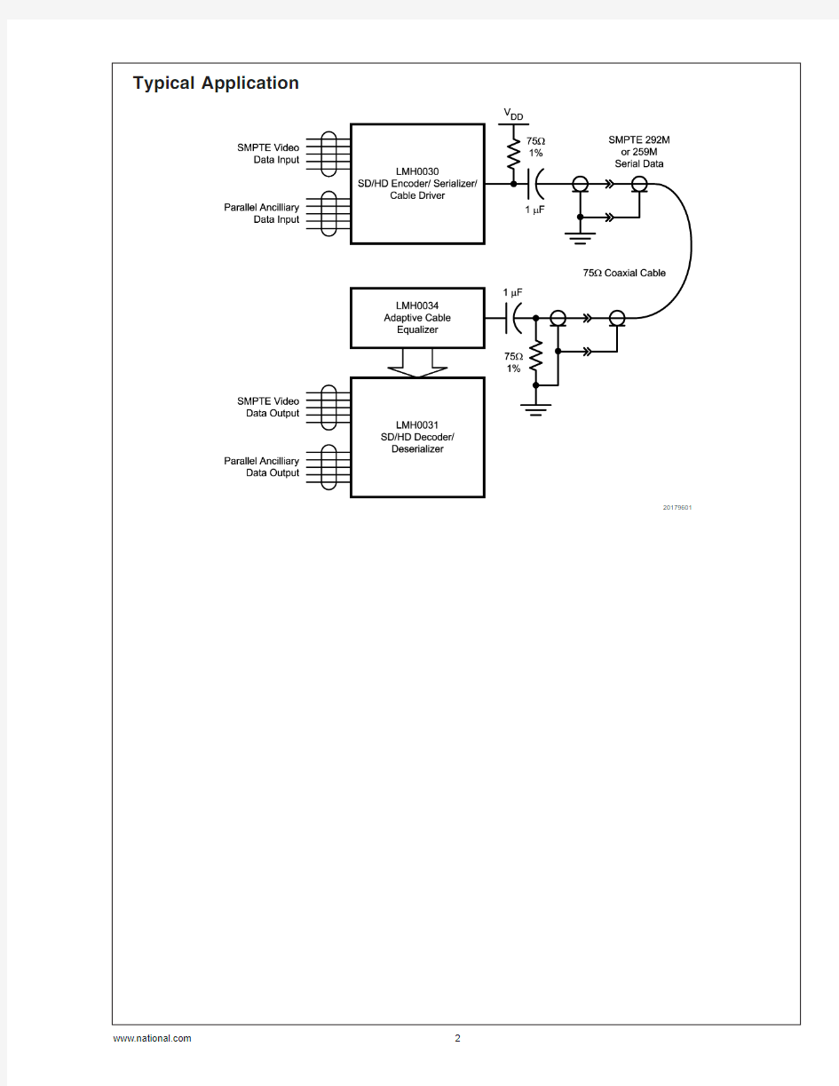
The LMH0030,SMPTE 292M /259M Digital Video Serializer with Ancillary Data FIFO and Integrated Cable Driver,is the ideal complement to the LMH0031.
The LMH0031’s internal circuitry is powered from +2.5Volts and the I/O circuitry from a +3.3Volt supply.Power dissipa-tion is typically 850mW.The device is packaged in a 64-pin TQFP .
Features
n SDTV/HDTV serial digital video standard compliant n Supports 270Mbps,360Mbps,540Mbps,1.483Gbps and 1.485Gbps serial video data rates with auto-detection
n LSB de-dithering option
n Uses low-cost 27MHz crystal or clock oscillator reference
n Fast VCO lock time:<500μs at 1.485Gbps
n Built-in self-test (BIST)and video test pattern generator (TPG)*
n Automatic EDH/CRC word and flag processing n Ancillary Data FIFO with extensive packet handling options
n Adjustable,4-deep parallel output video data FIFO n Flexible control and configuration I/O port
n LVCMOS compatible control inputs and clock and data outputs
n LVDS and ECL-compatible,differential,serial inputs n 3.3V I/O power supply and 2.5V logic power supply operation
n Low power:typically 850mW n 64-pin TQFP package
n Commercial temperature range 0?C to +70?C *Patent applications made or pending.
Applications
n SDTV/HDTV serial-to-parallel digital video interfaces for:—Video editing equipment —VTRs
—Standards converters
—Digital video routers and switchers
—Digital video processing and editing equipment —Video test pattern generators and digital video test equipment
—Video signal generators
Ordering Information
Order Number Package Type NS Package Number
LMH0031VS
64-Pin TQFP
VEC-64A
January 2006
LMH0031SMPTE 292M/259M Digital Video Deserializer /Descrambler with Video and Ancillary Data FIFOs
?2006National Semiconductor Corporation https://www.360docs.net/doc/224651366.html,
Typical Application
20179601
L M H 0031
https://www.360docs.net/doc/224651366.html, 2
LMH0031 Block Diagram
20179602
https://www.360docs.net/doc/224651366.html,
3
Connection Diagram
20179603
64-Pin TQFP
Order Number LMH0031VS See NS Package Number VEC-64A
L M H 0031
https://www.360docs.net/doc/224651366.html, 4
Absolute Maximum Ratings(Note1) It is anticipated that this device will not be offered in a military qualified version.If Military/Aerospace speci-fied devices are required,please contact the National Semiconductor Sales Office/Distributors for availability and specifications.
CMOS I/O Supply Voltage
(V DDIO–V SSIO): 4.0V SDI Supply Voltage
(V DDSI–V SSSI): 4.0V Digital Logic Supply Voltage
(V DDD–V SSD): 3.0V PLL Supply Voltage
(V DDPLL–V SSPLL): 3.0V
CMOS Input Voltage (Vi):V SSIO?0.15V to V DDIO+0.15V
CMOS Output Voltage (Vo):V SSIO?0.15V to
V DDIO+0.15V
CMOS Input Current(single input):
Vi=V SSIO?0.15V:?5mA
Vi=V DDIO+0.15V:+5mA
CMOS Output Source/Sink Current:±6mA
I BB Output Current:+300μA
I REF Output Current:+300μA
SDI Input Voltage
(Vi):
V SSSI?0.15V to
V DDSI+0.15V
Package Thermal Resistance
θJA@0LFM Airflow40.1?C/W
θJA@500LFM Airflow24.5?C/W
θJC 5.23?C/W
Storage Temp.Range:?65?C to+150?C
Junction Temperature:+150?C
Lead Temperature(Soldering4
Sec):+260?C
ESD Rating(HBM): 6.0kV
ESD Rating(MM):400V
Recommended Operating Conditions
Symbol Parameter Conditions Reference Min Typ Max Units V DDIO CMOS I/O Supply Voltage V DDIO?V SSIO
3.150 3.300 3.450V V DDSD SDI Supply Voltage V DDSI?V SSSI
V DDD Digital Logic Supply
Voltage
V DDD–V SSD
2.375 2.500 2.625V
V DDPLL PLL Supply Voltage V DDPLL–V SSPLL
T A Operating Free Air
Temperature
0+70?C
Required Input Conditions
(Note9)
Symbol Parameter Conditions Reference Min Typ Max Units
V IN Input Voltage Range All LVCMOS
Inputs V SSIO V DDIO V
t r,t f Rise Time,Fall Time10%–90% 1.0 1.5 3.0ns
BR SDI Serial Input Data Rate SMPTE259M,Level C
SDI,SDI
270
M BPS SMPTE259M,Level D360
SMPTE344M540
SMPTE292M1,483
SMPTE292M1,485
V CM(SDI)Common Mode Voltage V IN=125mV P-P
SDI,SDI V SSSI
+1.0V
V DDSI
?0.05V
V
V IN(SDI)SDI Serial Input Voltage,
Single-ended
125800880mV P-P V IN(SDI)SDI Serial Input Voltage,
Differential
125800880mV P-P
t r,t f Rise Time,Fall Time 20%–80%,SMPTE259M
Data Rates
0.4 1.0 1.5ns
20%–80%,SMPTE292M
Data Rates
270ps
LMH0031
https://www.360docs.net/doc/224651366.html,
5
Required Input Conditions
(Continued)Symbol Parameter
Conditions
Reference
Min
Typ
Max Units f ACLK Ancillary /Control Data Clock Frequency
A CLK
V CLK
MHz DC ACLK Duty Cycle,Ancillary Clock 455055%t r ,t f
Ancillary /Control Clock and Data Rise Time,Fall Time
10%–90%
1.0
1.5
3.0
ns
t S
Setup Time,AD N to A CLK or IO N to A CLK Rising Edge
Control Data Input or I/O Bus Input
IO N ,AD N ,A CLK Timing Diagram
3.0
1.5ns
t H
Hold Time,Rising Edge A CLK to AD N or A CLK to IO N
3.0
1.5ns
R REF Bias Supply Reference Resistor
Tolerance 1%
4.75k ?f EXT CLK External Clock Frequency Ext Clk
?100ppm
27.0
+100ppm
MHz
f XTAL
Crystal Frequency
Figure 6
XTALo,XTALi
DC Electrical Characteristics
Over Supply Voltage and Operating Temperature ranges,unless otherwise specified (Notes 2,3).Symbol Parameter
Conditions
Reference
Min Typ
Max Units V IH Input Voltage High Level All LVCMOS Inputs
2.0V DDIO V V IL Input Voltage Low Level V SSIO
0.8I IH Input Current High Level V IH =V DDIO (Note 8)+85+150μA
I IL Input Current Low Level V IL =V SSIO ?1?20V OH Output Voltage High Level I OH =?2mA All LVCMOS Outputs
2.4 2.7V DDIO V V OL Output Voltage Low Level I OL =+2mA V SSIO
V SSIO +0.3V SSIO +0.5V
V OHV Minimum Dynamic V OH I OH =?2mA (Note 6)V DDIO ?0.5V OLP Maximum Dynamic V OL I OL =+2mA (Note 6)
V SSIO +0.4V SDI Serial Data Input Voltage SDI,SDI
125
800
880
mV P-P I SDI Serial Data Input Current ±1±10
μA V TH Input Thereshold Over VCM range <100
mV I BB Bias Supply Output Current
R BB =8.66k ?1%?220?188μA
I REF
Reference Output Current R REF =4.75k ?1%?290
?262I DD (3.3V)Power Supply Current,3.3V Supply,Total 270M BPS Data Rate V DDIO ,V DDSI 38.045.0mA 1,485M BPS Data Rate 47.050.0I DD (2.5V)
Power Supply Current,2.5V Supply,Total
270M BPS Data Rate V DDD ,V DDPLL
80120mA
1,485M BPS Data Rate
220
340
L M H 0031
https://www.360docs.net/doc/224651366.html, 6
AC Electrical Characteristics
Over Supply Voltage and Operating Temperature ranges,unless otherwise specified(Note3).
Symbol Parameter Conditions Reference Min Typ Max Units Serial Video Data Inputs
BR SDI Serial Input Data Rate
SMPTE259M,Level C
SDI,SDI 270
M BPS
SMPTE259M,Level D360 SMPTE344M540 SMPTE292M1,483 SMPTE292M1,485
t r,t f Rise Time,Fall Time 20%–80%,SMPTE259M
Data Rates
0.4 1.0 1.5ns 20%–80%,SMPTE292M
Data Rates
270ps
Parallel Video Data Outputs
f VCLK Video Output Clock
Frequency
SMPTE259M,270M BPS
V CLK
27.0
MHz
SMPTE267M,360M BPS36.0
SMPTE344M,540M BPS54.0
SMPTE292M,1,483M BPS74.176
SMPTE292M,1,485M BPS74.25
t pd Propagation Delay,Video
Clock to Video Data Valid
50%–50%
V CLK to DV N
Timing Diagram
0.5 2.0ns
DC V Duty Cycle,Video Clock V CLK50±5%
t JIT Video Data Output Clock
Jitter
27MHz
V CLK
2.0
ns P-P
36MHz 1.4
54MHz 1.0
74.25MHz0.5
Parallel Ancillary/Control Data Inputs,Multi-function Parallel Bus Inputs
f ACLK Ancillary/Control Data
Clock Frequency
A CLK
V CLK MHz
DC A Duty Cycle,Ancillary Data
Clock
ANC Data clock
(Note7)
455055%
t r,t f Output Rise Time,Fall
Time
10%–90%
IO N,AD N,A CLK
Timing Diagram
1.0 1.5 3.0
ns
t S Setup Time,AD N to A CLK
or IO N to A CLK Rising Edge
Control Data Input or I/O
Bus Input
3.0 1.5
t H Hold Time,Rising Edge
A CLK to AD N or A CLK to
IO N
3.0 1.5
Parallel Ancillary/Control Data Outputs
t pd Propagation Delay,Clock
to Control Data
50%–50%
A CLK to AD N
Timing Diagram
8.5
ns
t pd Propagation Delay,Clock
to Ancillary Data
11.5
Multi-function Parallel I/O Bus
t r,t f Rise Time,Fall Time10%–90%IO0–IO7
Timing Diagram
1.0 1.5 3.0ns
PLL/CDR,Format Detect
t LOCK Lock Detect Time SD Rates(Note5)0.32 1.0
ms HD Rates(Note5)0.26 1.0
t FORMAT Format Detect Time All Rates20 Note1:“Absolute Maximum Ratings”are those parameter values beyond which the life and operation of the device cannot be guaranteed.The stating herein of these maximums shall not be construed to imply that the device can or should be operated at or beyond these values.The table of“Electrical Characteristics”
specifies acceptable device operating conditions.
LMH0031
https://www.360docs.net/doc/224651366.html,
7
AC Electrical Characteristics
(Continued)
Note 2:Current flow into device pins is defined as positive.Current flow out of device pins is defined as negative.All voltages are referenced to V SSIO =V SSD =V SSSI =0V.
Note 3:Typical values are stated for V DDIO =V DDSI =+3.3V,V DDD =V DDPLL =+2.5V and T A =+25?C.Note 4:Spec.is guaranteed by design.
Note 5:Measured from rising-edge of first SDI cycle until Lock Detect bit goes high (true).Lock time includes CDR phase acquisition time plus PLL lock time.Note 6:V OHV and V OLP are measured with respect to reference ground.V OLP is the peak output LOW voltage or ground bounce that may occur under dynamic simultaneous output switching conditions.V OHV is the lowest output HIGH voltage or output droop that may occur under dynamic simultaneous output switching conditions.
Note 7:When used to clock control data into or from the LMH0031,the duty cycle restriction does not apply.Note 8:I IH includes static current required by input pull-down devices.
Note 9:Required Input Conditions are the electrical signal conditions or component values which shall be supplied by the circuit in which this device is used in order for it to produce the specified DC and AC electrical output characteristics.
Note 10:Functional and certain other parametric tests utilize a LMH0030as the input source to the SDI inputs of the LMH0031.The LMH0030is DC coupled to the inputs of the LMH0031.Typical V IN =800mV,V CM =2.9V.
Test Loads
20179604
L M H 0031
https://www.360docs.net/doc/224651366.html, 8
LMH0031 Test Circuit
20179607
https://www.360docs.net/doc/224651366.html,
9
Timing Diagram
20179608
Device Operation
INTRODUCTION
The LMH0031SMPTE 292M/259M Digital Video Deserializer/Decoder is used in digital video signal origina-tion and destination equipment:cameras,video tape record-ers,telecines,editors,standards converters,video test and other equipment.It decodes and converts serial SDTV or HDTV component digital video signals into parallel format.The LMH0031decoder/deserializer processes serial digital video (SDV)signals conforming to SMPTE 259M,SMPTE 344M (proposed)or SMPTE 292M and operates at serial data rates of 270Mbps,360Mbps,540Mbps,1.483Gbps and 1.485Gbps.Corresponding parallel output data rates are 27.0MHz,36.0MHz,54.0MHz,74.176MHz and 74.25MHz.
The LMH0031accepts ECL or LVDS serial data input sig-nals.Outputs signals are compatible with LVCMOS logic devices.
Note:In the following explanations,these logical equiva-lences are observed:ON ≡Enabled ≡Set ≡True ≡Logic_1and OFF ≡Disabled ≡Reset ≡False ≡Logic_0.
VIDEO DATA PATH
The Serial Data Inputs (SDI)accept serial video data at SMPTE 259M standard definition,SMPTE 344M (proposed)or SMPTE 292M high-definition data rates.These inputs accept standard ECL or LVDS signal levels and may be used single-ended or differentially.Inputs may be DC or AC coupled,as required,to devices and circuits supplying the data.Recommended operating conditions and all input DC and AC voltage and current specifications shall be observed when designing the input coupling circuits.
For convenience,a reference bias source,pin name R REF ,sets the reference current available from the input bias source,pin name R BB .The recommended nominal value of R REF is 4.75k ?,1%.R BB is provided so that the SDI inputs may be supplied DC bias voltage via external resistors when the inputs are AC-coupled.The bias source should be loaded with a resistance to the V SS supply.The source current available at R BB is 200μA.Figure 1shows a typical input biasing scheme using R BB and R REF .
L M H 0031
https://www.360docs.net/doc/224651366.html, 10
Device Operation(Continued)
The SMPTE descrambler receives NRZI serial data,con-verts it to NRZ,then decodes it to either10-bit standard definition or20-bit high definition parallel video data using the reverse polynomial X9+X4+1as specified in the respective standard:SMPTE259M,SMPTE344M(pro-posed)or SMPTE292M.The data reception bit order is LSB-first.All data processing is done at the parallel rate. The LMH0031incorporates circuitry that implements a method for handling data that has been subjected to LSB dithering.When so enabled,data from the de-scrambler is routed for de-dithering.The De-Dither Enable bit in the VIDEO INFO0control register enables this function.De-dithering of data present in the vertical blanking interval can be selectively enabled by use of the V De-Dither Enable bit in the VIDEO INFO0control register.The initial condition of De-Dither Enable and V De-Dither Enable is OFF.
The descrambler supplies signals to the TRS character de-tector which identifies the presence of the valid video data. The TRS character detector processes the timing refer-ence signals which control raster framing.TRS(sync)char-acters are detected and the video is aligned on word bound-aries.Data is re-synchronized with the parallel word-rate clock.Interraction and operation of the character alignment control signals and indicators Framing Mode,Framing En-able and NSP(New Sync Position)is described later in this datasheet.
The LMH0031implements TRS character LSB-clipping as prescribed in ITU-R BT.601.LSB-clipping causes all TRS characters with a value between000h and003h to be forced to000h and all TRS characters with a value between3FCh and3FFh to be forced to3FFh.Clipping is done after de-scrambling and de-dithering.
Once the PLL attains lock,the video format detector pro-cesses the received data to determine the raster character-istics(video data format)and configure the LMH0031to handle it.This assures that the parallel output data will be properly formatted,that the correct data rate is selected and that Ancillary Data and CRC/EDH data are correctly de-tected and checked.Supported parallel data formats or sub-formats may belong to any one of several component stan-dards:SMPTE125M,SMPTE267M,SMPTE260M,274M, 295M or296M.Refer to Table4for the supported formats. (See also the Section Application Information section for handling of other raster formats or format extensions devel-oped after this device was designed).The detected video standard information is passed to the device control system and saved in the control registers from whence it may be read by the user.
The LMH0031may be configured to operate in a single video format by loading the appropriate FORMAT SET[4:0] control data into the FORMAT0control register.Also,the LMH0031may be configured to handle only the standard-definition data formats by setting the SD ONLY bit or only the high-definition data formats by setting the HD ONLY bit in the FORMAT0control register.When both bits are reset,the default condition,the part automatically detects the data rate and range.
Aligned and de-processed parallel data passes into a variable-depth video FIFO prior to output.Video FIFO depth from0to4registers is set by a3-bit word written into the VIDEO FIFO Depth[2:0]bits in the ANC0control register. The video FIFO permits adjustment of the parallel video data output timing or delay at a parallel word rate.The occurence of corresponding TRS indicator bits,EAV,SAV and NSP,in the control register corresponds to the input register position of the FIFO.This positioning permits a look-ahead function in which the alignment status of the video data can be determined up to four parallel clock periods prior to the appearance of that data at the parallel data output.
The parallel video data is output on DV[19:0].The20-bit parallel video data is organized so that for HDTV data,the upper-order10bits DV[19:10]are luminance(luma)infor-mation and the lower10bits DV[9:0]are colour difference (chroma)information.SDTV data use the lower-order10-bits DV[9:0]for both luma and chroma information.(The SDTV parallel data is also duplicated on DV[19:10]).V CLK is the parallel output word rate clock signal.The frequency of V CLK is appropriate to either the HD or SD data being processed. Data is valid between the falling edges of a V CLK cycle.Data may be clocked into external devices on the rising-edge of V CLK.The DV[19:0]and V CLK signals are LVCMOS-compatible.
20179606
FIGURE1.Optional Input Biasing Scheme
LMH0031
https://www.360docs.net/doc/224651366.html,
11
Device Operation
(Continued)
ANCILLARY/CONTROL DATA PATH
The 10-bit ancillary and Control Data Port AD[9:0]serves two functions in the LMH0031.Ancillary Data from the An-cillary Data FIFO is output from this port after its recovery from the video data stream.The utilization and flow of Ancil-lary Data from the device is managed by a system of control bits,masks and IDs stored in the control data registers.This port also provides read/write access to contents of the con-figuration and control registers.The signals RD/WR ,ANC/CTRL and A CLK control data flow through the port.CONTROL DATA FUNCTIONS
Control data is input to and output from the LMH0031using the lower-order 8bits AD[7:0]of the ancillary/Control Data Port.This control data initializes,monitors and controls op-eration of the LMH0031.The upper two bits AD[9:8]of the port function as handshaking signals with the device access-ing the port.When either a control register read or write address is being written to the port,AD[9:8]must be driven as 00b (0XXh,where XX are AD[7:0]).When control data is being written to the port,AD[9:8]must be driven as 11b (3XXh,where XX are AD[7:0]).When control data is being read from the port,the LMH0031will output AD[9:8]as 10b (2XXh,where XX are output data AD[7:0])and may be ignored by the monitoring system.
Note:After either a manual or power-on reset,A CLK must be toggled three (3)times to complete initiallization of the An-cillary and Control Data Port .
The sequence of clock and control signals for reading control data from the ancillary/control data port is shown in Figure 2.Control data read mode is invoked by making the ANC/CTRL input low and the RD/WR input high.The 8-bit ad-dress of the control register set to be accessed is input to the port on bits AD[7:0].To identify the data as an address,AD[9:8]must be driven as 00b.The complete address word will be 0XXh,where 0is AD[9:8]and XX are AD[7:0].The address is captured on the rising edge of A CLK .When control data is being read from the port,the LMH0031will output AD[9:8]as 10b (2XXh,where XX are output data AD[7:0])and may be ignored by the monitoring system.Data being output from the selected register is driven by the port immediately following the rising edge of A CLK or when the address signal is removed.For optimum system timing,the signals driving the address to the port should be removed
immediately after the address is clocked into the port and before or simultaneously with the falling edge of A CLK at the end of that address cycle.Output data remains stable until the next rising edge of A CLK and may be written into external devices at any time after the removal of the address signal.This second clock resets the port from drive to receive and readies the port for another access cycle.
Example:Read the Full-field Flags via the AD port.1.Set ANC/CTRL to a logic-low.2.Set RD/WR to a logic-high.
3.Present 001h to AD[9:0]as the register address.
4.Toggle A CLK .
5.Release the bus driving the AD port.
6.Read the data present on the AD port.The Full-field
Flags are bits AD[4:0].
7.Toggle A CLK to release the AD port.
Figure 3shows the sequence of clock and control signals for writing control data to the ancillary/control data port.The control data write mode is similar to the read mode.Con-trol data write mode is invoked by making the ANC/CTRL input low and the RD/WR input low.The 8-bit address of the control register set to be accessed is input to the port on bits AD[7:0].When a control register write address is being written to the port,AD[9:8]must be driven as 00b (0XXh,where XX are AD[7:0]).The address is captured on the rising edge of A CLK .The address data is removed on the falling edge of A CLK .Next,the control data is presented to the port bits AD[7:0]and written into the selected register on the next rising edge of A CLK .When control data is being written to the port,AD[9:8]must be driven as 11b (3XXh,where XX are AD[7:0]).Control data written into the registers may be read out non-destructively in most cases.
Example:Setup (without enabling)the TPG Mode via the AD port using the 1125line,30frame,74.25MHz,interlaced component (SMPTE 274M)colour bars as test pattern.The TPG may be enabled after setup using the Multi-function I/O port or by the control registers.1.Set ANC/CTRL to a logic-low.2.Set RD/WR to a logic-low.
3.Present 00Dh to AD[9:0]as the Test 0register address.
4.Toggle A CLK .
5.Present 327h to AD[9:0]as the register data.
6.Toggle A CLK .
L M H 0031
https://www.360docs.net/doc/224651366.html, 12
Device Operation
(Continued)
Ancillary Data Functions
The LMH0031can recover Ancillary Data from the serial data stream.This Ancillary Data and related control charac-ters are defined in the relevant SMPTE standards and may reside in the horizontal and vertical blanking intervals.The data can consist of different types of message packets in-cluding audio data.The serial Ancillary Data space must be formatted according to SMPTE 291M.The LMH0031sup-ports Ancillary Data in the chrominance channel (C’r/C’b)only for high-definition operation.Ancillary Data for standard definition follows the requirements of SMPTE 125M.
The Ancillary Data FIFO is sized to handle a maximum length ANC data Type 1or Type 2packet without the ANC Flag,259words.Defined in SMPTE 291M,the packet con-sists of the Ancillary Data Flag,a 3-word Data ID and Data Count,2558-or 10-bit User Data Words and a Checksum.The design of the LMH0031Ancillary Data FIFO also al-lows storage of up to 8shorter length messages with total length not exceeding 259words including all ID information.Ancillary Data is copied from the data stream into the Ancillary Data FIFO .The parallel Ancillary Data will still be present in the parallel chroma output DV[9:0].ancillary flag information is not extracted into the FIFO.
Copying of ANC data from the video data into the FIFO is controlled by the ANC Mask and ANC ID bits in the control registers.A system of flags,ANC FIFO Empty ,ANC FIFO 90%Full ,ANC FIFO Full and ANC FIFO Overrun are used to monitor FIFO status.The details and functions of these and other control words are explained later in this datasheet.
20179609
FIGURE 2.Control Data Read Timing (2read and 1write cycle shown)
20179610
FIGURE 3.Control Data Write Timing
LMH0031
https://www.360docs.net/doc/224651366.html,
13
Device Operation
(Continued)
Figure 4shows the relationship of clock,data and control signals for reading Ancillary Data from the port AD[9:0].In Ancillary Data read mode,10-bit Ancillary Data is routed from the Ancillary Data FIFO and read from the port AD[9:0]at a rate determined by A CLK .
Ancillary Data read (output)mode is invoked by making the ANC/CTRL input high and the RD/WR input high.Ancillary Data is clocked from the FIFO on the L-H transition of A CLK .Data may be read from the port on rising edges of A CLK ,after the specified propagation delay,until the FIFO is emp-
tied.Data may only be read from the port when in the Ancillary Data mode.Ancillary Data cannot be written to the port.
To conserve power when the Ancillary Data function is not being used,the internal Ancillary Data FIFO clock is dis-abled.This clock must be enabled before Ancillary Data may be replicated into the FIFO for output.This internal FIFO clock is controlled by FIFO CLOCK ENABLE ,bit-6of the ANC 5register (address 17h).The default condition of FIFO CLOCK ENABLE is OFF.After enabling the internal FIFO clock by turning this bit ON,A CLK must be toggled three (3)times to propagate the enable to the clock tree.
MULTI-FUNCTION I/O PORT
The multi-function I/O port can be configured to provide immediate access to many control and indicator functions that are stored within the LMH0031’s configuration and con-trol registers.The individual pins comprising this port are assigned as input or output for selected functions stored in the control data registers.
The multi-function I/O port is configured by way of an 8x6-bit register bank consisting of registers I/O pin 0CONFIG through I/O pin 7CONFIG .The contents of these registers determine whether the port bits function as inputs or outputs and to which control function or indicator each port bit is assigned.Port bits may be assigned to access different functions and indicators or any or all port bits may be as-signed to access the same function or indicator (output mode only).The same indicator or function should not be assigned to more than one port bit as an input.Controls and indicators that are accessible by the port and their corre-sponding selection addresses are given in the I/O Pin Con-figuration Register Addresses,Table 6.Table 2gives the control register bit assignments.
Data resulting from device operation will be sent to the selected I/O port bit.This same data is also stored in the configuration and control registers.Mapping the control and indicator functions in this manner means that device opera-tion will be immediately reflected at the I/O port pins thereby ensuring more reliable real-time operation of the device within and by the host system.
When a multifunction I/O port bit is used as input to a control register bit,data must be presented to the I/O port bit and clocked into the register bit using A CLK as shown in Figure 5.Port timing for bit write operations is the same as for the ANC/CTRL port operation.
Example:Program multi-function I/O port bit-0as the CRC Luma Error bit output.
1.Set ANC/CTRL to a logic-low.
2.Set RD/WR to a logic-low.
3.
Present 00Fh to AD[9:0]as the I/O PIN 0CONFIG register address.4.Toggle A CLK .
5.Present 310h to AD[9:0]as the register data.
6.Toggle A CLK .
EDH/CRC SYSTEM
The LMH0031has EDH and CRC character generation and checking circuitry.The EDH system functions as de-scribed in SMPTE Recommended Practice RP-165.The CRC system functions as specified in SMPTE 292M.The EDH/CRC polynomial generators/checkers accept paral-lel data from the de-serializing system and generate the EDH and CRC check words for comparison with those re-ceived in the data.
The EDH Enable bit in the control register enables the EDH generation and checking system.Incoming SDTV data is checked for errors and the EDH flags are updated automati-20179611
FIGURE 4.Ancillary Data Read Timing
20179612
FIGURE 5.I/O Port Data Write Timing
L M H 0031
https://www.360docs.net/doc/224651366.html,
14
Device Operation(Continued)
cally.EDH errors are reported in the EDH0,EDH1,and EDH2register sets of the configuration and control registers. Updated or new EDH check words and flags may be gener-ated and inserted in the data.EDH check words are gener-ated using the polynomial X16+X12+X6+1per SMPTE RP165.Generation and automatic insertion of new or cor-rected EDH check words is controlled by EDH Force and EDH Enable bits in the control registers.EDH check words and status flags are inserted in the parallel data at the correct positions in the Ancillary Data space and formatted per SMPTE291M.After a reset,the initial state of all EDH and CRC check characters is00h.
The SMPTE292M high definition video standard employs CRC(cyclic redundancy check codes)error checking in-stead of EDH.The CRC consists of two18-bit words gener-ated using the polynomial X18+X5+X4+1per SMPTE 292M.One CRC is used for luminance and one for chromi-nance data.The CRCs appear in the data stream following the EAV and line number characters.The CRCs are checked and errors are reported in the EDH0,EDH1,and EDH2 register sets of the configuration and control registers. PHASE-LOCKED LOOP/CLOCK-DATA RECOVERY SYSTEM
The phase-locked loop and clock-data recovery(PLL/ CDR)system generates all internal timing and data rate clocks for the LMH0031.The PLL/CDR system consists of five main functional blocks:1)the input buffer which receives the incoming data,2)input data samplers which oversample the data coming from the input buffer,3)a PLL(VCO,divider chain,phase-frequency detector and internal loop filter) which generates sampling and other system clocks,4)a digital CDR system to recover the oversampled serial input data from the samplers and the digital system control and5) a rate detect controller which sequences the PLL to find the data rate.
Using an oversampling technique,the timing information encoded in the serial data is extracted and used to synchro-nize the recovered clock and data.The parallel data rate and other clock signals are derived from the regenerated serial clock.The parallel data rate clock is1/10th of the serial data rate clock for standard definition or1/20th of the serial data clock frequency for high definition.The data interface be-tween the CDR and the digital processing block uses10-bit data plus the required clocks.
The PLL is held in coarse frequency lock by an external 27MHz clock signal,EXT CLK,or by an external27MHz crystal and internal oscillator.Upon power-on,EXT CLK is the default reference.The internal oscillator and an external crystal may be used as the reference by setting the OSCEN bit in the CDR register.The reference clock reduces lock latency and enhances format and auto-rate detection robust-
ness.PLL acquisition,data phase alignment and format
detection time is20ms or less at1.485Mbps.The VCO has
separate V DDPLL and V SSPLL power supply feeds,pins51
and52,which may be supplied power via an external low-
pass filter,if desired.
A27MHz crystal and load circuit may be used to provide the
reference clock.A fundamental mode crystal with the follow-
ing parameters is used:frequency27MHz,frequency toler-
ance±30ppm,load capacitance18pF,maximum drive level
100μW,equivalent series resistance<50?,operating tem-
perature range0?C to70?C.Refer to Figure6for a typical
load circuit and connection information.
The LMH0031indicates that the PLL is locked to the incom-
ing data rate and that the CDR has acquired a phase of the
serial data by setting the Lock Detect bit in the Video Info0
control register.Indication of the standard being processed
is retained in the FORMAT[4:0]bits in the FORMAT1con-
trol data register.Format data from this register can be
programmed for output on the multi-function I/O port.The
power-on default assigns Lock Detect as I/O Port bit4.
POWER SUPPLIES,POWER-ON-RESET AND RESET
INPUT
The LMH0031requires two power supplies,2.5V for the core
logic functions and3.3V for the I/O functions.The supplies
must be applied to the device in proper sequence.The3.3V
supply must be applied prior to or coincident with the2.5V
supply.Application of the2.5V supply must not precede the
3.3V supply.It is recommended that the3.3V supply be
configured or designed so as to control application of the
2.5V supply in order to satisfy this sequencing requirement.
The LMH0031has an automatic,power-on-reset circuit.
Reset initializes the device and clears TRS detection cir-
cuitry,all latches,registers,counters and polynomial
generators/checkers and resets the EDH/CRC characters to
00h.An active-HIGH-true,manual reset input is available at
pin49.The reset input has an internal pull-down device and
may be considered inactive when unconnected.
Important:When power is first applied to the device or
following a reset,the ancillary and Control Data Port must
be initialized to receive data.This is done by toggling A CLK
three times.
20179605
FIGURE6.Crystal and Load Circuit
LMH0031
https://www.360docs.net/doc/224651366.html,
15
Device Operation
(Continued)
TEST PATTERN GENERATOR (TPG)AND BUILT-IN SELF-TEST (BIST)
The LMH0031includes an on-board,parallel video test pat-tern generator (TPG).Four test pattern types are available in both HD and SD formats,NTSC and PAL standards,and 4x3and 16x9raster sizes.The test patterns are:flat-field black,PLL pathological,equalizer (EQ)pathological and a 75%,8-colour vertical bar pattern.The pathologicals follow recommendations contained in SMPTE RP 178-1996re-garding the test data used.The colour bar pattern has op-tional bandwidth limiting coding in the chroma and luma data transitions between bars.The VPG FILTER ENABLE bit in the VIDEO INFO 0control register enables the colour bar filter function.The test pattern data is available at the video data outputs,DV[19:0]with a corresponding parallel rate clock,VCLK ,appropriate to the particular standard and format selected.
The TPG also functions as a built-in self-test (BIST)which can be used to verify device functionality.The BIST function performs a comprehensive go/no-go test of the device.The test may be run using any of the HD colour bar patterns or one of two SD patterns,either the 270Mb/s NTSC colour bar or the PAL PLL pathological,as the test data pattern.Data is input from the digital processing block,processed through the device and tested for errors using either the EDH system for SD or the CRC system for HD.Clock signals from the CDR block supply timing for the test data.The CDR must be supplied a 27MHz reference clock via the XTALi/Ext Clk input (or using the internal oscillator and crystal)during the TPG or BIST function.A go/no-go indication is logged in the Pass/Fail bit of the TEST 0control register set.This bit may be assigned as an output on the multifunction I/O port.
TPG and BIST operation is initiated by loading the code for the desired test pattern into the Test Pattern Select[5:0]bits and by setting the TPG Enable bit of the TEST 0register.Note that when attempting to use the TPG or BIST immedi-ately after the device has been reset or powered on,the TPG defaults to the 270Mbps SD rate.The device must be con-figured for the desired test pattern by loading the appropriate code in to the TEST 0register.If HD operation is desired,
selection of the desired HD test pattern is sufficient to enable the device to configure itself to run at the correct rate and generate valid data.Table 5gives the available test patterns and codes.
The Pass/Fail bit in the control register gives the device test status indication.If no errors have been detected,this bit will be set to logic-1approximately 2field intervals after TPG Enable is set.If errors have been detected in the internal circuitry of the LMH0031,Pass/Fail will remain reset to a logic-0.TPG or BIST operation is stopped by resetting the TPG Enable bit.Parallel output data is present at the DV[19:0]outputs during TPG or BIST operation.
Example:Enable the TPG Mode to use the NTSC 270Mbps colour bars as the BIST and TPG pattern.Enable TPG operation using the I/O port.
1.Set ANC/CTRL to a logic-low.
2.Set RD/WR to a logic-low.
3.Present 00Dh to AD[9:0]as the TEST 0register ad-dress.
4.Toggle A CLK .
5.
Present 343h to AD[9:0]as the register data (525line,30frame,27MHz,NTSC 4x3,colour bars (SMPTE 125M)).
6.Toggle A CLK .
7.The PASS/FAIL indicator,TEST 0register,Bit 7,should
be read for the result of the test.Alternatively,this bit may be mapped to a convenient bit of the Multi-function I/O bus.The test pattern data and clock is available at the DV[19:0]and V CLK outputs.CONFIGURATION AND CONTROL REGISTERS
The configuration and control registers store data which determines the operational modes of the LMH0031or which result from its operation.Many of these registers may be assigned as external I/O functions which are then available on the multi-function I/O bus.These functions are summa-rized in Table 1and detailed in Table 2.The power-on default condition for the multi-function I/O port is indicated in Table 1and detailed in Table 6.
L M H 0031
https://www.360docs.net/doc/224651366.html, 16
Device Operation(Continued)
TABLE1.Configuration and Control Data Register Summary
Register Function Bits Read or Write Initial Condition Available on
I/O Bus
Notes
EDH and CRC Operations
CRC Error(SD/HD)1R Reset Output(Note11)I/O5
CRC Error Luma1R Reset Output
CRC Error Chroma1R Reset Output
CRC Replace1R/W OFF No(Note13)
Full-Field Flags5R Reset No
Active Picture Flags5R Reset No
ANC Flags5R Reset No
EDH Force1R/W OFF Input
EDH Enable1R/W ON Input
F/F Flag Error1R Reset Output
A/P Flag Error1R Reset Output
ANC Flag Error1R Reset Output
Ancillary Data Operations
ANC Checksum Force1R/W OFF Input
ANC Checksum Error1R Reset Output
ANC FIFO Empty1R Set Output(Note11)I/O6
ANC FIFO90%Full1R Reset Output
ANC FIFO Full1R Reset Output
ANC FIFO Overrun1R Reset Output
ANC ID16R/W0000h No
ANC Mask16R/W FFFFh No
MSG Track1R/W OFF No
MSG Flush Static1R/W OFF No
FIFO Flush Static1R/W OFF No
Full MSG Available1R OFF Output
Short MSG Detect1R OFF Output
FIFO Clock Enable1R/W OFF No
FIFO Extract Enable1R/W OFF Input
Video FIFO Operation
Video FIFO Depth3R/W000b No
Video Format Operations
Format Set5R/W00000B No
SD Only1R/W OFF No
HD Only1R/W OFF No
Format5R Output Format[4](Note11)
I/O3
H1R Output(Note11)I/O2
V1R Output(Note11)I/O1
F1R Output(Note11)I/O0
Framing Mode1R/W ON No
Framing Enable1R/W ON Input
New Sync Position(NSP)1R Output
SAV1R Output
EAV1R Output(Note11)I/O7
De-scramble Enable1R/W ON No
NRZI Enable1R/W ON No
LMH0031
https://www.360docs.net/doc/224651366.html,
17
Device Operation
(Continued)
TABLE 1.Configuration and Control Data Register Summary (Continued)
Register Function Bits Read or Write
Initial Condition
Available on I/O Bus
Notes
LSB Clipping Enable 1R/W ON No Sync Detect Enable 1R/W ON No De-Dither Enable 1R/W OFF Input Vert.De-Dither Enable 1R/W OFF
Input Lock Detect 1R Output (Note 11)I/O 4Unscrambled Video Data Out
1
R/W
OFF No
(Note 13)
TPG and BIST Operations Test Pattern Select 6R/W 000000b Input 525/27MHz/Black
TPG Enable 1R/W OFF Input Pass/Fail
1R Output VPG Filter Enable
1R/W OFF Input Reference Clock Operations Reference Clock 2R/W 00b No EXT CLK Enabled External Vclk 1R/W OFF No (Note 13)
Multifunction I/O Bus Operations
I/O Bus Pin Config.
48
R/W
See Table 6
No
Note 11:Connected to multifunction I/O port at power-on.
Note 12:ON =SET =logic-1,OFF =RESET =logic-0(positive logic).Note 13:Special or restricted functionality.Refer to text for details.
TABLE 2.Control Register Bit Assignments
Bit 7Bit 6Bit 5Bit 4Bit 3Bit 2Bit 1Bit 0EDH 0(register address 01h)CRC ERROR EDH FORCE EDH ENABLE F/F UES
F/F IDA
F/F IDH
F/F EDA
F/F EDH
EDH 1(register address 02h)
CRC REPLACE CRC ERROR
LUMA CRC ERROR CHROMA A/P UES
A/P IDA
A/P IDH
A/P EDA
A/P EDH
EDH 2(register address 03h)
F/F FLAG ERROR
A/P FLAG ERROR
ANC FLAG ERROR
ANC UES
ANC IDA
ANC IDH
ANC EDA
ANC EDH
ANC 0(register address 04h)
VIDEO FIFO-DEPTH(2)VIDEO FIFO-DEPTH(1)VIDEO
FIFO-DEPTH(0)ANC FIFO OVERRUN
ANC FIFO EMPTY
ANC FIFO FULL
ANC CHECK-SUM ERROR ANC CHECK-SUM FORCE
ANC 1(register address 05h)ANC ID(7)ANC ID(6)ANC ID(5)ANC ID(4)ANC ID(3)ANC ID(2)ANC ID(1)ANC ID(0)ANC 2(register address 06h)ANC ID(15)
ANC ID(14)
ANC ID(13)
ANC ID(12)ANC ID(11)ANC ID(10)ANC ID(9)ANC ID(8)ANC 3(register address 07h)ANC MASK(7)
ANC MASK(6)
ANC MASK(5)
ANC MASK(4)ANC MASK(3)ANC MASK(2)ANC MASK(1)ANC MASK(0)ANC 4(register address 08h)ANC MASK(15)ANC MASK(14)ANC MASK(13)
ANC MASK(12)
ANC MASK(11)
ANC MASK(10)
ANC MASK(9)
ANC MASK(8)
ANC 5(register address 17h)
FIFO EXTRACT ENABLE
FIFO CLOCK ENABLE
FULL MSG AVAILABLE
reserved
FIFO FLUSH STATIC
reserved
MSG FLUSH STATIC
MSG TRACK
L M H 0031
https://www.360docs.net/doc/224651366.html, 18
Device Operation(Continued)
TABLE2.Control Register Bit Assignments(Continued)
Bit7Bit6Bit5Bit4Bit3Bit2Bit1Bit0 ANC6(register address18h)
ANC FIFO 90%FULL SHORT MSG
DETECT
ANC PARITY
MASK
reserved reserved reserved reserved VANC
FORMAT0(register address0Bh)
FRAMING MODE SD ONLY HD ONLY
FORMAT
SET(4)
FORMAT
SET(3)
FORMAT
SET(2)
FORMAT
SET(1)
FORMAT
SET(0)
FORMAT1(register address0Ch)
F V H FORMAT(4)FORMAT(3)FORMAT(2)FORMAT(1)FORMAT(0) TEST0(register address0Dh)
PASS/FAIL TPG ENABLE
TEST
PATTERN
SELECT(5)
TEST
PATTERN
SELECT(4)
TEST
PATTERN
SELECT(3)
TEST
PATTERN
SELECT(2)
TEST
PATTERN
SELECT(1)
TEST
PATTERN
SELECT(0)
VIDEO INFO0(register address0Eh)
DE-DITHER ENABLE
VERT.
DE-DITHER
ENABLE
VPG FILTER
ENABLE
LOCK
DETECT
EAV SAV NSP
FRAMING
ENABLE
VIDEO CONTROL0(register address55h)
reserved EXTERNAL
V CLK
SYNC DETECT
ENABLE
LSB CLIP
ENABLE
reserved
NRZI
ENABLE
DE-Scramble
ENABLE
reserved
REFERENCE CLOCK(register address67h)
reserved reserved reserved reserved reserved INT_OSC EN CLK EN reserved
MULTI-FUNCTION I/O BUS PIN CONFIGURATION
I/O PIN0CONFIG(register address0Fh)
reserved reserved PIN0SEL[5]PIN0SEL[4]PIN0SEL[3]PIN0SEL[2]PIN0SEL[1]PIN0SEL[0]
I/O PIN1CONFIG(register address10h)
reserved reserved PIN1SEL[5]PIN1SEL[4]PIN1SEL[3]PIN1SEL[2]PIN1SEL[1]PIN1SEL[0]
I/O PIN2CONFIG(register address11h)
reserved reserved PIN2SEL[5]PIN2SEL[4]PIN2SEL[3]PIN2SEL[2]PIN2SEL[1]PIN2SEL[0]
I/O PIN3CONFIG(register address12h)
reserved reserved PIN3SEL[5]PIN3SEL[4]PIN3SEL[3]PIN3SEL[2]PIN3SEL[1]PIN3SEL[0]
I/O PIN4CONFIG(register address13h)
reserved reserved PIN4SEL[5]PIN4SEL[4]PIN4SEL[3]PIN4SEL[2]PIN4SEL[1]PIN4SEL[0]
I/P PIN5CONFIG(register address14h)
reserved reserved PIN5SEL[5]PIN5SEL[4]PIN5SEL[3]PIN5SEL[2]PIN5SEL[1]PIN5SEL[0]
I/O PIN6CONFIG(register address15h)
reserved reserved PIN6SEL[5]PIN6SEL[4]PIN6SEL[3]PIN6SEL[2]PIN6SEL[1]PIN6SEL[0]
I/O PIN7CONFIG(register address16h)
reserved reserved PIN7SEL[5]PIN7SEL[4]PIN7SEL[3]PIN7SEL[2]PIN7SEL[1]PIN7SEL[0]
LMH0031
https://www.360docs.net/doc/224651366.html,
19
Device Operation
(Continued)
TABLE 3.Control Register Addresses
Register Name
Address Hexadecimal
EDH 001EDH 102EDH 203ANC 004ANC 105ANC 206ANC 307ANC 408ANC 517ANC 618FORMAT 00B FORMAT 10C TEST 00D VIDEO INFO 00E I/O PIN 0CONFIG 0F I/O PIN 1CONFIG 10I/O PIN 2CONFIG 11I/O PIN 3CONFIG 12I/O PIN 4CONFIG 13I/O PIN 5CONFIG 14I/O PIN 6CONFIG 15I/O PIN 7CONFIG 16VIDEO CONTROL 055VIDEO CONTROL 156REFERENCE CLOCK
67
EDH 0(register 01h)
The EDH Full-Field flags F/F UES ,F/F IDA ,F/F IDH ,F/F EDA and F/F EDH are defined in SMPTE RP 165.The flags are updated automatically when the EDH function is enabled and data is being received.
The EDH ENABLE bit,when set,enables operation of the EDH generator function during SD operation.The default condition of this bit is set (ON).
The EDH FORCE bit,when set,causes updated EDH pack-ets to be inserted in the parallel output data regardless of the previous condition of EDH checkwords and flags in the input serial data.This function may be used in situations where video content has been edited thus making the previous EDH information invalid.The default condition of this bit is reset (OFF).
The CRC ERROR bit indicates that errors in either the EDH checksums (SD)or CRC checkwords (HD)were detected in the serial input data.This bit is a combined function which indicates the presence of either EDH errors during SD op-eration or CRC errors during HD operation.
EDH 1(register 02h)
The EDH Active Picture flags A/P UES ,A/P IDA ,A/P IDH ,A/P EDA and A/P EDH are defined in SMPTE RP 165.The flags are updated automatically when the EDH function is enabled and data is being received.
Specific types of CRC errors in incoming HD serial data are reported in the CRC ERROR LUMA and CRC ERROR CHROMA bits.
The CRC REPLACE bit,when set,causes the CRCs in the incoming data to be replaced with CRCs calculated by the LMH0031.The bit is normally reset (OFF).
EDH 2(register 03h)
The EDH Ancillary Data flags ANC UES ,ANC IDA ,ANC IDH ,ANC EDA and ANC EDH are defined in SMPTE RP 165.The flags are updated automatically when the EDH function is enabled and data is being received.
The status of EDH flag errors in incoming SD serial data are reported in the ffFlagError ,apFlagError and ancFlagError bits.Each of these bits is the logical-OR of the correspond-ing EDH and EDA flags.
ANC 0(Address 04h)
The V FIFO Depth[2:0]bits control the depth of the video FIFO which preceeds the parallel output data drivers.The depth can be set from 0to 4stages by writing the corre-sponding binary code into these bits.For example:to set the Video FIFO depth at two registers,load 11010XXXXXb into the ANC 0control register (where X represents the other functional bits of this register).
Note:When changing some but not all bits in a register and to retain unchanged other data previously stored in the register,read the register’s contents and logically-OR this with the new data.Then write the modified data back into the register.
Flags for ANC FIFO EMPTY ,ANC FIFO 90%FULL ,ANC FIFO FULL and ANC FIFO OVERRUN are available in the configuration and control register set.These flags can also be assigned as outputs on the multi-function I/O port.ANC FIFO EMPTY when set indicates that the FIFO contains no data.ANC FIFO 90%FULL indicates when the FIFO is at 90%of capacity.Since it is virtually impossible for the host processor to begin extracting data from the FIFO after it has been flagged as full without the possibility of an overrun condition occurring,ANC FIFO 90%FULL is used as an advanced command to the host to begin extracting data from the FIFO.To be used properly,ANC FIFO 90%FULL should be assigned as an output on the multi-function I/O port and monitored by the host system.Otherwise,inadvertent loss of ancillary packet data could occur.ANC FIFO FULL when set indicates that the FIFO registers are completely filled with data.
The ANC FIFO OVERRUN flag indicates that an attempt to write data into a full FIFO has occurred.ANC FIFO OVER-RUN can be reset by reading the bit’s status via the ancillary/Control port.If an overrun occurrs,the status of the FIFO message tracking will be invalidated.In this event,the FIFO should be flushed to reset the message tracking pointers.Any messages then in the FIFO will be lost.
The ANC Checksum Force bit,under certain conditions,enables the overwriting of Ancillary Data checksums re-ceived in the data.Calculation and insertion of new Ancillary Data checksums is controlled by the ANC Checksum Force bit.If a checksum error is detected (calculated and received checksums do not match)and the ANC Checksum Force bit is set,the ANC Checksum Error bit is set and a new checksum is inserted in the Ancillary Data replacing the previous one.If a checksum error is detected and the ANC Checksum Force bit is not set,the checksum mismatch is
L M H 0031
https://www.360docs.net/doc/224651366.html,
20
IC-HK_datasheet
Rev 21.11.01, Page 1/13 current of 100mA pulse current of 100mA Fig. 2: Signal patterns for Example 1 -pulse current of 100mA APPLICATION NOTES Setting the laser current When switching DC currents of up to 150mA or pulse currents of up to 700mA one channel is sufficient (Example 1). Input ENx of the unused channel should be jumpered to GND and pin AGNDx left open. Higher currents or several different current levels can be obtained by using both channels (Example 2 and 3).Example 1:Switching a current of 100mA 1. 100mA < 150mA | one channel 2. Switching on and off only | RK can be omitted (RK = 0S ) 3. As shown in Figure 1 (cf. data sheet, Figures 2..4), the required voltage V(CI) for RK = 0S is read off at I(LDK) = 100mA as V(CI) =1.75V With the circuit shown in Figure 3 and a voltage of 1.75V at pin CI the laser current can be switched between typically 0mA and 100mA by applying an appropriate pulse pattern to EN1.
芯片数据手册Datasheet热门问题
芯片数据手册Datasheet热门问题 ?如何正确的阅读Datasheet? 不仅仅是芯片,包括工具、设备几乎任何电子产品,都需要去阅读它的datasheet,除了包括最低、最高要求,特点,建议和用途及其兼容的设备等等,更重要的是原厂商以一个成功者的身份去告诉你一些注意事项。 Datasheet一般组成的字段:(LM317举例) ①日期:首先检查发布日期,是预备版还是修正版 ②厂商:检查厂商,因为相同型号不同厂商的器件,性能或许不同 ③描述(Description):往往会告诉你一些一般地方没有提到的功能或者用法。比如:你可能需要保持一个特殊的引脚为低电平才能完成某个操作。 ④特点(Features):告诉你常规特征。确认电器特征相应的条件 ⑤应用(Application):通常简洁的告诉你该器件是否在你的应用领域;如果这个芯片有你需要的功能,它可以给予你很好的提示。但是这里给出的功能往往都是很一般(常用)的功能 ⑥封装图:不同的封装引脚的位置一般不同,但引脚的总是一般是相同的,需要注意不同位置的引脚及其每个引脚的功能 ⑦性能坐标图:通常描述电流测量与电压的变化曲线,通常会标明25℃(室温) ⑧电气特性表格:通常是芯片参数-条件-变化范围的表格,即相同参数条件不同,输出范围在Min-Typ-Max 之间 ?是不是所有芯片都有Datasheet? 理论上所有芯片都有它对应的datasheet,但是有些芯片是属于定制器件,例如:手机、PC、PAD里面的芯片。往往原厂商只公开它的一般描述、一般特点、一般应用,少许的会公开参数,所以像这样的datasheet 我们正常是拿不到的,这就是为什么有时候一款芯片我们翻江倒海,翻山越岭也没找到的原因了,不过也有些芯片可以通过向原厂商提交申请,审核通过后会提供给你。 ?职业不同如何避轻就重去读Datasheet? 当我们用到datasheet时,有时候没必要从头读到尾,那样会花费大量的时间。Datasheet中涉及到芯片的方方面面,硬件、软件、工艺、制程技术、封装等等,学会抓住关键字词,了解我们所需要的信息,比如:我们想了解AO4459这款P沟道场效应MOSFET ①如果咱们是做硬件,需主要关注Drain-Source Voltage(漏源电压), Gate-Source Voltage(门源电压), Continuous Drain Current(连续漏电流),Pulsed Drain Current(漏电流脉冲)等等,能够看懂热特性曲线图(TYPICAL ELECTRICAL AND THERMAL CHARACTERISTICS);
如何看datasheet+8页(绝对有用)
How to Read a Datasheet Prepared for the WIMS outreach program 5/6/02, D. Grover In order to use a PIC microcontroller, a flip-flop, a photodetector, or practically any electronic device, you need to consult a datasheet. This is the to. Where do you find datasheets? Nowadays you can find almost any datasheet on the internet, often in PDF (Acrobat) form. For example, the LM555 datasheet from National Semiconductor is on their website at https://www.360docs.net/doc/224651366.html,.
LM555Timer General Description The LM555is a highly stable device for generating accurate time delays or oscillation.Additional terminals are provided for triggering or resetting if desired.In the time delay mode of operation,the time is precisely controlled by one external re-sistor and capacitor.For astable operation as an oscillator,the free running frequency and duty cycle are accurately controlled with two external resistors and one capacitor.The circuit may be triggered and reset on falling waveforms,and the output circuit can source or sink up to 200mA or drive TTL circuits. Features n Direct n Timing n Operates n Adjustable n Output n Output n Temperature n Normally n Available Applications n Precision n Pulse n Sequential DS007851-1 有时常规描述(General Description )会给出一些其它地方没提到的特性或者用法。特性(确认电气特性所在的条件以及特殊情况。 通常叫做等效原理图,该原理不是该芯片中必须的,但是该芯片将按照里面的来运作。它能帮助解释在数据手册中未被描述的行为。能把这个电路在面包板上搭出来吗?除非您知道那些并未给出参数的晶体管的参数。 总会有一个日期。数据手册变动,尤其是预备版或者修正版,核对一下日期。
常用的十大电子元器件Datasheet
常用的十大电子元器件Datasheet 元器件数据表(datasheet)是电子工程师项目开发时经常使用到的手册。Datasheet(数据手册)包含了电子芯片的各项参数,电性参数,物理参数,甚至制造材料,使用建议等,一般由厂家编写,内容形式一般为说明文字,各种特性曲线,图表,数据表等。下面介绍一下常用的十大电子元件: 1、DS18B20温度传感器273W百度收录总数 常用指数:★★★★★ DS18B20是Dallas公司生产的数字温度传感器,具有体积小、适用电压宽、经济灵活的特点。它内部使用了onboard专利技术,全部 传感元件及转换电路集成在一个形如三极管的集成电路内。DS18B20有电源线、地线及数据线3根引脚线,工作电压范围为3~5.5 V ,支持单总线接口。 免费下载:DS18B20 2、TL431可控精密稳压源244W 常用指数:★★★★ TL431是由德州仪器生产,所谓TL431就是一个有良好的热稳定性能的三端可调分流基准源。它的输出电压用两个电阻就可以任意地 设置到从Vref(2.5V)到36V范围内的任何值(如图1)。该器件的典型动态阻抗为0.2Ω,在很多应用中可以用它代替齐纳二极管,例如, 数字电压表,运放电路、可调压电源,开关电源等等。 免费下载:TL431
LM358双运算放大器238W 常用指数:★★★★ LM358双运算放大器,适合于电源电压范围很宽的单电源使用,也适用于双电源工作模式,在推荐的工作条件下,电源电流与电源电压无关。它的使用范围包括传感放大器、直流增益模块和其他所有可用单电源供电的使用运算放大器的场合。 免费下载:LM358 4、LM324四路运算放大器236W 常用指数:★★★★ LM324系列是低成本的四路运算放大器,具有真正的差分输入。在单电源应用中,它们与标准运算放大器类型相比具有几个明显的优 势。该四路放大器可以工作于低至3.0 V或高达32 V的电源电压,静态电流是MC1741的五分之一左右(每个放大器)。共模输入范围 包括负电源,因此在众多应用中无需外部偏置元器件。输出电压范围也包括负电源电压。免费下载:LM324 5、DAC0832数模转换芯片157W 常用指数:★★★ DAC0832是8分辨率的D/A转换集成芯片。与微处理器完全兼容。这个DA芯片以其价格低廉、接口简单、转换控制容易等优点,在单 片机应用系统中得到广泛的应用。D/A转换器由8位输入锁存器、8位DAC寄存器、8位D/A转换电路及转换控制电路构成。 免费下载:DAC0832
IP178D 芯片datasheet
IP178D
Preliminary Data Sheet
8 Port 10/100 Ethernet Integrated Switch
(Port Mirror, TCP/UDP QoS & VIP Port QoS)
Features
Wide operating temperature range IP178D LF (0°C to 70°C) IP178D LFI (-40°C to 85°C) IP178C pin to pin compatible Support 2k MAC address Support auto-polarity for 10 Mbps Support filter/forward special DA option Support broadcast storm protection Auto MDI-MDIX option Two queues per port for QoS purposes Support Port based QoS Support 802.1p & DiffServ based QoS QoS Port base 802.1p IP DiffServ IPV4/IPV6 TCP/UDP port number Pins configure ports priority (VIP port) Support max forwarding packet length 1552/1536 bytes option Support port mirror function Support two dynamic fiber ports for Hot Plug Built in linear regulator control circuit Support Lead Free package (Please refer to the Order Information) 0.16um Process
General Description
IP178D integrates an 8-port switch controller, SSRAM, and 8 10/100 Ethernet transceivers. Each of the transceivers complies with the IEEE 802.3, IEEE 802.3u, and IEEE 802.3x specifications. The transceivers are designed in DSP approach in 0.16um technology; they have high noise immunity and robust performance. IP178D supports a lot of QoS function, including 802.1p, DiffServ, TCP/UDP port number and High priority port. User could enable QoS function from Pin or EEPROM. IP178D also supports port mirror function for each port. User could monitor RX and TX port. There are two fiber ports, port 6 and port 7, could be enable and disable from pin.
1 / 56 Copyright ? 2007, IC Plus Corp.
December 23, 2008 IP178D-DS-R01
ALLDATASHEET
ALLDATASHEET是全球电子元器件数据手册库,在这里你可以搜索到近两千万个电子元器件型号的数据。万联芯城是国内知名的电子元器件采购网,专为客户提供一站式电子元器件配单服务,所售电子元器件均为原装现货,满足客户所有物料需求。点击进入万联芯城 点击进入万联芯城
ALLDATASHEET是全球电子元器件数据手册库,提供了近2000万个元器件型号的PDF数据手册,声称“如果在本站没有找到,那么别的地方不可能再有”。ALLDATASHEET强大的资源搜集能力让它成为电子工程师的必备网站,在这里他们可以找到他们想要的一切资料,并完成他们的研发。 ALLDATASHEET每一份数据手册对应的型号出自其原厂,不管是固件工程师、硬件研发人员亦或者板子维修员,想要用最快、最省时间的方法去了解一个芯片,那么,无疑是从ALLDATASHEET去寻找。ALLDATASHEET内的芯片手册,会因为从事的行业不同,而关注不同的点。当然,如果你还没正式工作,只是一名学生的话,这本科技英语非常的适合你阅读。 一般ALLDATASHEET会先从芯片特性到应用场合,最后到内部框架去了解。当然,这里所指的了解是宏观的,对于芯片这种注重细节的物件,微观上才是让我们兴奋的点。芯片参数、管脚定义、内部寄存器任何一个都要研究透彻。连手册中的注意部分都不要放过。 我更偏向于将你们所称谓的ALLDATASHEET当作是一个说明书来读,一般的芯片指导书太过拗口,而说明书为了让使用者看懂,除了专业词汇,都尽量的使用了通俗易懂的语句。尽管如此,想要看懂一个元
器件厂商所写的数据手册,首先你还是要具备一定的英语、电气技术(电子技术、电气)、微机原理技能。一个不懂OC的人是无法看懂数 据手册的。 假设,你在犹豫入手某一块MOS管芯片,你在ALLDATASHEET下载好 对应的数据手册后,首先,要浏览的是简介!很多人以为简介只是介 绍厂家信息及芯片数据,从简介中你能够知道该芯片功能及应用范围,包括输入输出的电流电压、功率大小、工作温度等。MOS管芯片一般涉及电源及驱动,也就是电气特性,你需要从手册中了解这方面的信息,看是否符合你所使用的范围,这些在ALLDATASHEET网站中都能 帮到你。
NK510超外差接收芯片Datasheet
NK51 产品特征 ● 300MHz 到440MHz 的频率范围 ● 工作电压:2.2V-3.6V ● 接受灵敏度高:-110dBm ● 数据传输速率达10kbps (固定模式) ● 低功耗 ? 315MHz 下,最大工作电流2mA 433MHZ 下,最大工作电流2.5mA ? 关闭时的电流为0.9uA ? 扫描操作时(10:1任务周期操作) 电流为300uA ● 唤醒输出标记用来启动解码器和微处理器 ● 天线处的射频辐射非常低 ● 集成度高,外部器件需求少 应用领域 ● 汽车远程无钥匙进入(RKE ) ● 远程控制 ● 远程风扇和电灯控制 ● 车库门和门禁控制 0是一个ASK/OOK (开关键控)的单晶片射频接收集成电路设备。它是一个真正的“从天线接收到数据输出”的单片电路。所有的射频和中频的调谐都在集成电路里完成,这样可以无须手动调整并且降低成本。实现了一个高度可靠且低成本的解决方案。是一个采用16引脚封装且功能齐全的芯片,A/B/C/DL 采用了8引脚封装,功能稍有减少。 提供了两种附加的功能,(1)一个关闭引脚,在任务周期操作时可以用来关闭设备;(2)一个唤醒输出引脚,当接收到射频信号时,它可以提供一个输出标记。这些特点使得可以用在低功耗的应用上,比如RKE 和远程控制。 上提供了所有的中频滤波和数据解调滤波器,所以,不需要外部的滤波器了。四个解调滤波器的带宽可以由用户从外部控制。 提供了两种工作模式:固定模式(FIX )和扫描模式(SWP )。在固 定模式中,用作传统的超外差接收器。在扫描模式下,在一个较宽的射频范围内进行扫描。固定模式提供了更有选择性和针对性的工作模式,并且使得可以与低成本,精确度较低的发射器一起使用。 NK51 0 NK51 0NK51 0NK51 0NK51 0NK51 0NK51 0NK51 0NK51 0NK51 0
降压稳压芯片LSP5502DATASHEET
PIN ASSIGNMENT SS EN COMP FB BS IN SW GND SOP-8L PIN DESCRIPTION Name No. Description BS 1 Bootstrap. This pin acts as the positive rail for the high-side switch’s gate driver. Connect a 0.01uF capacitor between BS and SW. IN 2 Input Supply. Bypass this pin to G with a low ESR capacitor. See Input Capacitor in the Application Information section. SW 3 Switch Output. Connect this pin to the switching end of the inductor. GND 4 Ground. FB 5 Feedback Input. The voltage at this pin is regulated to 0.925V. Connect to the resistor divider between output and ground to set output voltage. COMP 6 Compensation Pin. See Stability Compensation in the Application Information section. EN 7 Enable Input. When higher than 2.5V, this pin turns the IC on. When lower than 1.3V, this pin turns the IC off. Output voltage is discharged when the IC is off. This pin should not be left open. SS 8 Soft-Start Control Input. SS controls the soft-start period. Connect a capacitor from SS to GND to set the soft-start period. A 0.1μF capacitor sets the soft-start period to 15ms. To disable the soft-start feature, leave SS unconnected. TYPICAL APPLICATION Distributed Power Systems Networking Systems FPGA, DSP, ASIC Power Supplies Green Electronics/ Appliances Notebook Computers GENERAL DESCRIPTION The LSP5502 is a monolithic synchronous buck regulator. The device integrates 120m ? MOSFETS that provide 2A continuous load current over a wide operating input voltage of 4.5V to 27V. Current mode control provides fast transient response and cycle-by-cycle current limit. An adjustable soft-start prevents inrush current at turn on. In shutdown mode, the supply current drops below 1μA. This device, available in an 8-pin SOP package,provides a very compact system solution with minimal reliance on external components. FEATURES 2A Output Current Wide 4.5V to 27V Operating Input Range Integrated 120m ? Power MOSFET Switches Output Adjustable from 0.925V to 24V Up to 96% Efficiency Programmable Soft-Start Stable with Low ESR Ceramic Output Capacitors Fixed 400KHz Frequency Cycle-by-Cycle Over Current Protection Input Under Voltage Lockout 8-Pin SOP Package
UC3863 datasheet 芯片资料
UC1861-1868UC2861-2868UC3861-3868 FEATURES ?Controls Zero Current Switched (ZCS)or Zero Voltage Switched (ZVS)Quasi-Resonant Converters ?Zero-Crossing Terminated One-Shot Timer ?Precision 1%, Soft-Started 5V Reference ?Programmable Restart Delay Following Fault ?Voltage-Controlled Oscillator (VCO) with Programmable Minimum and Maximum Frequencies from 10kHz to 1MHz ?Low Start-Up Current (150μA typical) ?Dual 1 Amp Peak FET Drivers ?UVLO Option for Off-Line or DC/DC Applications DESCRIPTION The UC1861-1868family of ICs is optimized for the control of Zero Current Switched and Zero Voltage Switched quasi-resonant converters.Differ-ences between members of this device family result from the various com-binations of UVLO thresholds and output options.Additionally,the one-shot pulse steering logic is configured to program either on-time for ZCS systems (UC1865-1868),or off-time for ZVS applications (UC1861-1864).The primary control blocks implemented include an error amplifier to com-pensate the overall system loop and to drive a voltage controlled oscillator (VCO),featuring programmable minimum and maximum frequencies.Trig-gered by the VCO,the one-shot generates pulses of a programmed maxi-mum width,which can be modulated by the Zero Detection comparator.This circuit facilitates “true”zero current or voltage switching over various line,load,and temperature changes,and is also able to accommodate the resonant components' initial tolerances. Under-Voltage Lockout is incorporated to facilitate safe starts upon power-up.The supply current during the under-voltage lockout period is typically less than 150μA,and the outputs are actively forced to the low state. (continued)BLOCK DIAGRAM Resonant-Mode Power Supply Controllers Device 18611862186318641865186618671868UVLO 16.5/10.516.5/10.5360143601416.5/10.516.5/10.53601436014Outputs Alternating Parallel Alternating Parallel Alternating Parallel Alternating Parallel “Fixed” Off Time Off Time Off Time Off Time On Time On Time On Time On Time
datasheet阅读
1. 确定阅读目标 为绘制TMS320C6713的最小系统,因此,主要关注核心的硬件,比如供电、复位、时钟以及启动方式配置等。如果不添加相关的外设,则数据手册中有关外设的讲解可以略过。 2. 阅读数据手册首页的关于芯片功能的基本信息 数据手册上的第一页很重要,比如从上面很容易就可以看出6713为浮点DSP,主频、指令速度等。 还有启动的配置方式,封装方式,供电方式,这些是在设计最小系统时都需要考虑的问题。比如我们从中可以看出,6713分别需要3.3V和1.2给IO口和DSP内核供电,因此我们必需设计电源电路能同时产生1.2V和3.3V的稳定供电电压。 3. 熟悉最小系统的构成 TMS320C6713最小系统由7部分组成,
熟悉了最小系统我们就知道电路设计过程中要完成哪些功能呢,在继续阅读数据手册时也知道要关注哪些功能了。 我们要关注电源的设计,功能设置一般包括启动方式配置,下载方式配置,存储器访问方式配置等等,关注复位的方法(高电平复位?低电平复位),关注需要哪几种时钟,是否需要外扩存储器、存储器的映射关系(如果要外扩存储器需要知道映射关系)。JTAG电路一般比较固定,可以在网络上查找近乎固定的电路模式,但不同芯片的JTAG 电路略有不同,注意区分。DSP6713使用14脚的JTAG接口。 4. 快速阅览数据手册 如果这是第一次阅读该数据手册,强烈建议先不要直接大范围地跳着阅读,而应该“阅览”,阅览指快速的往下读,觉得与最小系统设计无关的部分可以直接很快跳过。 阅读时对芯片整体系统的描述最好仔细阅读,比如下面的描写6713处理器特性的表格和功能图(对存在的外设要知道外设是干嘛用的,但不用知道用法),其它相关的内容应该形成一个框架,需要知道大致的位置,需要时再详细阅读。
Datasheet网站,datasheet下载网全面搜罗!
Datasheet网站,datasheet下载网全面搜罗! 从在大学开始做比赛到现在作为一名电子工程师,各种MCU、ADC、驱动器等等都在手头玩转着,当然芯片的datasheet每天都要接触。 从一块器件到一块开发板的一般流程: 1.查找芯片的datasheet,下载datasheet 2.根据芯片设计电路图,原理图 3.画原理图、到制作成PCB板,再到一块开发板 以下整理了有关电子工程师开发的专业网站: 芯片datasheet下载网: 1.(中国)集成电路查询网:https://www.360docs.net/doc/224651366.html, 特点:芯片资料最全面,支持中、英文搜索,拥有官方中文数据手册及器件参考设计,还有PC客户端 2.(韩国)alldatasheet:https://www.360docs.net/doc/224651366.html, 特点:芯片资料较全面,支持前、中、后型号端搜索,同时支持英文描述搜索 3.(中国)datasheetdir:https://www.360docs.net/doc/224651366.html, 特点:芯片资料相对全面:可收藏器件,可注册登录,有应用笔记文档 4.(中国)IC37网:https://www.360docs.net/doc/224651366.html, 特点:可提供器件的购买信息 5.(中国)datasheetschina:https://www.360docs.net/doc/224651366.html, 特点:具有器件对比功能,但需要注册 6.(美国)https://www.360docs.net/doc/224651366.html, 及https://www.360docs.net/doc/224651366.html, 电路图、及原理图参考网站(含论坛): 1.电子电路图网:https://www.360docs.net/doc/224651366.html, 特点:涵盖各种电路图,从小玩具到机器人,乃至于无人飞行器,各类DIY,拥有一批学生、工程师群体 2.电子发烧友网:https://www.360docs.net/doc/224651366.html, 特点:可以说资料比较全面,拥有巨大的学生群体 3.21IC网:https://www.360docs.net/doc/224651366.html, 特点:资料相对不错,拥有工程师及学生群体 4.eeworld网:https://www.360docs.net/doc/224651366.html, 及eepw网:https://www.360docs.net/doc/224651366.html,
Datasheet手册阅读笔记
Datasheet手册阅读笔记 一、Function 拿到一款芯片的数据手册,首先要明白你为什么要选这款芯片?那就得先熟悉它的功能,一般数据手册的第一部分就是features,这个环节会把芯片的主要功能介绍出来,而且是分条阐述,真正做到了精炼,让人一目了然。其次,一般数字芯片都有function table,此处也应留心观察。 二、Pining 了解了芯片的功能之后,我们要开始弄明白这款芯片该怎么接入电路中,数据手册中一般会有Pining这个表格,里面至少有三个分类: pin:引脚的标号 symbol:引脚的符号,如VCC,GND等等 description:引脚的功能,如data input,data output,clock input等等 根据引脚的功能,我们可以将芯片引脚分为三大类: 电源引脚:包括VCC和GND 输入输出引脚:主要是数据口 功能引脚:主要芯片的控制引脚
三、Recommended operating conditions 这个选项会告诉你芯片的一些参数,推荐的使用范围,如果芯片中没有,则留意absolute maximum ratings,将AMR 乘以90%,通常也可作为Recommended值。 四、输入、输出条件 注意在什么温度,什么输入电压下,会得到什么输出,留意limiting values,还有DC characters & AC characters,这几个部分,会说明一些输入、输出情况,会告诉你,测试这个芯片的某些值要在什么情况下测才能得到,一般会指明厂家测出这些值时测试芯片的容量,但不是所有的芯片都这样。 五、封装 正规芯片都会有封装尺寸,有利于画PCB,通常在画PCB 时,使用这些尺寸时要视情况而定,不一定非得要拿到实物才能开始画,但是一定要留有余地,不能刚刚和那个尺寸一样。也有些芯片没有这个环节。 一些英文单词: t PHL:从高电平到低电平的传输时间 t PLH:从高电平到低电平的传输时间
CPU供电芯片datasheet(PWM部分)
1 DS8802A-00 May 2006 https://www.360docs.net/doc/224651366.html, All brandname or trademark belong to their owner respectively 2/3/4/5-Phase PWM Controller for High-Density Power Supply General Description The RT8802A is a 2/3/4/5-phase synchronous buck controller specifically designed to power Intel ? / AMD next generation microprocessors. It implements an internal 8-bit DAC that is identified by VID code of microprocessor directly. RT8802A generates VID table that conform to Intel ? VRD10.x and VRD11 core power with 6.25mV increments and 0.5%accuracy. RT8802A adopts innovative time-sharing DCR current sensing technique to sense phase currents for phase current balance,load line setting and over current protection. Using a common GM to sense all phase currents eliminates offset and linearity variation between GMs in conventional current sensing methods. As sub-milli-ohm-grade inductors are widely used in modern motherboards, slight offset and linearity mismatch will cause considerable current shift between phases. This technique ensures good current balan ce in ma ss production.Other features include over current protection, programmable soft start, over voltage protection, and output offset setting.RT8802A comes to a small footprint package with VQFN-40L 6x6. Features z 5V Power Supply z 2/3/4/5-Phase Power Conversion with Automatic Phase Selection z 8-bit VID Interface, Supporting Intel VRD11/VRD10.x and AMD K8, K8_M2 CPUs z VR_HOT and VR_FAN Indication z Precision Core Voltage Regulation z Power Stage Thermal Balance by DCR Current Sensing z Adjustable Soft-start z Over-Voltage Protection z Adjustable Frequency and Typical at 300kHz per Phase z Power Good Indication z 40-Lead VQFN Package z RoHS Compliant and 100% Lead (Pb)-Free Applications z Intel ? /AMD New generation microprocessor for Desktop PC and Motherboard z Low Output Voltage, High power density DC-DC Converters z Voltage Regulator Modules Ordering Information Pin Configurations (TOP VIEW) VQFN-40L 6x6 Note : RichTek Pb-free products are : `RoHS compliant and compatible with the current require- ments of IPC/JEDEC J-STD-020. `Suitable for use in SnPb or Pb-free soldering processes.`100% matte tin (Sn) plating. VTT/EN FBRTN FB SS QRSEL VR_FAN TSEN I O U T D V D R T O F S A D J T C O C I M A X I S N 1 I S N 24 I S N 35 V I D _S E L V I D 0 V I D 1 V I D 2 V I D 3V I D 4 V I D 5 V I D 6 V I D 7V D D P : Pb Free with Commercial Standard RT8802A
2N6660芯片资料datasheet
2N6660, VQ1004J/P Vishay Siliconix Document Number: 70222S-04379—Rev . E, 16-Jul-01 https://www.360docs.net/doc/224651366.html, 11-1 N-Channel 60-V (D-S) Single and Quad MOSFETs FEATURES BENEFITS APPLICATIONS D Low On-Resistance: 1.3 W D Low Threshold: 1.7 V D Low Input Capacitance: 35 pF D Fast Switching Speed: 8 ns D Low Input and Output Leakage D Low Offset Voltage D Low-Voltage Operation D Easily Driven Without Buffer D High-Speed Circuits D Low Error Voltage D Direct Logic-Level Interface: TTL/CMOS D Drivers: Relays, Solenoids, Lamps, Hammers,Displays, Memories, Transistors, etc.D Battery Operated Systems D Solid-State Relays TO-205AD (TO-39) Top View Plastic:VQ1004J Sidebraze: VQ1004P Top View Dual-In-Line D 1D 4S 1S 4G 1G 4NC NC G 2G 3S 2S 3D 2 D 3 N N N N 2N6660 Device Marking Top View VQ1004J “S” fllxxyy “S” = Siliconix Logo f = Factory Code ll = Lot Traceability xxyy = Date Code VQ1004P “S” fllxxyy Device Marking Side View 2N6660“S” fllxxyy “S” = Siliconix Logo f = Factory Code ll = Lot Traceability xxyy = Date Code Notes a.Pulse width limited by maximum junction temperature. b.This parameter not registered with JEDEC.