ADSP-21262型DSP的监控设计
基于双片ADSP-TS201S的信号处理应用软件设计

【 e od 】A S K yw r s D P—T 2 1 it rps bo m d ; uo a c rg mm begi S0 ;ne u t; ot oe atm t or al an r ip a
1 引言
随着数 字技术 和超 大规 模集 成 电路 的高速 发 展 与应用 , 号处理 系统正朝 着高速 和高实时性 方 向发 信 展 , D公 司 的高速 处 理 芯 片 S A C和 TgrH R A H R i SA C e 系列 因为其 容 量 大 、 理速 度 快 而 得 到 了广 泛 的 应 处 用 ¨ 。传 统定点 D P的处理 能力 已经 远 远不 能 满 J S 足系统计 算 量 和实 时性 的需 求 , 点 A S 浮 D P—T2 1 S0 最高 主频 可 达 60MH , 0 z可广 泛 应用 于大 存 储 量 、 高 性能 、 度 的信 号处理 系统 。 目前 现有的数 据信 号 高速 采集 处 理 系 统 多 采 用 A +F G +D P 共 同 实 D PA S
等, 和普通 D A数据传输应用一致。除了一点, M 链路
两片 T21通过 Ln l Ln3接 收前端 F G S0 ik 和 ik PA 采集 的数 据 , 片 完成 定 向算 法后 , 过 Ln2把 结 从 通 ik 果发送 给主片 , 主片继续完 成识别算法 。两 片之 间采 用每秒定 时发送 。同时也对 计算量 提出 了要求 , 要 需 把算法程序 优化到 1 能处理完成 的状 态 , 秒 才能保 证 口数据传输数据总量必须能被 4整 除。下面 以本子 系 统信号采集为例 , 详细介绍如何灵活应用链 路 口中断。 本 子 系统 两 片 T2 1分 别 采 用 Ln l和 Ln3 S0 i k i k 同时接收 F G P A分发 的数 据 。为 了有效 地利 用资源 , A 75 D 66采集 的数 据采 用数 据 拼接 的方 式 , 两个 通 把
基于DSP的汽车防盗监控系统的设计

文 章 编 号 :0 9- 5 2 2 1 )5— 0 5—0 10 2 5 (0 2 0 0 5 4 中 图分 类号 :1 7 1P 7 2 文 献标 识码 : A
基 于 D P的汽 车 防 盗监 控 系统 的设 计 S
朱高 中
( 渭南师 范学 院物理与电气工程学 院 ,渭南 74 0 ) 100
c mb n st g t e n k st e a t t e t u cin c n b c iv d o i e o e ra d ma e h n i f f n t a e a h e e . h — h o
Ke wo d y r s: p l e;c nto ;c mmu ia in;p st n n oi c o rl o n c to o io ig i
t r s e n o mai n e o t t t e u lc e u t d p rme t T e e i p t a o e t e y t m o g a p t i fr t r p r o h p b i s c r y e a t n . h d sg h o i n us b v s se h
摘
要 :依 托 G S技 术 ,以 T M3 0 4 0为核 心 ,设 计 了基 于 D P的 汽 车防 盗监 控 系统 ,该 防 P S 2F2 S
盗监控 系统 包括 信号 采集 环 节、报 警 电路 系统 、视 频控 制 电路 和 通讯 系统 等 组成 。通 过 传 感 器 采集 到有 用信号 ,并把 信 号送到 D P 中央 处理 器 , 中央处 理 器 决 定是 否 启动 报 警命 令 ,G S 系 S P 统 负责 定位 汽 车的位 置 ,视频 控 制 系统 负责记 录 ,通讯 系统 各 种 信 息传 递 给 监 控 中心 和 车 主 , 以便 使监 控 中心和 车主 能及 时地 采 取 措施 ,把 所 掌握 信 息 报 告给 公 安 部 门。 文 中的 设计 正 是把
ADSP-21262SBBCZ150资料

aSHARC and the SHARC logo are registered trademarks of Analog Devices, Inc.SHARC®Embedded ProcessorADSP-21262Rev. BInformation furnished by Analog Devices is believed to be accurate and reliable. However, no responsibility is assumed by Analog Devices for its use, nor for anyinfringements of patents or other rights of third parties that may result from its use. Specifications subject to change without notice. No license is granted by implication or otherwise under any patent or patent rights of Analog Devices. Trademarks and registered trademarks are the property of their respective owners.One Technology Way, P.O. Box 9106, Norwood, MA 02062-9106, U.S.A. Tel: FAX: 781.461.3113 © 2005 Analog Devices, Inc. All rights reserved.SUMMARYHigh performance 32-bit/40-bit floating-point processor Code compatibility—at assembly level, uses the same instruction set as other SHARC DSPsSingle-instruction multiple-data (SIMD) computational archi-tecture—two 32-bit IEEE floating-point/32-bit fixed-point/ 40-bit extended precision floating-point computational units, each with a multiplier, ALU, shifter, and register file High bandwidth I/O—a parallel port, an SPI® port, six serial ports, a digital applications interface (DAI), and JTAGDAI incorporates two precision clock generators (PCGs), an input data port (IDP) that includes a parallel data acquisi-tion port (PDAP), and three programmable timers, all under software control by the signal routing unit (SRU) On-chip memory—2M bit of on-chip SRAM and a dedicated 4M bit of on-chip mask-programmable ROMThe ADSP-21262 is available in commercial and industrial temperature grades. For complete ordering information, see Ordering Guide on Page46.KEY FEATURESSerial ports offer left-justified sample-pair and I2S support via 12 programmable and simultaneous receive or trans-mit pins, which support up to 24 transmit or 24 receive I2S channels of audio when all six serial ports (SPORTs) are enabled or six full duplex TDM streams of up to 128 channels per frameAt 200 MHz (5 ns) core instruction rate, the ADSP-21262 operates at 1200 MFLOPS peak/800 MFLOPS sustained performance whether operating on fixed- or floating-point data400 MMACS sustained performance at 200 MHzSuper Harvard Architecture—three independent buses for dual data fetch, instruction fetch, and nonintrusive, zero-overhead I/OTransfers between memory and core at up to four 32-bit floating- or fixed-point words per cycle, sustained2.4G byte/s bandwidth at 200 MHz core instruction rate and 900M byte/sec is available via DMAFigure 1.Functional Block DiagramADSP-21262 ADDITIONAL KEY FEATURES2M bit on-chip dual-ported SRAM (1M bit block 0, 1M bit block 1) for simultaneous access by core processor and DMA4M bit on-chip dual-ported mask-programmable ROM(2M bit in block 0 and 2M bit in block 1)Dual data address generators (DAGs) with modulo and bit-reverse addressingZero-overhead looping with single-cycle loop setup, providing efficient program sequencingSingle-instruction multiple-data (SIMD) architecture provides:Two computational processing elementsConcurrent execution—each processing element executes the same instruction, but operates on different data Parallelism in buses and computational units allows single cycle executions (with or without SIMD) of a multiplyoperation; an ALU operation; a dual memory read orwrite; and an instruction fetchAccelerated FFT butterfly computation through a multiply with add and subtract instructionDMA controller supports:22 zero-overhead DMA channels for transfers between theADSP-21262 internal memory and serial ports (12), the input data port (IDP) (eight), the SPI-compatible port(one), and the parallel port (one)32-bit background DMA transfers at core clock speed, inparallel with full-speed processor executionJTAG background telemetry for enhanced emulation featuresIEEE 1149.1 JTAG standard test access port and on-chip emulationDual voltage: 3.3 V I/O, 1.2 V coreAvailable in 136-ball BGA and 144-lead LQFP packagesAlso available in lead-free packagesDigital applications interface includes six serial ports, two precision clock generators, an input data port, three pro-grammable timers, and a signal routing unit Asynchronous parallel/external port provides:Access to asynchronous external memory16 multiplexed address/data lines that can support 24-bitaddress external address range with 8-bit data or 16-bit address external address range with 16-bit data66M byte/sec transfer rate for 200 MHz core rate50M byte/sec transfer rate for 150 MHz core rate256 word page boundariesExternal memory access in a dedicated DMA channel8-bit to 32-bit and 16-bit to 32-bit word packing options Programmable wait state options: 2 to 31 CCLK Serial ports provide:Six dual data line serial ports that operate at up to50M bit/sec for a 200 MHz core and up to 37.5M bit/sec for a 150 MHz core on each data line—each has a clock, frame sync, and two data lines that can be configured as either a receiver or transmitter pairLeft-justified sample-pair and I2S support, programmable direction for up to 24 simultaneous receive or transmit channels using two I2S-compatible stereo devices perserial portTDM support for telecommunications interfaces including 128 TDM channel support for newer telephony inter-faces such as H.100/H.110Up to 12 TDM stream support, each with 128 channelsper frameCompanding selection on a per channel basis in TDM mode Input data port provides an additional input path to the SHARC core configurable as either eight channels of I2S or serial data or as seven channels plus a single 20-bit wide synchronous parallel data acquisition portSupports receive audio channel data in I2S, left-justifiedsample pair, or right-justified modeSignal routing unit (SRU) provides configurable and flexible connections between all DAI components, six serial ports, two precision clock generators, three timers, an input data port/parallel data acquisition port, 10 interrupts, six flag inputs, six flag outputs, and 20 SRU I/O pins (DAI_Px) Serial peripheral interface (SPI)Master or slave serial boot through SPIFull-duplex operationMaster-slave mode multimaster supportOpen drain outputsProgrammable baud rates, clock polarities, and phases3 Muxed Flag/IRQ lines1 Muxed Flag/Timer expired lineROM-based security features:JTAG access to memory permitted with a 64-bit key Protected memory regions that can be assigned to limitaccess under program control to sensitive codePLL has a wide variety of software and hardware multi-plier/divider ratiosRev. B|Page 2 of 48|August 2005ADSP-21262Rev. B |Page 3 of 48|August 2005TABLE OF CONTENTSGeneral Description ................................................. 4ADSP-21262 Family Core Architecture ...................... 4ADSP-21262 Memory and I/O Interface Features ......... 6Target Board JTAG Emulator Connector .................... 8Development Tools ............................................... 9Evaluation Kit ..................................................... 10Designing an Emulator-CompatibleDSP Board (Target) ........................................... 10Additional Information ......................................... 10Pin Function Descriptions ........................................ 11Address Data Pins as Flags ..................................... 14Core Instruction Rate to CLKIN Ratio Modes ............. 14Address Data Modes ............................................. 14ADSP-21262 Specifications ....................................... 15Recommended Operating Conditions ....................... 15Electrical Characteristics ........................................ 15Absolute Maximum Ratings ................................... 16ESD Sensitivity .................................................... 16Timing Specifications ........................................... 17Output Drive Currents .......................................... 38Test Conditions ................................................... 38Capacitive Loading ............................................... 38Environmental Conditions ..................................... 39Thermal Characteristics ........................................ 39136-Ball BGA Pin Configurations ............................... 41144-Lead LQFP Pin Configurations ............................. 44Package Dimensions ................................................ 45Ordering Guide (46)REVISION HISTORY8/05—Rev. A to Rev. BMiscellaneous Format Updates..........................Universal Changed “Digital Audio Interface” to “DigitalApplications Interface”........................................Global Deleted ROM-Based Security from Page 8Applied Corrections and Additional Information to:Summary ............................................................ 1Key Features ........................................................ 1Additional Key Features .......................................... 2General Description ............................................... 4ADSP-21262 Family Core Architecture ...................... 4Serial Ports .......................................................... 6Parallel Port ......................................................... 8Power Supplies ..................................................... 8Evaluation Kit .................................................... 10Pin Function Descriptions ..................................... 11Recommended Operating Conditions ...................... 15Clock Signals ...................................................... 19Precision Clock Generator (Direct Pin Routing) ......... 23Output Drive Currents ......................................... 38Capacitive Loading .............................................. 38Environmental Conditions .................................... 39Thermal Characteristics ........................................ 39Package Dimensions ............................................ 45Ordering Guide .. (46)ADSP-21262 GENERAL DESCRIPTIONThe ADSP-21262 SHARC DSP is a member of the SIMDSHARC family of DSPs featuring Analog Devices Super Har-vard Architecture. The ADSP-21262 is source code compatible with the ADSP-2126x, ADSP-21160, and ADSP-21161 DSPs as well as with first generation ADSP-2106x SHARC processors in SISD (single-instruction, single-data) mode. Like other SHARC DSPs, the ADSP-21262 is a 32-bit/40-bit floating-point proces-sor optimized for high performance signal processing applica-tions with its dual-ported on-chip SRAM, mask-programmable ROM, multiple internal buses to eliminate I/O bottlenecks, and an innovative digital applications interface.As shown in the Functional Block Diagram on Page 1, the ADSP-21262 uses two computational units to deliver a five to ten times performance increase over previous SHARC proces-sors on a range of DSP algorithms. Fabricated in a state-of-the-art, high speed, CMOS process, the ADSP-21262 DSP achieves an instruction cycle time of 5 ns at 200 MHz or 6.6 ns at 150 MHz. With its SIMD computational hardware, the ADSP-21262 can perform 1200MFLOPS running at 200 MHz or 900 MFLOPS running at 150 MHz.Table1 shows performance benchmarks for the ADSP-21262. The ADSP-21262 continues SHARC’s industry-leading stan-dards of integration for DSPs, combining a high performance 32-bit DSP core with integrated, on-chip system features. These features include 2M bit dual-ported SRAM memory, 4M bit dual-ported ROM, an I/O processor that supports 22 DMA channels, six serial ports, an SPI, external parallel bus, and digi-tal applications interface.The block diagram of the ADSP-21262 on Page1 illustrates the following architectural features:•Two processing elements, each containing an ALU, multi-plier, shifter, and data register file•Data address generators (DAG1, DAG2)•Program sequencer with instruction cache•PM and DM buses capable of supporting four 32-bit data transfers between memory and the core at every core pro-cessor cycle•Three programmable interval timers with PWM genera-tion, PWM capture/pulse width measurement, andexternal event counter capabilities•On-chip dual-ported SRAM (2M bit)•On-chip dual-ported, mask-programmable ROM(4M bit)•JTAG test access port•8- or 16-bit parallel port that supports interfaces to off-chip memory peripherals•DMA controller•Six full-duplex serial ports•SPI-compatible interface•Digital applications interface that includes two precisionclock generators (PCG), an input data port (IDP), six serial ports, eight serial interfaces, a 20-bit synchronous parallel input port, 10 interrupts, six flag outputs, six flag inputs,three programmable timers, and a flexible signal routingunit (SRU)Figure2 shows one sample configuration of a SPORT using the precision clock generator to interface with an I2S ADC and an I2S DAC with a much lower jitter clock than the serial port would generate itself. Many other SRU configurations are possible.ADSP-21262 FAMILY CORE ARCHITECTUREThe ADSP-21262 is code compatible at the assembly level with the ADSP-21266, ADSP-2136x, ADSP-2116x, and the first gen-eration ADSP-2106x SHARC DSPs. The ADSP-21262 shares architectural features with the ADSP-2126x, ADSP-2136x, and ADSP-2116x SIMD SHARC family of DSPs, as detailed in the following sections.SIMD Computational EngineThe ADSP-21262 contains two computational processing ele-ments that operate as a single-instruction multiple-data (SIMD) engine. The processing elements are referred to as PEX and PEY and each contains an ALU, multiplier, shifter, and register file. PEX is always active, and PEY may be enabled by setting the PEYEN mode bit in the MODE1 register. When this mode is enabled, the same instruction is executed in both processing ele-ments, but each processing element operates on different data. This architecture is efficient at executing math intensive DSP algorithms.Entering SIMD mode also has an effect on the way data is trans-ferred between memory and the processing elements. When in SIMD mode, twice the data bandwidth is required to sustain computational operation in the processing elements. Because of this requirement, entering SIMD mode also doubles the band-width between memory and the processing elements. When using the DAGs to transfer data in SIMD mode, two data values are transferred with each access of memory or the register file.Table 1.ADSP-21262 Benchmarks (at 200 MHz)Benchmark Algorithm Speed(at 200 MHz)1024 Point Complex FFT (Radix 4, with reversal)61.3 µsFIR Filter (per tap)11Assumes two files in multichannel SIMD mode.3.3 nsIIR Filter (per biquad)113.3 ns Matrix Multiply (pipelined)[3×3] × [3×1] [4×4] × [4×1]30 ns 53.3 nsDivide (y/×)20 nsInverse Square Root30 nsRev. B|Page 4 of 48|August 2005ADSP-21262Rev. B |Page 5 of 48|August 2005Independent, Parallel Computation UnitsWithin each processing element is a set of computational units. The computational units consist of an arithmetic/logic unit (ALU), multiplier, and shifter. These units perform all opera-tions in a single cycle. The three units within each processing element are arranged in parallel, maximizing computational throughput. Single multifunction instructions execute parallel ALU and multiplier operations. In SIMD mode, the parallel ALU and multiplier operations occur in both processing ele-ments. These computation units support IEEE 32-bit single precision floating-point, 40-bit extended precision floating-point, and 32-bit fixed-point data formats.Data Register FileA general-purpose data register file is contained in eachprocessing element. The register files transfer data between the computation units and the data buses, and store intermediate results. These 10-port, 32-register (16 primary, 16 secondary) register files, combined with the ADSP-2126x enhanced Har-vard architecture, allow unconstrained data flow between computation units and internal memory. The registers in PEX are referred to as R0–R15 and in PEY as S0–S15.Single-Cycle Fetch of Instruction and Four Operands The ADSP-21262 features an enhanced Harvard architecture in which the data memory (DM) bus transfers data and the pro-gram memory (PM) bus transfers both instructions and data (see Figure 1 on Page 1). With the ADSP-21262’s separate pro-gram and data memory buses and on-chip instruction cache, the processor can simultaneously fetch four operands (two over each data bus) and one instruction (from the cache), all in a single cycle.Instruction CacheThe ADSP-21262 includes an on-chip instruction cache that enables three-bus operation for fetching an instruction and four data values. The cache is selective—only the instructions whose fetches conflict with PM bus data accesses are cached. This cache allows full-speed execution of core, looped operations such as digital filter multiply-accumulates, and FFT butterfly processing.Data Address Generators with Zero-Overhead Hardware Circular Buffer SupportThe ADSP-21262’s two data address generators (DAGs) are used for indirect addressing and implementing circular data buffers in hardware. Circular buffers allow efficient program-ming of delay lines and other data structures required in digital signal processing, and are commonly used in digital filters andFigure 2.ADSP-21262 System Sample ConfigurationADSP-21262Fourier transforms. The two DAGs of the ADSP-21262 contain sufficient registers to allow the creation of up to 32 circular buff-ers (16 primary register sets, 16 secondary). The DAGs automatically handle address pointer wraparound, reduce over-head, increase performance, and simplify implementation. Circular buffers can start and end at any memory location. Flexible Instruction SetThe 48-bit instruction word accommodates a variety of parallel operations for concise programming. For example, theADSP-21262 can conditionally execute a multiply, an add, and a subtract in both processing elements while branching and fetch-ing up to four 32-bit values from memory—all in a single instruction.ADSP-21262 MEMORY AND I/O INTERFACE FEATURESThe ADSP-21262 adds the following architectural features to the SIMD SHARC family core:Dual-Ported On-Chip MemoryThe ADSP-21262 contains two megabits of internal SRAM and four megabits of internal mask-programmable ROM. Each block can be configured for different combinations of code and data storage (see memory map, Figure3). Each memory block is dual-ported for single-cycle, independent accesses by the core processor and I/O processor. The dual-ported memory, in com-bination with three separate on-chip buses, allows two data transfers from the core and one from the I/O processor, in a sin-gle cycle.The ADSP-21262’s SRAM can be configured as a maximum of 64K words of 32-bit data, 128K words of 16-bit data, 42K words of 48-bit instructions (or 40-bit data), or combinations of differ-ent word sizes up to two megabits. All of the memory can be accessed as 16-bit, 32-bit, 48-bit, or 64-bit words. A 16-bit float-ing-point storage format is supported that effectively doubles the amount of data that may be stored on-chip. Conversion between the 32-bit floating-point and 16-bit floating-point for-mats is performed in a single instruction. While each memory block can store combinations of code and data, accesses are most efficient when one block stores data using the DM bus for transfers, and the other block stores instructions and data using the PM bus for transfers.Using the DM bus and PM buses, with one dedicated to each memory block, assures single-cycle execution with two data transfers. In this case, the instruction must be available inthe cache.DMA ControllerThe ADSP-21262’s on-chip DMA controller allows zero-over-head data transfers without processor intervention. The DMA controller operates independently and invisibly to the processor core, allowing DMA operations to occur while the core is simul-taneously executing its program instructions. DMA transfers can occur between the ADSP-21262’s internal memory and its serial ports, the SPI-compatible (serial peripheral interface) port, the IDP (input data port), parallel data acquisition port (PDAP), or the parallel port. Twenty-two channels of DMA are available on the ADSP-21262—one for the SPI, 12 via the serial ports, eight via the input data port, and one via the processor’s parallel port. Programs can be downloaded to the ADSP-21262 using DMA transfers. Other DMA features include interrupt generation upon completion of DMA transfers, and DMA chaining for automatic linked DMA transfers.Digital Applications Interface (DAI)The digital applications interface provides the ability to connect various peripherals to any of the SHARC’s DAI pins(DAI_P20–1).Connections are made using the signal routing unit (SRU, shown in the block diagram on Page1).The SRU is a matrix routing unit (or group of multiplexers) that enables the peripherals provided by the DAI to be intercon-nected under software control. This allows easy use of the DAI associated peripherals for a much wider variety of applications by using a larger set of algorithms than is possible with noncon-figurable signal paths.The DAI also includes six serial ports, two precision clock gen-erators (PCGs), an input data port (IDP), six flag outputs and six flag inputs, and three timers. The IDP provides an additional input path to the ADSP-21262 core, configurable as either eight channels of I2S or serial data, or as seven channels plus a single 20-bit wide synchronous parallel data acquisition port. Each data channel has its own DMA channel that is independent from the ADSP-21262’s serial ports.For complete information on using the DAI, see theADSP-2126x SHARC DSP Peripherals Manual.Serial PortsThe ADSP-21262 features six full duplex synchronous serial ports that provide an inexpensive interface to a wide variety of digital and mixed-signal peripheral devices such as the Analog Devices AD183x family of audio codecs, ADCs, and DACs. The serial ports are made up of two data lines, a clock, and frame sync. The data lines can be programmed to either transmit or receive and each data line has its own dedicated DMA channel. Serial ports are enabled via 12 programmable and simultaneous receive or transmit pins that support up to 24 transmit or 24 receive channels of serial data when all six SPORTs are enabled, or six full duplex TDM streams of 128 channels per frame.The serial ports operate at up to one-quarter of the DSP core clock rate, providing each with a maximum data rate of50M bit/sec for a 200 MHz core and 37.5M bit/sec for a150MHz core. Serial port data can be automatically transferred to and from on-chip memory via a dedicated DMA. Each of the serial ports can work in conjunction with another serial port to provide TDM support. One SPORT provides two transmit sig-nals while the other SPORT provides the two receive signals. The frame sync and clock are shared.Serial ports operate in four modes:•Standard DSP serial mode•Multichannel(TDM)modeRev. B|Page 6 of 48|August 2005ADSP-21262Rev. B|Page 7 of 48|August 2005•I 2S mode•Left-justified sample pair modeLeft-justified sample pair mode is a mode where in each frame sync cycle two samples of data are transmitted/received—one sample on the high segment of the frame sync, the other on the low segment of the frame sync. Programs have control over var-ious attributes of this mode.Each of the serial ports supports the left-justified sample pair and I 2S protocols (I 2S is an industry-standard interface com-monly used by audio codecs, ADCs, and DACs), with two data pins, allowing four left-justified sample pair or I 2S channels (using two stereo devices) per serial port, with a maximum of upto 24 audio channels. The serial ports permit little-endian or big-endian transmission formats and word lengths selectable from 3 bits to 32 bits. For the left-justified sample pair and I 2S modes, data-word lengths are selectable between 8 bits and 32 bits. Serial ports offer selectable synchronization and transmit modes as well as optional µ-law or A-law companding selection on a per channel basis. Serial port clocks and frame syncs can be internally or externally generated.Serial Peripheral (Compatible) InterfaceSerial peripheral interface is an industry-standard synchronous serial link, enabling the ADSP-21262 SPI-compatible port to communicate with other SPI-compatible devices. SPI is anFigure 3.ADSP-21262 Memory MapADSP-21262interface consisting of two data pins, one device select pin, and one clock pin. It is a full-duplex synchronous serial interface, supporting both master and slave modes. The SPI port can operate in a multimaster environment by interfacing with up to four other SPI-compatible devices, either acting as a master or slave device. The ADSP-21262 SPI-compatible peripheral implementation also features programmable baud rates up to 37.5 MHz, clock phases, and polarities. The ADSP-21262 SPI-compatible port uses open drain drivers to support a multimas-ter configuration and to avoid data contention.Parallel PortThe parallel port provides interfaces to SRAM and peripheral devices. The multiplexed address and data pins (AD15–0) can access 8-bit devices with up to 24 bits of address, or 16-bit devices with up to 16 bits of address. In either mode, 8- or 16-bit, the maximum data transfer rate is one-third the core clock speed. As an example, a clock rate of 200 MHz is equivalent to 66M byte/sec, and a clock rate of 150 MHz is equivalent to50M byte/sec.DMA transfers are used to move data to and from internal memory. Access to the core is also facilitated through the paral-lel port register read/write functions. The RD, WR, and ALE (address latch enable) pins are the control pins for the parallel port.TimersThe ADSP-21262 has a total of four timers: a core timer able to generate periodic software interrupts, and three general-pur-pose timers that can generate periodic interrupts and be independently set to operate in one of three modes:•Pulse waveform generation mode•Pulse width count/capture mode•External event watchdog modeThe core timer can be configured to use FLAG3 as a timer expired output signal, and each general-purpose timer has one bidirectional pin and four registers that implement its mode of operation: a 6-bit configuration register, a 32-bit count register, a 32-bit period register, and a 32-bit pulse width register. A sin-gle control and status register enables or disables all three general-purpose timers independently.Program BootingThe internal memory of the ADSP-21262 boots at system power-up from an 8-bit EPROM via the parallel port, an SPI master, an SPI slave, or an internal boot. Booting is determined by the boot configuration (BOOTCFG1–0) pins. Selection of the boot source is controlled via the SPI as either a master or slave device, or it can immediately begin executing from ROM. Phase-Locked LoopThe ADSP-21262 uses an on-chip phase-locked loop (PLL) to generate the internal clock for the core. On power-up, the CLKCFG1-0 pins are used to select ratios of 16:1, 8:1, and 3:1. After booting, numerous other ratios can be selected via soft-ware control. The ratios are made up of software configurable numerator values from 1 to 32 and software configurable divi-sor values of 1, 2, 4, 8, and 16.Power SuppliesThe ADSP-21262 has separate power supply connections for the internal (V DDINT), external (V DDEXT), and analog (A VDD/A VSS) power supplies. The internal and analog supplies must meet the 1.2 V requirement. The external supply must meet the 3.3 V requirement. All external supply pins must be connected to the same power supply.Note that the analog supply pin (A VDD) powers the processor’s internal clock generator PLL. To produce a stable clock, it is rec-ommended that PCB designs use an external filter circuit for the A VDD pin. Place the filter components as close as possible to the A VDD/A VSS pins. For an example circuit, see Figure4. (A recom-mended ferrite chip is the muRata BLM18AG102SN1D). To reduce noise coupling, the PCB should use a parallel pair of power and ground planes for V DDINT and GND. Use wide traces to connect the bypass capacitors to the analog power (A VDD) and ground (A VSS) pins. Note that the A VDD and A VSS pins specified in Figure4 are inputs to the processor and not the analog ground plane on the board—the A VSS pin should connect directly to digital ground (GND) at the chip.TARGET BOARD JTAG EMULATOR CONNECTOR Analog Devices DSP Tools product line of JTAG emulators uses the IEEE 1149.1 JTAG test access port of the ADSP-21262 pro-cessor to monitor and control the target board processor during emulation. Analog Devices DSP Tools product line of JTAG emulators provides emulation at full processor speed, allowing inspection and modification of memory, registers, and proces-sor stacks. The processor’s JTAG interface ensures that the emulator will not affect target system loading or timing.For complete information on Analog Devices’ SHARC DSP Tools product line of JTAG emulator operation, see the appro-priate emulator hardware user’s guide.Figure 4.Analog Power Filter CircuitRev. B|Page 8 of 48|August 2005。
DSP实验报告_6
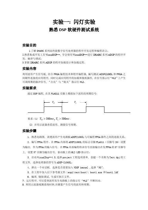
实验一: 闪灯实验熟悉DSP 软硬件测试系统实验目的1.了解SHARC 系列高性能数字信号处理器的程序开发过程和编程语言;2.熟悉集成开发工具VisualDSP++, 学会使用VisualDSP++进行SHARC 系列ADSP 的程序开发、编译与调试;3.掌握SHARC 系列ADSP 的程序加载设计和加载过程。
实验内容利用波形产生信号板, 结合FPGA 编程技术和程序编程器, 编写测试ADSP21065L 和FPGA 之间硬件连接的应用程序, 同时完成应用程序的加载和脱机操作, 在信号指示灯“HL2”上产生可调周期的脉冲信号, “点亮”与“熄灭”指示灯HL2。
实验要求通过DSP 编程, 在其FLAG11引脚上模拟如下波形的周期信号:要求:(1) 500H T ms >,500L T ms >. (2) 并用示波器查看波形, 测量信号周期。
实验步骤1. 熟悉电路图, 清楚波形产生电路板ADSP21065L 与可编程FPGA 器件之间的连接关系;2. 编写FPGA 程序。
在FPGA 内部将ADSP21065L 的标志引脚FLAG11(引脚号26)设置为输出, 作为FPGA 的输入信号, 在FPGA 内部编程将该信号直接输出在发FPGA 的37引脚号上, 设置37引脚为输出信号, 驱动板上的HL2 LED 指示灯;3. 启动VisualDsp++4.5,选择project 工程选项菜单, 创建一个名称为Test.dpj 的工程文件, 选择处理器的型号为ADSP-21065L ;4.弹出一个对话框, 选择是否需要加入VDSP kernel ,选择“NO ”;5. 在工程中加入以下参考源文件:\exp1\test(boot)\ boot1.asm 和boot1.ldf 6.编译, 链接调试, 生成可执行文件。
7.运行程序, 可以看到波形发生电路板上的指示灯“HL2”不断闪动。
8. 利用示波器观测系统时钟,并测量产生信号的波形和周期。
DSP公司各主流芯片比较

DSP公司各主流芯片比较引言DSP芯片也称数字信号处理器,是一种专门适合于进行数字信号处理运算的微处理器具,其主机应用是实时快速地实现各种数字信号处理算法。
依照数字信号处理的要求,DSP芯片一样具有如下要紧特点:〔1〕在一个指令周期内可完成一次乘法和一次加法;〔2〕程序和数据空间分开,能够同时访问指令和数据;〔3〕片内具有快速RAM,通常可通过独立的数据总线在两块中同时访问;〔4〕具有低开销或无开销循环及跳转的硬件支持;〔5〕快速的中断处理和硬件I/O支持;〔6〕具有在单周期内操作的多个硬件地址产生器;〔7〕能够并行执行多个操作;〔8〕支持流水线操作,使取指、译码和执行等操作能够重叠执行。
在我们设计DSP应用系统时,DSP芯片选型是专门重要的一个环节。
在DSP系统硬件设计中只有选定了DSP芯片,才能进一步设计其外围电路及系统的其他电路。
因此说,DSP芯片的选择应依照顾用系统的实际需要而确定,做到既能满足使用要求,又不白费资源,从而也达到成本最小化的目的。
DSP实时系统设计和开发流程如图1所示。
要紧DSP芯片厂商及其产品德州仪器公司众所周知,美国德州仪器〔Texas Instruments,TI〕是世界上最知名的DSP芯片生产厂商,其产品应用也最广泛,TI公司生产的TMS320系列DSP芯片广泛应用于各个领域。
TI公司在1982年成功推出了其第一代DSP芯片TMS32020,这是DSP应用历史上的一个里程碑,从此,DSP 芯片开始得到真正的广泛应用。
由于TMS320系列DSP芯片具有价格低廉、简单易用、功能强大等特点,因此逐步成为目前最有阻碍、最为成功的DSP系列处理器。
目前,TI公司在市场上要紧有三大系列产品:〔1〕面向数字操纵、运动操纵的TMS320C2000系列,要紧包括TMS320C24x/F24x、TMS320LC240x/LF240x、TMS320C24xA/LF240xA、TMS320C28xx等。
基于ADSP2111的数字滤波器的设计

基于ADSP2111的数字滤波器的设计第19卷第6期2004年12月内蒙古民族大学(自然科学版)Journ~ofInnerMongoliaUniversityforNationalitiesVl0L19No.6Dec.20o4基于ADSP2111的数字滤波器的设计张大伟,解乐明2(1.哈尔滨理工大学测控技术与仪器系,黑龙江哈尔滨150040;2.通辽热电厂生技部,内蒙古通辽028000)摘要:文章介绍了AnalogDevices公司)sP2l11芯片的特点,并给出了基于该芯片设计的数字滤波器,最后完成了该数字滤波器的实现.关键词:ADSP;数字滤波器;DSP中图分类号:TN911.72文献标识码:A文章编号:1671—0185(2004)06—0640—02 DesignofDigitalFilterORADSP2111ZHANGDa—wei,XIELe—min(1.DepartmentofTechnologyandInstrumentofMeasurementandControl, HarbinUniversityofScienceandTechnology,Harbin150040China;2.TongliaoThermalPowerPlant,Tongliao028000,China)Abstract:Inthispaper,featureofADSP2111ofAnalogDevicesisintroducedsimply.Andthe nsomefunctionsofdigitalfilter82"8given.FinallydesignofdigitalfilteronADSP2111iscom plet-ed.Somefunctionchartandprogram82"8alsogiven.Keywords:ADSP;Digitalfilter;DSPDSP(DigitalSignalProccessing)芯片也称数字信号处理器,是一种特别适合进行数字信号处理运算的微处理器,其主要特点是能够实时快速地实现各种数字信号处理算法.自1980年以来,DSP芯片得到了突飞猛进的发展,现在DSP芯片的应用也越来越广泛.美国模拟器件公司(Ar~ogDevices)是设计和制造DSP芯片的主要厂商之一.近年来,该公司相继推出了一系列具有自己特色的DSP芯片.文章将介绍一种数字滤波器,在其定点型DSP芯片ADSP2111的设计及应用.1AⅨ111芯片特点)sP2111可与单字节宽EPROM直接接口,能有效地引导加载程序而无需附加任何部件.被引导的存储空间由一个外部64×8位的空间组成,它分为8页(8k×8位).复位时,零引导页被自动传到ADSP2111的内部RAM中.它的串行口能以该处理器的速度全速操作,其发送字和接收字的宽度可设为3到16的任意数值.串行口还允许自动缓冲,在规定好缓冲区长度,缓冲区首地址和修改值后,它便能自动更新地址.当每个字通过串行口被传送时,数据被自动读出或写入寄存器,而无需产生中断.另外,)sP2l11还具有如下特点:2.1每个串行口具有独立的发送和接收硬件采用双缓冲寄存器,可在一个时钟周期内同时完成压扩,从而实现全双工.肛律和A律压扩功能可任意选择.2.2接口灵活每个串行口均工作在自己的串行口时钟SCLK下,SCLK和帧同步信号既可由外部输入,也可内部产生.数据字长在3--16bit之间可变.2.3使用独立的收,发帧信号定义串行数据字的传输开始可选择需不需要帧同步,长帧还是短帧,电平触发还是边沿触发.2.4自动缓冲功能当设定为自动缓冲模式后,串行口会自动接收或发送一整块的数据,不需要软件开销,仅当缓冲区的收稿日期:2004一o7一o8作者简介:张大伟(1981一),男,吉林双辽人,在读硕士研究生,主要研究仪器仪表研制与开发第6期张大伟等:基于ADSP2111的数字滤波器的设计641指针产生回绕时产生一个中断请求.2.5多路能力SPORT0具有多路选择接收和发送功能,可从24或32路时分复用比特流中选取某时隙的有效数据字.每个串行口各有五条引线与外围电路连接.分别为SCLK(时钟),(接收帧同步),1](发送帧同步),DR(数据接收)和亡rr(数据发送).3数学模型的建立和算法的实现为实现对某特定频率的滤波,程序中共使用了两种数学模型(采用的是ADSP2111定点处理器).3.1谐振器合成滤波器对某特定频率进行滤波的谐振器合成滤波器是利用对前两个数据和当前数据的相关性来实现的.这在算法实现上要比以往的FIR,IIR等传统滤波器容易得多,其主要优点是节省指令.Y a的取得与前N个数据相关,其表达式为:Y a=X(n)一RNX(n—N);Yb与前n一2个数据相关,其表达式为:Yb=Y a(n)一RY a(n一2);对于Yn的获得则通过一个谐振器对Yb进行处理,其处理算式为:Yn=∑Yb(n)+Yc(n一1)×2cos(2kn/N)一RYc(n一2)其中N值取决于所要求的带宽和采样频率.由于处理的是PCM脉码信号,故取采样频率f0=8kc,根据实际情况,建议取带宽为50Hz为佳.则有:N=/ZXf=8kc/25=320关于系数R的取值,可取经验值0.99.然后将R和COS的乘积作成一个固定系数.对应于700,900,1100,1300,1500,1700六个基准频率的值分别为0X6GOC,0X605C,0X524C,0X4236,0X327E,0X1D95.采用ADSP汇编语言来实现这一设计的程序如下:mx0=dm(i3,m0);ITLr~mx0×my0(Ss);my0=dm(const—r);mx0=dm(~2,m2);ITII-~---mx0×my0(Ss);my0=prn(i5,mS);ar=ay0一mrl;af=ay0一rnrl;ay0:at;{Yb}ITLr~mx0×my0(Ss);cntr=6;ar=mrl+af;{Yn}doresultuntilce;dm(i2,m1)=mx0;mx0=dm(~2,m1);r~ult:dm(~2,m1)=at;my0=din(const—r2);3.2水缸判别对滤波器滤出的数据进行水缸积累,使之达到一种动态平衡,让其在有数据时水缸渐满,无数据时水缸不变.这时有:A=YcIM+A—AIM.其中M的取值取决于所要计算的数据的多少,本程序中取M=128.用ADSP汇编语言可以实现这一设计,程序略.4结语随着信息技术的深入和计算机技术的飞速发展,数字信号处理技术已经发展成为--tq关键的技术学科.而数字滤波作为数字信号处理的一个基本的学科分支,也得到了越来越广泛的应用.文章介绍ADSP2111实现的数字滤波器,对某些特定频率的滤波可根据需要十分方便地通过修改其参数来加以修改,而且DSP实现的数字滤波器除具有精确度高,稳定好等特点外,还具有灵活性好,不受环境影响等优点.在实际工作中,具有比较高的实用价值.参考文献[1]陈峰.Blacldin系列DSP原理与系统设计[M].北京:电子工业出版社,2004.[2]吴敏渊.ADSP系列数字信号处理器原aiM].北京:电子工业出版社,2002.[3]赵建芬,谭玉波,程少龙,等.ADSP系列数字信号处理器件的应用[J].国外电子元器件,2001,(1):57—60(责任编辑包金山]。
ADSP-21262型DSP的监控设计(精)

ADSP-21262型DSP的监控设计1 引言随着数字信号处理理论的日趋完善和超大规模集成电路技术的飞速发展,在各种实时处理应用需求的推动下,数字信号处理器(DSP)也得到了越来越广泛的应用。
DSP的监控是DSP开发和应用中十分重要的环节。
目前在DSP的开发过程中,最常用的方式是通过购买处理器的JTAG仿真器和开发软件包实现对DSP的调试和监控。
JTAG调试工具的功能十分强大,对于不熟悉DSP内部结构和细节的开发者而言是一种非常不错的选择。
但是此种方法也有其缺陷:首先,开发成本比较昂贵,一般购买正版仿真器和软件包的价格都在数千美元至数万美元不等;其次,通用性不强。
不但不同公司的处理器需要使用不同的仿真器,同一公司的不同系列DSP之间也没有兼容性。
基于以上原因,笔者结合ADSP-21262的开发研究了其他的监控实现方式。
2 单DSP系统监控设计2.1 ADSP-21262简介ADSP-21262是ADI公司推出的一款高性能浮点数字信号处理器,特性如下:200 MHz工作主频。
1 200 MFLOPS;超级哈佛结构,内部三条独立总线,三级流水线结构;2 Mbit双口SRAM,4 Mbit双口ROM;双内核结构,支持SISD和SIMD工作模式;22条独立的DMA通道;丰富的外围设备接口。
2.2 单DSP系统监控硬件设计单ADSP-21262型DSP系统的监控部分硬件电路如图1所示。
ADSP-21262支持多种上电引导方式,如外部EPROM引导、SPI主模式引导、SPI从模式引导。
这里选取SPI主模式作为其引导方式。
AT25F1024为串行SPI Flash存储器,用于存储ADSP-21262需要引导的程序。
如果这里存储的是监控程序,则DSP完成上电引导后便可进入监控状态。
并能执行相应的监控功能操作。
这里用异步串口(UART)作为监控系统与用户PC机的通讯接口,完成底层监控程序和PC端监控服务软件之间的通讯。
基于ADS的声表滤波器匹配电路设计分析

基于ADS的声表滤波器匹配电路设计分析摘要:为进一步提高声表滤波器装置在射频电路实际使用中的性能,不仅要对声表滤波器装置本身进行性能优化处理,同时,其他部分的外部电路同样十分重要,需要保证阻抗匹配可以达到标准水平。
本文以上述内容为核心,针对声表滤波器装置实际使用性能的发挥展开研究,分析在射频电路中的具体应用情况,总结相关经验并归纳出部分常用声表滤波器装置在常规射频电路中的常见阻抗匹配方式,同时也给出两种新的在射频电路中不平衡转平衡状态下的阻抗匹配设定建议,并对二者进行ADS仿真测试,经仿真测试分析后,可证明这两种方法可以有效提升滤波器装置在电路中的使用性能,进而为整个电路提供良好的性能优化保障作用。
关键词:射频电路;声表滤波器;阻抗匹配;ADS前言:新时期背景下,现有移动通信技术领域的发展速度不断加快,声表滤波器装置的应用范围也在不断扩展,在系统应用程度不断加深的情况下,声表滤波器装置的实际使用性能也在面临着更高级别的要求。
但是,关于射频电路实际运行中的应用,还需要对使用性能做出充分考量,为此,设计者一般会将声表滤波器装置设计成多种不同的形式,所以,可将声表滤波器装置视为一个单独的网络,与其相对应的则是输入与输出两个不同端口,在将其应用到实际电路中以后,声表滤波器装置便需要与外部其他电路进行直接连接和阻抗匹配,通过这种方式保证电路使用性能可以达到期望水平。
1 声表滤波器概述目前,声表面波(SAW)滤波器装置在2G接收机设备的前端或者双工器设备和接收滤波器设备中的应用十分常见。
其中,SAW滤波器装置自身具有低插入损耗优势和突出的抑制性能,在实际使用过程中不仅能够达到带宽标准,同时其自身体积与传统类型的腔体结构或者陶瓷滤波器装置对比更小,具有突出优势。
因此,SAW滤波器可以被布设在晶圆上,在这样的条件下,能够有效降低成本,并执行批量生产[1]。
此外,SAW技术还能够支持各种不同频段的专业滤波器或者双工器进行整合处理,布设在单一芯片内,这样的布设优势仅需少量或者根本不需其他的额外工艺即可实现设计目标,在保证使用效果的前提下,具有量多使用优势。
- 1、下载文档前请自行甄别文档内容的完整性,平台不提供额外的编辑、内容补充、找答案等附加服务。
- 2、"仅部分预览"的文档,不可在线预览部分如存在完整性等问题,可反馈申请退款(可完整预览的文档不适用该条件!)。
- 3、如文档侵犯您的权益,请联系客服反馈,我们会尽快为您处理(人工客服工作时间:9:00-18:30)。
引言
随着数字信号处理理论的日趋完善和超大规模集成电路技术的飞速发展,在各种实时处理应用需求的推动下,数字信号处理器(DSP)也得到了越来越广泛的应用。
DSP的监控是DSP开发和应用中十分重要的环节。
目前在DSP的开发过程中,最常用的方式是通过购买处理器的JTAG仿真器和开发软件包实现对DSP的调试和监控。
JTAG调试工具的功能十分强大,对于不熟悉DSP内部结构和细节的开发者而言是一种非常不错的选择。
但是此种方法也有其缺陷:首先,开发成本比较昂贵,一般购买正版仿真器和软件包的价格都在数千美元至数万美元不等;其次,通用性不强。
不但不同公司的处理器需要使用不同的仿真器,同一公司的不同系列DSP之间也没有兼容性。
基于以上原因,笔者结合ADSP-21262的开发研究了其他的监控实现方式。
2 单DSP系统监控设计
2.1 ADSP-21262简介
ADSP-21262是ADI公司推出的一款高性能浮点数字信号处理器,特性如下:
200MHz工作主频。
1200MFLOPS;
超级哈佛结构,内部三条独立总线,三级流水线结构;
2Mbit双口SRAM,4Mbit双口ROM;
双内核结构,支持SISD和SIMD工作模式;
22条独立的DMA通道;
丰富的外围设备接口。
2.2 单DSP系统监控硬件设计
单ADSP-21262型DSP系统的监控部分硬件电路如图1所示。
ADSP-21262支持多种上电引导方式,如外部EPROM引导、SPI主模式引导、SPI从模式引导。
这里选取SPI主模式作为其引导方式。
AT25F1024为串行SPIFlash存储器,用于存储ADSP-21262需要引导的程序。
如果这里存储的是监控程序,则DSP完成上电引导后便可进入监控状态。
并能执行相应的监控功能操作。
这里用异步串口(UART)作为监控系统与用户 PC机的通讯接口,完成底层监控程序和PC端监控服务软件之间的通讯。
MAX232为电平转换器件,将DSP端的CMOS电平转化为PC端的RS232电平。
大多数DSP均不提供自带的UART接口,但是由于UART接口为大多数工程人员所熟悉。
并且连线简单,很容易通过两根通用I/O口来分别模拟其 Tx、Rx信号,故这里采用此方案。
当然也可以用USB控制器或网口控制器实现USB 接口方式或网络接口方式的监控。
无论是PC机层的监控服务软件设计,还是底层的监控功能程序设计,在原理上基本一致,不同的只是上层PC机的监控服务软件和底层DSP的监控功能程序之间的通讯所采用的接口方式。
这里以UART接口的监控系统为例进行详细介绍。
2.3 监控软件设计
监控的主要功能是方便DSP的调试,故其应该为用户提供的功能主要包括:
处理器的复位和初始化;
程序的装载和运行;
查看DSP内部数据区和程序区;
写DSP内部数据区和程序区;
查看相关的系统寄存器;
程序代码的反汇编显示。
监控软件的设计由上层PC机监控服务软件和底层DSP监控功能程序两部分组成,它的层次结构如图2所示。
2.3.1 PC机软件设计
PC机软件是用户实现DSP监控操作的平台,由C++Builder5.0开发完成。
主要由监控软件界面、各个监控功能模块和UART驱动函数模块组成。
监控软件界面是监控系统和用户进行信息交互的平台,它整合了各个监控功能模块,用户通过它完成各个功能模块的调用、参数的传递、结果的显示等。
PC监控功能模块完成对底层DSP监控功能程序的调用,从而实现用户所需的相应监控功能。
UART驱动函数模块的作用是实现上层PC机的监控服务软件和底层DSP的监控功能程序之间的UART接口通讯。
2.3.2 底层软件设计
底层DSP监控功能程序是整个监控功能实现的核心,由汇编语言开发完成。
它由底层监控功能模块和UART协议收发驱动函数模块组成。
底层监控功能模块可以供PC端监控功能模块进行调用,它直接负责完成对DSP的相应管理和操作,如:程序的装载和运行、DSP内部指定地址存储区的读写、寄存器的读写等。
由于ADSP-21262不带UART接口,于是需要UART协议收发驱动函数用两个通用I/O引脚模拟UART的工作时序,以实现DSP与PC间的通讯。
2.4 单DSP系统监控的工作机制
系统的监控功能需要PC机软件和底层软件协同工作来实现,工作流程如图3所示。
图3中左半部分代表底层DSP监控功能程序的流程,右半部分代表PC机监控服务软件的操作流程,中间的虚线代表底层软件和PC机软件之间有数据通讯。
ADSP-21262内有1Mbit的程序存储器 (PM),当配置为32位字长时,其地址空间为:0X80000~0X87FFF。
其中0X80000~0X800FF为中断向量表的位置,其后的空间被分为两部分,分别存放用户程序和监控程序。
其中用户程序驻留在低地址空间,监控程序驻留在高地址空间,具体位置用户可以根据监控程序的大小作出调整。
DSP的程序区示意图如图4所示。
底层监控程序中UART的模拟是通过定时对Rx和Tx信号线进行采样来实现的,因此在监控程序中断向量表中的定时中断 _TMZHI处执行JUMPTIMER0_INT指令,其中TIMER0_INT处为定时中断服务程序,用于实现UART的收发功能。
而在下载用户程序时,监控程序的中段向量表被用户的中断向量表所覆盖,于是就无法执行相应的UART操作了,为了解决该问题,在监控程序中加入以下代码段:
其作用就是保护定时中断向量入口,以保证正确进入定时中断服务程序。
3 多DSP系统监控设计
3.1 多DSP系统监控硬件设计
多ADSP-21262的DSP系统监控电路如图5所示。
此系统共由5个ADSP-21262组成。
其中DSP0被设为主处理器,其余4个作为从处理器。
主处理器可以通过SPI总线与各从处理器通讯。
从而实现对各从处理器的监控操作。
而PC机与主处理器之间则采用上文所述的单DSP系统的监控方式,这里不作赘述。
主DSP设置为EPROM引导方式,上电后从外部 EPROM中引导其监控程序PROGRAM_A。
各从DSP则设置为SPI从引导方式,等待主DSP完成其自身引导后,再将监控程序PROGRAM_B通过SPI口写入从DSP中。
完成引导后主/从DSP分别进入各自的监控状态。
3.2 多DSP系统监控工作机制
此系统中,PC机对主DSP的监控机制与单DSP系统相似,但是PC机监控软件向主DSP发送监控命令时,在命令字节中添加了DSP的ID信息,ID0~ID4分别对应DSP0~DSP4。
主DSP接收到命令字节后提取出其中的ID信息,判断
用户所期望的DSP代码,如果是对主DSP自身的监控命令,则按照单DSP系统的监控机制进行操作;如果是对某一从 DSP的监控命令,则主DSP选中相应的从DSP,并通过SPI口将监控命令发往相应的从DSP,从DSP在执行完用户所要求的监控功能后将结果通过 SPI口发往主DSP,再由主DSP发送给PC机监控服务软件。
从而实现用户对系统中各DSP的灵活管理。
对于不带SPI接口的DSP,也完全可以采用其他各种通讯接口作为主DSP与从DSP之间的接口。
4 结束语
本文探讨和研究了ADI公司SHARC系列DSPADSP-21262的监控原理和实现机制。
并以单DSP和多DSP系统为例,分别详细介绍了以UART口作为监控接口的监控设计方法。
此方法也完全适用于其他各类DSP的监控实现。
用户可以根据系统需要和DSP所能提供的资源采用其他的监控方法:例如PC与主DSP之间的监控接口可以选择为USB口、网口等;而主DSP与从DSP之间的通讯也能通过其他各类总线,例如并行的数据/地址总线、同步串口、I2C、HPI、LINK等,完全取决于用户的需要,十分灵活方便。