BAV99BRW-7-F;中文规格书,Datasheet资料
BAW56双面切换二极管数据手册说明书
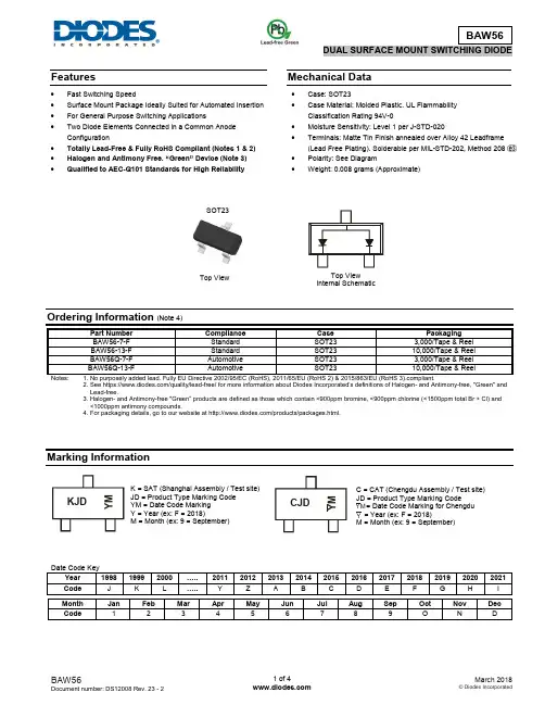
Features∙ Fast Switching Speed∙ Surface Mount Package Ideally Suited for Automated Insertion ∙ For General Purpose Switching Applications∙ Two Diode Elements Connected in a Common Anode Configuration∙ Totally Lead-Free & Fully RoHS Compliant (Notes 1 & 2) ∙ Halogen and Antimony Free. “Green” Device (Note 3) ∙ Qualified to AEC-Q101 Standards for High ReliabilityMechanical Data∙ Case: SOT23∙ Case Material: Molded Plastic. UL Flammability Classification Rating 94V-0∙ Moisture Sensitivity: Level 1 per J-STD-020∙ Terminals: Matte Tin Finish annealed over Alloy 42 Leadframe (Lead Free Plating). Solderable per MIL-STD-202, Method 208 ∙ Polarity: See Diagram∙Weight: 0.008 grams (Approximate)Ordering Information (Note 4)2. See https:///quality/lead-free/ for more information about Diodes Incorporated’s definitions of Halogen - and Antimony-free, "Green" and Lead-free.3. Halogen- and Antimony-free "Green” products are defined as those which contain <900ppm bromine, <900ppm chlorine (<1500ppm total Br + Cl) and <1000ppm antimony compounds.4. For packaging details, go to our website at /products/packages.html.Marking InformationTop ViewSOT23Top ViewInternal SchematicK = SAT (Shanghai Assembly / Test site) JD = Product Type Marking Code YM = Date Code Marking Y = Year (ex: F = 2018)M = Month (ex: 9 = September) C = CAT (Chengdu Assembly / Test site)JD = Product Type Marking Code= Date Code Marking for Chengdu = Year (ex: F = 2018) M = Month (ex: 9 = September)CJDY MKJD Y MYMY(@T = +25°C, unless otherwise specified.)Thermal CharacteristicsNotes: 5. Part mounted on FR-4 substrate PC board with 1inch squared, 2oz copper pad layout.6. Short duration pulse test used to minimize self-heating effect.400T , AMBIENT TEMPERATURE, (°C)Fig. 1 Power Derating Curve, Total Package A P P O W E R D I S S I P A T I O N (m W )D ,1000.110.010.001I , I N S T A N T A N E O U S F O R W A R D C U R R E N T (A )F V , INSTANTANEOUS FORWARD VOLTAGE (V)Fig. 2 Typical Forward Characteristics, Per Element F0.11101001,00010,000V , INSTANTANEOUS REVERSE VOLTAGE (V)Fig. 3 Typical Reverse Characteristics, Per Element R I , I N S T A N T A N E O U S R E V E R S E C U R R E N T (n A )R 0.00.20.40.60.81.81.61.41.21.02.0010204030C , T O T A L C A P A C I T A N C E (p F )T V , DC REVERSE VOLTAGE (V)Fig. 4 Total Capacitance vs. Reverse Voltage, Per Element RPackage Outline DimensionsPlease see /package-outlines.html for the latest version.Suggested Pad LayoutPlease see /package-outlines.html for the latest version.SOT23。
BAV99中文资料
1999 May 11
4
元器件交易网
Philips Semiconductors
High-speed double diode
Product specification
BAV99
105
IR (nA)
104
VR = 75 V
103 max
75 V
MGA884
102
25 V
typ
元器件交易网
DISCRETE SEMICONDUCTORS
DATA SHEET
book, halfpage
M3D088
BAV99 High-speed double diode
Product specification Supersedes data of 1996 Sep 17
t = 1 µs t = 1 ms t=1s Tamb = 25 °C; note 1
Note 1. Device mounted on an FR4 printed-circuit board.
MIN.
− − −
−
−
− − − − −65 −
MAX.
85 75 215
125
450
4 1 0.5 250 +150 150
max. 75 V • Repetitive peak reverse voltage:
max. 85 V • Repetitive peak forward current:
max. 450 mA.
APPLICATIONS
• High-speed switching in thick and thin-film circuits.
DESCRIPTION
TBAV99,LM(T高速开关二极管
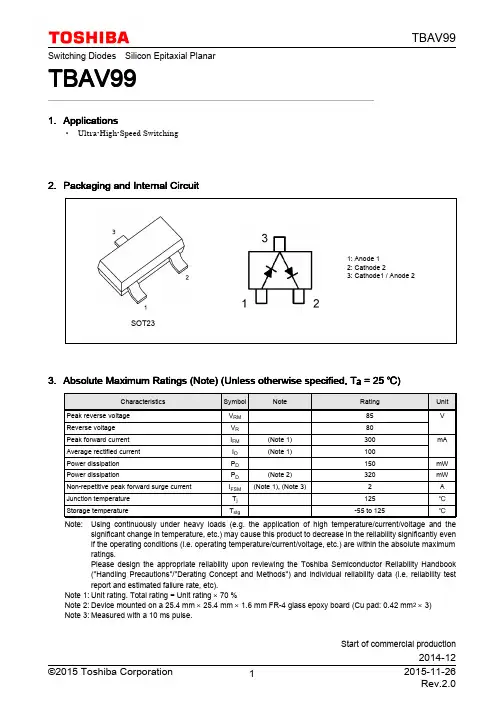
TBAV99
Switching Diodes Silicon Epitaxial Planar
TBAV99
1. Applications
• Ultra-High-Speed Switching
2. Packaging and Internal Circuit
1: Anode 1 2: Cathode 2 3: Cathode1 / Anode 2
SOT23
3. Absolute Maximum Ratings (Note) (Unless otherwise specified, Ta = 25 )
Characteristics Peak reverse voltage Reverse voltage Peak forward current Average rectified current Power dissipation Power dissipation Non-repetitive peak forward surge current Junction temperature Storage temperature Symbol VRM VR IFM IO PD PD IFSM Tj Tstg (Note 2) (Note 1), (Note 3) (Note 1) (Note 1) Note Rating 85 80 300 100 150 320 2 125 -55 to 125 mW mW A mA Unit V
Bav99 Bav99W快速开关二极管参数
Power Dissipation功耗
Pd
BAV99W
200
mW
BAV99
350
Typical Thermal Resistance, Junction to Ambient Air典型的热电阻,结对环境空气
RθJA
BAV99W
625
K/W
BAV99
357
Operating and Storage Temperature Range操作和储存温度范围
Bav99 Bav99W快速开关二极管参数
来源:|时间:2010年05月02日
表面贴装快速开关二极管:BAV99 BAV99W
最大额定值:
Characteristic参数
符号
数值
单位
Non-Repetitive Peak Reverse Voltage非重复峰值反向电压
VRM
100
V
Peak Repetitive Reverse Voltage Working Peak Reverse Voltage DC Blocking Voltage峰值重复反向电压峰值反向工作电压直流阻断电压
VRRMHale Waihona Puke VRWM VR75V
Forward Continuous Current正向连续电流
IF
300
mA
Average Rectified Output Current平均整流输出电流
IO
150
mA
Peak Forward Surge Current @t<1.0μs峰值正向浪涌电流
IFSM
2.0
Tj, TSTG
-65 to +150
BAV99BRW-7-F;中文规格书,Datasheet资料
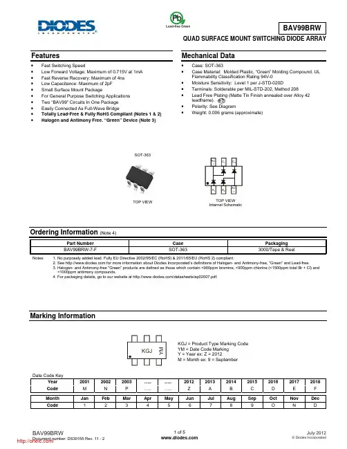
QUAD SURFACE MOUNT SWITCHING DIODE ARRAYFeatures• Fast Switching Speed• Low Forward Voltage: Maximum of 0.715V at 1mA • Fast Reverse Recovery: Maximum of 4ns • Low Capacitance: Maximum of 2pF • Small Surface Mount Package• For General Purpose Switching Applications • Two “BAV99” Circuits In One Package • Easily Connected As Full-Wave Bridge• Totally Lead-Free & Fully RoHS Compliant (Notes 1 & 2) • Halogen and Antimony Free. “Green” Device (Note 3)Mechanical Data• Case: SOT-363 • Case Material: Molded Plastic, “Green” Molding Compound. ULFlammability Classification Rating 94V-0 • Moisture Sensitivity: Level 1 per J-STD-020D • Terminals: Solderable per MIL-STD-202, Method 208 • Lead Free Plating (Matte Tin Finish annealed over Alloy 42leadframe).• Polarity: See Diagram •Weight: 0.006 grams (approximate)Ordering Information (Note 4)Part Number Case Packaging BAV99BRW-7-FSOT-363 3000/Tape & ReelNotes: 1. No purposely added lead. Fully EU Directive 2002/95/EC (RoHS) & 2011/65/EU (RoHS 2) compliant.2. See for more information about Diodes Incorporated’s definitions of Halogen- and Antimony-free, "Green" and Lead-free.3. Halogen- and Antimony-free "Green” products are defined as those which contain <900ppm bromine, <900ppm chlorine (<1500ppm total Br + Cl) and <1000ppm antimony compounds.4. For packaging details, go to our website at /datasheets/ap02007.pdf.Marking InformationDate Code KeyYear 2001 2002 2003 ….. ….. 2012 2013 2014 2015 2016 2017 2018 CodeM N P ….. ….. Z A B C D E FMonth JanFebMarAprMayJunJulAugSepOctNovDecCode1 2 3 4 5 6 7 8 9 O N De3TOP VIEWSOT-363TOP VIEW Internal SchematicAC 1AC2C 1A 1C 2A 2KGJ = Product Type Marking Code YM = Date Code Marking Y = Year ex: Z = 2012M = Month ex: 9 = SeptemberKGJY MMaximum Ratings(@T A = +25°C, unless otherwise specified.)Characteristic Symbol Value Unit Non-Repetitive Peak Reverse Voltage V RM100 VPeak Repetitive Reverse Voltage Working Peak Reverse Voltage DC Blocking Voltage V RRMV RWMV R75 VRMS Reverse Voltage V R(RMS)53 V Forward Continuous Current (Note 5) I FM300 mA Average Rectified Output Current (Note 5) I O150 mANon-Repetitive Peak Forward Surge Current @ t = 1.0µs@ t = 1.0s I FSM2.01.0AThermal CharacteristicsCharacteristic Symbol Value Unit Power Dissipation (Note 5) P D200 mW Thermal Resistance Junction to Ambient Air (Note 5) RθJA625 °C/W Operating and Storage Temperature Range T J , T STG-65 to +150 °CElectrical Characteristics(@T A = +25°C, unless otherwise specified.)Characteristic Symbol Min Max Unit Test Condition Reverse Breakdown Voltage (Note 6) V(BR)R75 ⎯V I R = 2.5µAForward Voltage V F⎯0.7150.8551.01.25VI F = 1.0mAI F = 10mAI F = 50mAI F = 150mAReverse Current (Note 6) I R⎯2.5503025µAµAµAnAV R = 75VV R = 75V, T J = +150°CV R = 25V, T J = +150°CV R = 20VTotal Capacitance C T⎯ 2.0 pF V R = 0, f = 1.0MHzReverse Recovery Time t rr⎯ 4.0 ns I F = I R = 10mA,I rr = 0.1 x I R, R L = 100ΩNotes: 5. Device mounted on FR-4 PC board with recommended pad layout, which can be found on our website at /datasheets/ap02001.pdf.6. Short duration pulse test used to minimize self-heating effect.501001502002502505075100125150P , P O W E R D I S S I P A T I O N (m W )D T , AMBIENT TEMPERATURE (°C)A Figure 1 Power Derating Curve, Total Package300Note 50.10.01I , I N S T A N T A N E O U S F O R W A R D C U R R E N T (A )F V , INSTANTANEOUS FORWARD VOLTAGE (V)Figure 2 Typical Forward Characteristics, Per Element F1001,00010,000V , INSTANTANEOUS REVERSE VOLTAGE (V)Figure 3 Typical Reverse Characteristics, Per ElementR I , I N S T A N T A N E O U S R E V E R S E C U R R E N T (n A )R 0.00.20.40.60.81.81.61.41.21.02.020C , T O T A L C A P A C I T A N C E (p F )T V , DC REVERSE VOLTAGE (V)Figure 4 Total Capacitance vs. Reverse Voltage, Per ElementRPackage Outline DimensionsSuggested Pad LayoutSOT363Dim Min Max Typ A 0.100.30 0.25 B 1.15 1.35 1.30 C 2.00 2.20 2.10 D 0.65 TypF 0.400.45 0.425 H 1.80 2.20 2.15 J 0 0.10 0.05 K 0.90 1.00 1.00 L 0.250.40 0.30 M 0.100.22 0.11α0° 8° -All Dimensions in mmDimensions Value (in mm)Z 2.5 G 1.3 X 0.42 Y 0.6 C1 1.9 C2 0.65XZYC1C2C2GIMPORTANT NOTICEDIODES INCORPORATED MAKES NO WARRANTY OF ANY KIND, EXPRESS OR IMPLIED, WITH REGARDS TO THIS DOCUMENT, INCLUDING, BUT NOT LIMITED TO, THE IMPLIED WARRANTIES OF MERCHANTABILITY AND FITNESS FOR A PARTICULAR PURPOSE (AND THEIR EQUIVALENTS UNDER THE LAWS OF ANY JURISDICTION).Diodes Incorporated and its subsidiaries reserve the right to make modifications, enhancements, improvements, corrections or other changes without further notice to this document and any product described herein. Diodes Incorporated does not assume any liability arising out of the application or use of this document or any product described herein; neither does Diodes Incorporated convey any license under its patent or trademark rights, nor the rights of others. Any Customer or user of this document or products described herein in such applications shall assume all risks of such use and will agree to hold Diodes Incorporated and all the companies whose products are represented on Diodes Incorporated website, harmless against all damages.Diodes Incorporated does not warrant or accept any liability whatsoever in respect of any products purchased through unauthorized sales channel. Should Customers purchase or use Diodes Incorporated products for any unintended or unauthorized application, Customers shall indemnify and hold Diodes Incorporated and its representatives harmless against all claims, damages, expenses, and attorney fees arising out of, directly or indirectly, any claim of personal injury or death associated with such unintended or unauthorized application.Products described herein may be covered by one or more United States, international or foreign patents pending. Product names and markings noted herein may also be covered by one or more United States, international or foreign trademarks.LIFE SUPPORTDiodes Incorporated products are specifically not authorized for use as critical components in life support devices or systems without the express written approval of the Chief Executive Officer of Diodes Incorporated. As used herein:A. Life support devices or systems are devices or systems which:1. are intended to implant into the body, or2. support or sustain life and whose failure to perform when properly used in accordance with instructions for use provided in thelabeling can be reasonably expected to result in significant injury to the user.B. A critical component is any component in a life support device or system whose failure to perform can be reasonably expected to cause thefailure of the life support device or to affect its safety or effectiveness.Customers represent that they have all necessary expertise in the safety and regulatory ramifications of their life support devices or systems, and acknowledge and agree that they are solely responsible for all legal, regulatory and safety-related requirements concerning their products and any use of Diodes Incorporated products in such safety-critical, life support devices or systems, notwithstanding any devices- or systems-related information or support that may be provided by Diodes Incorporated. Further, Customers must fully indemnify Diodes Incorporated and its representatives against any damages arising out of the use of Diodes Incorporated products in such safety-critical, life support devices or systems.Copyright © 2012, Diodes Incorporated分销商库存信息: DIODESBAV99BRW-7-F。
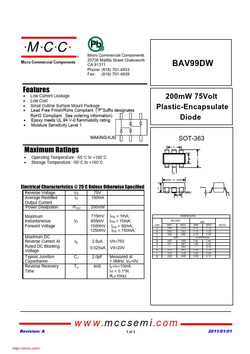
BAV99DW-TP;中文规格书,Datasheet资料
TM
Micro Commercial Components
omponents 20736 Marilla Street Chatsworth !"# $
% !"#
BAV99DW
B
A H
Electrical Characteristics @ 25°C Unless Otherwise Specified
Reverse Voltage Average Rectified Output Current Power Dissipation Maximum Instantaneous Forward Voltage Maximum DC Reverse Current At Rated DC Blocking Voltage Typical Junction Capacitance Reverse Recovery Time VR IO PTOT VF 75V 150mA 200mW 715mV IFM = 1mA; 855mV IFM = 10mA; 1000mV IFM = 50mA; 1250mV IFM = 150mA; 2.5uA 0.025uA CJ Trr 2.0pF 4nS VR=75V VR=20V Measured at 1.0MHz, VR=0V IF=IR=10mA I rr = 0.1*IR Rc=100Ω
/
3 of 3
பைடு நூலகம்
Revision: A
2011/01/01
分销商库存信息:
MICRO-COMMERICAL-CO BAV99DW-TP
K J D
M
L
DIMENSIONS
INCHES DIM A B C D G H J K L M MIN .006 .045 .085 .026 .047 .071 --.035 .010 .003 .055 .087 .004 .043 .018 .006 MAX .014 .053 .096
A7_BAV99
Ratings at 25O C ambient temperature unless otherwise specified.Single phase, half wave, 60 Hz, resistive or inductive load.For capacitive load, derate current by 20%.
SOT-23
Publication thereof does not convey nor imply any license under patent or other industrial or intellectual property rights.
PanJit Internatioal Inc.
TEL:886-7-6213121 Fax:886-7-6213129 Internet: email: sales@
a7_bav99 partnumber: bal99, baw56, bav70, bav99 page bal99,baw56, bav70, bav99 surface mount switching diodes voltage 75 volts 350 mwatts features fastswitching speed. surfacemount package ideally suited automaticinsertion electricallyidentical standardjedec highconductance mechani cal data case: sot-23, plastic terminals: solderable per mil-std-202, method 208 approx. weight: 0.008 gram marking jf,jc, ja, jg maxi mum rati ngs electrical characteri sti cs ratings ambienttemperature unless otherwise specified. single phase, half wave, 60 hz, resistive inductiveload. capacitiveload, derate current 20%.note: vr=0,f=1mhz 2.from if=10ma ir=1ma,vr=6volts, rl=100? package sot-23 power bal99single (alt) common anode baw56 common cathode bav70 series bav99 part number: bal99, baw56, bav70, bav99 page rating characteristi curvesrectification effciency measurement circuit typical capaticance leakage current forward voltage 100 0.2 0.4 0.6 0.8 1.0 1.2 10 1.0 0.10 4.53.5 1.5 forwardv
各式贴片二极管基本参数
各式贴片二极管基本参数TYPE Io(A) VR(V) VF(V) IR(μA) PD(mW) Package 1N4148W 150mA 75 1.25 1.0 350 SOD-123 1N4448W 250mA 75 1.25 2.5 350 SOD-123 BAV16W 150mA 75 1.25 1.0 400 SOD-123 BAV19W 200mA 100 1.25 0.1 250 SOD-123 BAV20W 200mA 150 1.25 0.1 250 SOD-123 BAV21W 200mA 200 1.25 0.1 250 SOD-123 1N4148WS 150mA 75 1.25 1.0 350 SOD-323 1N4448WS 250mA 75 1.25 2.5 350 SOD-323 BAV16WS 150mA 75 1.25 1.0 400 SOD-323 BAV19WS 200mA 100 1.25 0.1 250 SOD-323 BAV20WS 200mA 150 1.25 0.1 250 SOD-323 BAV21WS 200mA 200 1.25 0.1 250 SOD-323 1SS387 100mA 80 1.2 0.5 150 SOD-523 1SS388 100mA 40 0.6 5.0 150 SOD-523 1SS400 100mA 90 1.2 0.1 150 SOD-523 1SS422 150mA 85 1.2 0.1 150 SOD-523 BAS16X 150mA 75 1.25 1.0 150 SOD-523 BAS516 200mA 75 1.25 1.0 200 SOD-523 1SS400G 100mA 90 1.2 0.1 100 SOD-723 TYPE Io(A) VR(V) VF(V) IR(μA) Trr(nS) Package BAT42W - 30 0.65 0.2 - SOD-123 BAT43W - 30 0.45 0.2 - SOD-123 BAT46W - 30 0.45 0.2 - SOD-123 SD101AW - 60 1.0 0.2 - SOD-123 SD101BW - 50 0.95 0.2 - SOD-123 SD101CW - 40 0.9 0.2 - SOD-123 1N5711W - 70 1.0 0.2 - SOD-123 1N6263W - 60 1.0 0.2 - SOD-123 B0520W 0.5 20 0.385 250 - SOD-123 B0530W 0.5 30 0.43 130 - SOD-123 B0540W 0.5 40 0.62 20 - SOD-123 B5817W 1.0 20 0.75 1000 - SOD-123 B5819W 1.0 40 0.9 1000 - SOD-123 FM120-M-FM1100-M 1.0 20-100 0.5-0.85 1000 - SOD-123 FM220-M-FM2100-M 2.0 20-100 0.5-0.85 1000 - SOD-123 BAT42WS - 30 0.65 0.5 - SOD-323 BAT43WS - 30 0.45 0.5 - SOD-323 BAT54WS - 30 1.0 2.0 - SOD-323BAS40WS - 40 1.0 0.2 - SOD-323 BAS70WS - 70 1.0 0.1 - SOD-323 SD101AWS - 60 1.0 0.2 - SOD-323 SD101BWS - 50 0.95 0.2 - SOD-323 SD101CWS - 40 0.9 0.2 - SOD-323 SD103AWS - 40 0.37 5.0 - SOD-323 SD103BWS - 30 0.6 5.0 - SOD-323 SD103CWS - 20 0.6 5.0 - SOD-323 MBR0520WS - 20 0.31 0.1 - SOD-323 MBR0530WS - 30 0.36 0.03 - SOD-323 MBR0540WS - 40 0.36 0.03 - SOD-323 1N5711WS - 70 1.0 0.2 - SOD-323 BAT54X 200mA 30 0.8 2.0 - SOD-523 RB520S-30 200mA 30 0.45 0.5 - SOD-523 RB521S-30 200mA 30 0.35 10 - SOD-523 RB751S-40 30mA 40 0.37 0.5 - SOD-523 RB520G-30 100mA 30 0.345 0.5 - SOD-723 RB521G-30 100mA 30 0.35 10 - SOD-723 RB751G-40 30mA 40 0.37 0.5 - SOD-723 FM4001-M-FM4007-M 1.0 50-1000 1.10 5.0 - SOD-123 FFM-101-M-FFM107-M 1.0 50-1000 1.3 5.0 150-500 SOD-123 MURX0505-MURX0560 0.5 50-600 1.35 5.0 75 SOD-123 HFM101-M-HFM107-M 1.0 50-1000 1.0-1.7 5.0 50-75 SOD-123 BB910 a a a a a SOD-123 BZT52C2V4-BZT52C51 1/2W a a a a SOD-123 BZT52C2V0S-BZT52C39S 1/4W a a a a SOD-323 TYPE Io(A) VR(V) VF(V) IR(μA) PD(mW) Package 1SS181 - 80 1.2 0.5 150 SOT-23 1SS184 - 80 1.2 0.5 150 SOT-23 1SS187 - 80 1.2 0.5 150 SOT-23 1SS190 - 80 1.2 0.5 150 SOT-23 1SS193 - 80 1.2 0.5 150 SOT-23 1SS196 - 80 1.2 0.5 150 SOT-23 1SS226 - 80 1.2 0.5 150 SOT-23 BAL99LT1 - 70 1.25 2.5 350 SOT-23 BAS116LT1 - 75 1.25 5.0 300 SOT-23 BAS16LT1 - 75 1.25 1.0 225 SOT-23 BAS19LT1 - 120 1.25 0.1 225 SOT-23 BAS21LT1 - 250 1.25 1.0 225 SOT-23 BAV70LT1 - 70 1.0 5.0 350 SOT-23BAW56LT1 - 70 1.0 2.5 350 SOT-23 BAV74LT1 - 50 1.0 0.1 225 SOT-23 BAV99LT1 - 70 1.25 2.5 225 SOT-23 DAN202K - 70 1.25 2.5 225 SOT-23 DAP202K - 70 1.25 2.5 225 SOT-23 MA147 - 80 1.2 100 - SOT-23 MA153 - 40 1.2 0.1 - SOT-23 MA153A - 80 1.2 0.1 - SOT-23 MA157A - 80 1.2 0.1 - SOT-23 MMBD914LT1 - 75 1.25 2.5 225 SOT-23 MMBD2836LT1 - 75 1.0 0.1 225 SOT-23 MMBD2838LT1 - 75 1.2 0.1 225 SOT-23 MMBD6050LT1 - 70 1.1 0.1 225 SOT-23 MMBD7000LT1 - 100 1.1 5.0 225 SOT-23 SDS7000 - 100 1.1 5.0 225 SOT-23 BAS16W - 75 1.25 1.0 200 SOT-323 BAS19W - 100 1.25 0.1 200 SOT-323 BAS20W - 150 1.25 0.1 200 SOT-323 BAS21W - 200 1.25 0.1 200 SOT-323 BAV70W - 75 1.25 2.5 200 SOT-323 BAV99W - 75 1.25 2.5 200 SOT-323 BAW56W - 75 1.25 2.5 200 SOT-323 MMBD4148W - 75 1.25 1.0 200 SOT-323 MMBD4448W - 75 1.25 2.5 200 SOT-323 BAS16T - 85 1.25 2.0 150 SOT-523 BAW56T - 85 1.25 2.0 150 SOT-523 BAV70T - 85 1.25 2.0 150 SOT-523 BAV99T - 85 1.0 2.0 150 SOT-523 DAN222 - 80 1.2 0.1 100 SOT-523 DAP222 - 80 1.2 0.1 100 SOT-523 BAV70DW - 75 1.25 2.5 200 SOT-363 BAV756DW - 75 1.25 2.5 200 SOT-363 BAV99BRW - 75 1.25 2.5 200 SOT-363 BAV99DW - 75 1.25 2.5 200 SOT-363 BAW56DW - 75 1.25 2.5 200 SOT-363 MMBD4148TW - 75 1.25 1.0 200 SOT-363 BAS16TW - 75 1.25 1.0 200 SOT-363 MMBD4448HADW-HTW - 80 1.25 0.1 200 SOT-363 TYPE Io(A) VR(V) VF(V) IR(μA) Trr(nS) Package BAS40LT1 - 40 1.0 100 - SOT-23BAS70LT1 - 30 0.45 100 - SOT-23BAS70LT1-04 - 70 1.0 100 - SOT-23BAS70LT1-05 - 70 1.0 100 - SOT-23BAS70LT1-06 - 70 1.0 100 - SOT-23 BAT54A - 30 1.0 2.0 - SOT-23BAT54C - 30 1.0 2.0 - SOT-23BAT54S - 30 1.0 2.0 - SOT-231N5817 - 20 0.75 1.0 - SOT-23-3L1N5819 - 40 0.9 1.0 - SOT-23-3LRB400D - 40 0.55 0.5 - SOT-23-3LRB420D - 40 0.45 0.01 - SOT-23-3LRB421D - 40 0.34 0.01 - SOT-23-3LRB425D - 40 0.34 0.01 - SOT-23-3LRB491D - 25 0.45 1.0 - SOT-23-3LRB495D - 25 0.5 0.2 - SOT-23-3LBAS40W - 40 1.0 0.2 - SOT-323BAS40W-04 - 40 1.0 0.2 - SOT-323BAS40W-05 - 40 1.0 0.2 - SOT-323BAS40W-06 - 40 1.0 0.2 - SOT-323BAS70W - 70 1.0 0.1 - SOT-323BAS70W-04 - 30 1.0 0.1 - SOT-323BAS70W-05 - 30 1.0 0.1 - SOT-323BAS70W-06 - 30 1.0 0.1 - SOT-323BAT54W - 30 1.0 2.0 - SOT-323BAT54AW - 30 1.0 2.0 - SOT-323BAT54CW - 30 1.0 2.0 - SOT-323BAT54SW - 30 1.0 2.0 - SOT-323RB706F-40 - 30 1.0 1.0 - SOT-323RB715F - 30 1.0 1.0 - SOT-323RB715W - 40 0.37 1.0 - SOT-523 BAT54TW-SDW - 30 1.0 2.0 - SOT-363 BZX84C2V4-BZX84C75 a a a a a SOT-23 AZ23C2V7-C51 aaaaaa a a a a SOT-23 BZX84C2V4W-BZX84C39W a a a a a SOT-323 TYPE Io(A) VR(V) VF(V) IR(μA) Trr Package DL4001-DL4007 1.0 50-1000 1.1 5.0 - MELF DL120-DL160 1.0 20-60 0.55-0.70 1000 - MELF DL5817-DL5819 1.0 20-40 0.45-0.60 100 - MELF DLF101-DLF106 1.0 50-800 1.3 5.0 150-500 MELF DL4933-DL4937 1.0 50-600 1.3 5.0 200 MELF。
BAV199DW-7-F;BAV199DW-7;中文规格书,Datasheet资料
SOT-363
AC
1
C2
A2
TOP VIEW
A1
C1
AC
2
TOP VIEW
Internal Schematic
Maximum Ratings @TA = 25°C unless otherwise specified
Characteristic
Symbol
Value
Unit
Peak Repetitive Reverse Voltage Working Peak Reverse Voltage DC Blocking Voltage
1 of 4
August 2009
© Diodes Incorporated
PD, POWER DISSIPATION (mW)
300 250
200
150
100
50
0
0
25 50 75 100 125 150
TA, AMBIENT TEMPERATURE (°C) Fig. 1 Power Derating Curve, Total Package
Notes:
1. Short duration pulse test used to minimize self-heating effect. 2. Part mounted on FR-4 PC board with recommended pad layout, which can be found on our website at /datasheets/ap02001.pdf. 3. No purposefully added lead. 4. Diodes Inc.'s "Green" policy can be found on our website at /products/lead_free/index.php. 5. Product manufactured with Date Code UO (week 40, 2007) and newer are built with Green Molding Compound. Product manufactured prior to Date
AM23YD-F;中文规格书,Datasheet资料
Notes: 1.Wavelength: +/-1nm. 2. Forward Voltage: +/-0.1V.
ቤተ መጻሕፍቲ ባይዱ
Absolute Maximum Ratings at TA=25°C
Parameter Power dissipation DC Forward Current Peak Forward Current [1] Reverse Voltage Operating Temperature Storage Temperature
DATE: APR/14/2011 DRAWN: J.Yu
PAGE: 4 OF 5 ERP: 1202000110
/
PACKING & LABEL SPECIFICATIONS
AM23YD-F
SPEC NO: DSAB0889 APPROVED: WYNEC
REV NO: V.11 CHECKED: Allen Liu
Part No. Dice Lens Type Iv (mcd) [2] @ 20mA Min. AM23YD-F Yellow (GaAsP/GaP) Yellow Diffused 3 Typ. 8 Viewing Angle [1] 2θ1/2 140°
Notes: 1. θ1/2 is the angle from optical centerline where the luminous intensity is 1/2 of the optical peak value. 2. Luminous intensity/ luminous Flux: +/-15%.
Electrical / Optical Characteristics at TA=25°C
- 1、下载文档前请自行甄别文档内容的完整性,平台不提供额外的编辑、内容补充、找答案等附加服务。
- 2、"仅部分预览"的文档,不可在线预览部分如存在完整性等问题,可反馈申请退款(可完整预览的文档不适用该条件!)。
- 3、如文档侵犯您的权益,请联系客服反馈,我们会尽快为您处理(人工客服工作时间:9:00-18:30)。
QUAD SURFACE MOUNT SWITCHING DIODE ARRAYFeatures• Fast Switching Speed• Low Forward Voltage: Maximum of 0.715V at 1mA • Fast Reverse Recovery: Maximum of 4ns • Low Capacitance: Maximum of 2pF • Small Surface Mount Package• For General Purpose Switching Applications • Two “BAV99” Circuits In One Package • Easily Connected As Full-Wave Bridge• Totally Lead-Free & Fully RoHS Compliant (Notes 1 & 2) • Halogen and Antimony Free. “Green” Device (Note 3)Mechanical Data• Case: SOT-363 • Case Material: Molded Plastic, “Green” Molding Compound. ULFlammability Classification Rating 94V-0 • Moisture Sensitivity: Level 1 per J-STD-020D • Terminals: Solderable per MIL-STD-202, Method 208 • Lead Free Plating (Matte Tin Finish annealed over Alloy 42leadframe).• Polarity: See Diagram •Weight: 0.006 grams (approximate)Ordering Information (Note 4)Part Number Case Packaging BAV99BRW-7-FSOT-363 3000/Tape & ReelNotes: 1. No purposely added lead. Fully EU Directive 2002/95/EC (RoHS) & 2011/65/EU (RoHS 2) compliant.2. See for more information about Diodes Incorporated’s definitions of Halogen- and Antimony-free, "Green" and Lead-free.3. Halogen- and Antimony-free "Green” products are defined as those which contain <900ppm bromine, <900ppm chlorine (<1500ppm total Br + Cl) and <1000ppm antimony compounds.4. For packaging details, go to our website at /datasheets/ap02007.pdf.Marking InformationDate Code KeyYear 2001 2002 2003 ….. ….. 2012 2013 2014 2015 2016 2017 2018 CodeM N P ….. ….. Z A B C D E FMonth JanFebMarAprMayJunJulAugSepOctNovDecCode1 2 3 4 5 6 7 8 9 O N De3TOP VIEWSOT-363TOP VIEW Internal SchematicAC 1AC2C 1A 1C 2A 2KGJ = Product Type Marking Code YM = Date Code Marking Y = Year ex: Z = 2012M = Month ex: 9 = SeptemberKGJY MMaximum Ratings(@T A = +25°C, unless otherwise specified.)Characteristic Symbol Value Unit Non-Repetitive Peak Reverse Voltage V RM100 VPeak Repetitive Reverse Voltage Working Peak Reverse Voltage DC Blocking Voltage V RRMV RWMV R75 VRMS Reverse Voltage V R(RMS)53 V Forward Continuous Current (Note 5) I FM300 mA Average Rectified Output Current (Note 5) I O150 mANon-Repetitive Peak Forward Surge Current @ t = 1.0µs@ t = 1.0s I FSM2.01.0AThermal CharacteristicsCharacteristic Symbol Value Unit Power Dissipation (Note 5) P D200 mW Thermal Resistance Junction to Ambient Air (Note 5) RθJA625 °C/W Operating and Storage Temperature Range T J , T STG-65 to +150 °CElectrical Characteristics(@T A = +25°C, unless otherwise specified.)Characteristic Symbol Min Max Unit Test Condition Reverse Breakdown Voltage (Note 6) V(BR)R75 ⎯V I R = 2.5µAForward Voltage V F⎯0.7150.8551.01.25VI F = 1.0mAI F = 10mAI F = 50mAI F = 150mAReverse Current (Note 6) I R⎯2.5503025µAµAµAnAV R = 75VV R = 75V, T J = +150°CV R = 25V, T J = +150°CV R = 20VTotal Capacitance C T⎯ 2.0 pF V R = 0, f = 1.0MHzReverse Recovery Time t rr⎯ 4.0 ns I F = I R = 10mA,I rr = 0.1 x I R, R L = 100ΩNotes: 5. Device mounted on FR-4 PC board with recommended pad layout, which can be found on our website at /datasheets/ap02001.pdf.6. Short duration pulse test used to minimize self-heating effect.501001502002502505075100125150P , P O W E R D I S S I P A T I O N (m W )D T , AMBIENT TEMPERATURE (°C)A Figure 1 Power Derating Curve, Total Package300Note 50.10.01I , I N S T A N T A N E O U S F O R W A R D C U R R E N T (A )F V , INSTANTANEOUS FORWARD VOLTAGE (V)Figure 2 Typical Forward Characteristics, Per Element F1001,00010,000V , INSTANTANEOUS REVERSE VOLTAGE (V)Figure 3 Typical Reverse Characteristics, Per ElementR I , I N S T A N T A N E O U S R E V E R S E C U R R E N T (n A )R 0.00.20.40.60.81.81.61.41.21.02.020C , T O T A L C A P A C I T A N C E (p F )T V , DC REVERSE VOLTAGE (V)Figure 4 Total Capacitance vs. Reverse Voltage, Per ElementRPackage Outline DimensionsSuggested Pad LayoutSOT363Dim Min Max Typ A 0.100.30 0.25 B 1.15 1.35 1.30 C 2.00 2.20 2.10 D 0.65 TypF 0.400.45 0.425 H 1.80 2.20 2.15 J 0 0.10 0.05 K 0.90 1.00 1.00 L 0.250.40 0.30 M 0.100.22 0.11α0° 8° -All Dimensions in mmDimensions Value (in mm)Z 2.5 G 1.3 X 0.42 Y 0.6 C1 1.9 C2 0.65XZYC1C2C2GIMPORTANT NOTICEDIODES INCORPORATED MAKES NO WARRANTY OF ANY KIND, EXPRESS OR IMPLIED, WITH REGARDS TO THIS DOCUMENT, INCLUDING, BUT NOT LIMITED TO, THE IMPLIED WARRANTIES OF MERCHANTABILITY AND FITNESS FOR A PARTICULAR PURPOSE (AND THEIR EQUIVALENTS UNDER THE LAWS OF ANY JURISDICTION).Diodes Incorporated and its subsidiaries reserve the right to make modifications, enhancements, improvements, corrections or other changes without further notice to this document and any product described herein. Diodes Incorporated does not assume any liability arising out of the application or use of this document or any product described herein; neither does Diodes Incorporated convey any license under its patent or trademark rights, nor the rights of others. Any Customer or user of this document or products described herein in such applications shall assume all risks of such use and will agree to hold Diodes Incorporated and all the companies whose products are represented on Diodes Incorporated website, harmless against all damages.Diodes Incorporated does not warrant or accept any liability whatsoever in respect of any products purchased through unauthorized sales channel. Should Customers purchase or use Diodes Incorporated products for any unintended or unauthorized application, Customers shall indemnify and hold Diodes Incorporated and its representatives harmless against all claims, damages, expenses, and attorney fees arising out of, directly or indirectly, any claim of personal injury or death associated with such unintended or unauthorized application.Products described herein may be covered by one or more United States, international or foreign patents pending. Product names and markings noted herein may also be covered by one or more United States, international or foreign trademarks.LIFE SUPPORTDiodes Incorporated products are specifically not authorized for use as critical components in life support devices or systems without the express written approval of the Chief Executive Officer of Diodes Incorporated. As used herein:A. Life support devices or systems are devices or systems which:1. are intended to implant into the body, or2. support or sustain life and whose failure to perform when properly used in accordance with instructions for use provided in thelabeling can be reasonably expected to result in significant injury to the user.B. A critical component is any component in a life support device or system whose failure to perform can be reasonably expected to cause thefailure of the life support device or to affect its safety or effectiveness.Customers represent that they have all necessary expertise in the safety and regulatory ramifications of their life support devices or systems, and acknowledge and agree that they are solely responsible for all legal, regulatory and safety-related requirements concerning their products and any use of Diodes Incorporated products in such safety-critical, life support devices or systems, notwithstanding any devices- or systems-related information or support that may be provided by Diodes Incorporated. Further, Customers must fully indemnify Diodes Incorporated and its representatives against any damages arising out of the use of Diodes Incorporated products in such safety-critical, life support devices or systems.Copyright © 2012, Diodes Incorporated分销商库存信息: DIODESBAV99BRW-7-F。