DEMO9RS08KB12_QSG_0
NuMicro N9H30系列开发板用户手册说明书
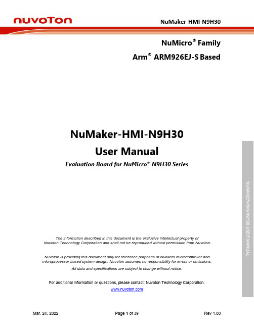
NuMicro®FamilyArm® ARM926EJ-S BasedNuMaker-HMI-N9H30User ManualEvaluation Board for NuMicro® N9H30 SeriesNUMAKER-HMI-N9H30 USER MANUALThe information described in this document is the exclusive intellectual property ofNuvoton Technology Corporation and shall not be reproduced without permission from Nuvoton.Nuvoton is providing this document only for reference purposes of NuMicro microcontroller andmicroprocessor based system design. Nuvoton assumes no responsibility for errors or omissions.All data and specifications are subject to change without notice.For additional information or questions, please contact: Nuvoton Technology Corporation.Table of Contents1OVERVIEW (5)1.1Features (7)1.1.1NuMaker-N9H30 Main Board Features (7)1.1.2NuDesign-TFT-LCD7 Extension Board Features (7)1.2Supporting Resources (8)2NUMAKER-HMI-N9H30 HARDWARE CONFIGURATION (9)2.1NuMaker-N9H30 Board - Front View (9)2.2NuMaker-N9H30 Board - Rear View (14)2.3NuDesign-TFT-LCD7 - Front View (20)2.4NuDesign-TFT-LCD7 - Rear View (21)2.5NuMaker-N9H30 and NuDesign-TFT-LCD7 PCB Placement (22)3NUMAKER-N9H30 AND NUDESIGN-TFT-LCD7 SCHEMATICS (24)3.1NuMaker-N9H30 - GPIO List Circuit (24)3.2NuMaker-N9H30 - System Block Circuit (25)3.3NuMaker-N9H30 - Power Circuit (26)3.4NuMaker-N9H30 - N9H30F61IEC Circuit (27)3.5NuMaker-N9H30 - Setting, ICE, RS-232_0, Key Circuit (28)NUMAKER-HMI-N9H30 USER MANUAL3.6NuMaker-N9H30 - Memory Circuit (29)3.7NuMaker-N9H30 - I2S, I2C_0, RS-485_6 Circuit (30)3.8NuMaker-N9H30 - RS-232_2 Circuit (31)3.9NuMaker-N9H30 - LCD Circuit (32)3.10NuMaker-N9H30 - CMOS Sensor, I2C_1, CAN_0 Circuit (33)3.11NuMaker-N9H30 - RMII_0_PF Circuit (34)3.12NuMaker-N9H30 - RMII_1_PE Circuit (35)3.13NuMaker-N9H30 - USB Circuit (36)3.14NuDesign-TFT-LCD7 - TFT-LCD7 Circuit (37)4REVISION HISTORY (38)List of FiguresFigure 1-1 Front View of NuMaker-HMI-N9H30 Evaluation Board (5)Figure 1-2 Rear View of NuMaker-HMI-N9H30 Evaluation Board (6)Figure 2-1 Front View of NuMaker-N9H30 Board (9)Figure 2-2 Rear View of NuMaker-N9H30 Board (14)Figure 2-3 Front View of NuDesign-TFT-LCD7 Board (20)Figure 2-4 Rear View of NuDesign-TFT-LCD7 Board (21)Figure 2-5 Front View of NuMaker-N9H30 PCB Placement (22)Figure 2-6 Rear View of NuMaker-N9H30 PCB Placement (22)Figure 2-7 Front View of NuDesign-TFT-LCD7 PCB Placement (23)Figure 2-8 Rear View of NuDesign-TFT-LCD7 PCB Placement (23)Figure 3-1 GPIO List Circuit (24)Figure 3-2 System Block Circuit (25)Figure 3-3 Power Circuit (26)Figure 3-4 N9H30F61IEC Circuit (27)Figure 3-5 Setting, ICE, RS-232_0, Key Circuit (28)Figure 3-6 Memory Circuit (29)Figure 3-7 I2S, I2C_0, RS-486_6 Circuit (30)Figure 3-8 RS-232_2 Circuit (31)Figure 3-9 LCD Circuit (32)NUMAKER-HMI-N9H30 USER MANUAL Figure 3-10 CMOS Sensor, I2C_1, CAN_0 Circuit (33)Figure 3-11 RMII_0_PF Circuit (34)Figure 3-12 RMII_1_PE Circuit (35)Figure 3-13 USB Circuit (36)Figure 3-14 TFT-LCD7 Circuit (37)List of TablesTable 2-1 LCD Panel Combination Connector (CON8) Pin Function (11)Table 2-2 Three Sets of Indication LED Functions (12)Table 2-3 Six Sets of User SW, Key Matrix Functions (12)Table 2-4 CMOS Sensor Connector (CON10) Function (13)Table 2-5 JTAG ICE Interface (J2) Function (14)Table 2-6 Expand Port (CON7) Function (16)Table 2-7 UART0 (J3) Function (16)Table 2-8 UART2 (J6) Function (16)Table 2-9 RS-485_6 (SW6~8) Function (17)Table 2-10 Power on Setting (SW4) Function (17)Table 2-11 Power on Setting (S2) Function (17)Table 2-12 Power on Setting (S3) Function (17)Table 2-13 Power on Setting (S4) Function (17)Table 2-14 Power on Setting (S5) Function (17)Table 2-15 Power on Setting (S7/S6) Function (18)Table 2-16 Power on Setting (S9/S8) Function (18)Table 2-17 CMOS Sensor Connector (CON9) Function (19)Table 2-18 CAN_0 (SW9~10) Function (19)NUMAKER-HMI-N9H30 USER MANUAL1 OVERVIEWThe NuMaker-HMI-N9H30 is an evaluation board for GUI application development. The NuMaker-HMI-N9H30 consists of two parts: a NuMaker-N9H30 main board and a NuDesign-TFT-LCD7 extensionboard. The NuMaker-HMI-N9H30 is designed for project evaluation, prototype development andvalidation with HMI (Human Machine Interface) function.The NuMaker-HMI-N9H30 integrates touchscreen display, voice input/output, rich serial port serviceand I/O interface, providing multiple external storage methods.The NuDesign-TFT-LCD7 can be plugged into the main board via the DIN_32x2 extension connector.The NuDesign-TFT-LCD7 includes one 7” LCD which the resolution is 800x480 with RGB-24bits andembedded the 4-wires resistive type touch panel.Figure 1-1 Front View of NuMaker-HMI-N9H30 Evaluation BoardNUMAKER-HMI-N9H30 USER MANUAL Figure 1-2 Rear View of NuMaker-HMI-N9H30 Evaluation Board1.1 Features1.1.1 NuMaker-N9H30 Main Board Features●N9H30F61IEC chip: LQFP216 pin MCP package with DDR (64 MB)●SPI Flash using W25Q256JVEQ (32 MB) booting with quad mode or storage memory●NAND Flash using W29N01HVSINA (128 MB) booting or storage memory●One Micro-SD/TF card slot served either as a SD memory card for data storage or SDIO(Wi-Fi) device●Two sets of COM ports:–One DB9 RS-232 port with UART_0 used 75C3232E transceiver chip can be servedfor function debug and system development.–One DB9 RS-232 port with UART_2 used 75C3232E transceiver chip for userapplication●22 GPIO expansion ports, including seven sets of UART functions●JTAG interface provided for software development●Microphone input and Earphone/Speaker output with 24-bit stereo audio codec(NAU88C22) for I2S interfaces●Six sets of user-configurable push button keys●Three sets of LEDs for status indication●Provides SN65HVD230 transceiver chip for CAN bus communication●Provides MAX3485 transceiver chip for RS-485 device connection●One buzzer device for program applicationNUMAKER-HMI-N9H30 USER MANUAL●Two sets of RJ45 ports with Ethernet 10/100 Mbps MAC used IP101GR PHY chip●USB_0 that can be used as Device/HOST and USB_1 that can be used as HOSTsupports pen drives, keyboards, mouse and printers●Provides over-voltage and over current protection used APL3211A chip●Retain RTC battery socket for CR2032 type and ADC0 detect battery voltage●System power could be supplied by DC-5V adaptor or USB VBUS1.1.2 NuDesign-TFT-LCD7 Extension Board Features●7” resolution 800x480 4-wire resistive touch panel for 24-bits RGB888 interface●DIN_32x2 extension connector1.2 Supporting ResourcesFor sample codes and introduction about NuMaker-N9H30, please refer to N9H30 BSP:https:///products/gui-solution/gui-platform/numaker-hmi-n9h30/?group=Software&tab=2Visit NuForum for further discussion about the NuMaker-HMI-N9H30:/viewforum.php?f=31 NUMAKER-HMI-N9H30 USER MANUALNUMAKER-HMI-N9H30 USER MANUAL2 NUMAKER-HMI-N9H30 HARDWARE CONFIGURATION2.1 NuMaker-N9H30 Board - Front View Combination Connector (CON8)6 set User SWs (K1~6)3set Indication LEDs (LED1~3)Power Supply Switch (SW_POWER1)Audio Codec(U10)Microphone(M1)NAND Flash(U9)RS-232 Transceiver(U6, U12)RS-485 Transceiver(U11)CAN Transceiver (U13)Figure 2-1 Front View of NuMaker-N9H30 BoardFigure 2-1 shows the main components and connectors from the front side of NuMaker-N9H30 board. The following lists components and connectors from the front view:NuMaker-N9H30 board and NuDesign-TFT-LCD7 board combination connector (CON8). This panel connector supports 4-/5-wire resistive touch or capacitance touch panel for 24-bits RGB888 interface.Connector GPIO pin of N9H30 FunctionCON8.1 - Power 3.3VCON8.2 - Power 3.3VCON8.3 GPD7 LCD_CSCON8.4 GPH3 LCD_BLENCON8.5 GPG9 LCD_DENCON8.7 GPG7 LCD_HSYNCCON8.8 GPG6 LCD_CLKCON8.9 GPD15 LCD_D23(R7)CON8.10 GPD14 LCD_D22(R6)CON8.11 GPD13 LCD_D21(R5)CON8.12 GPD12 LCD_D20(R4)CON8.13 GPD11 LCD_D19(R3)CON8.14 GPD10 LCD_D18(R2)CON8.15 GPD9 LCD_D17(R1)CON8.16 GPD8 LCD_D16(R0)CON8.17 GPA15 LCD_D15(G7)CON8.18 GPA14 LCD_D14(G6)CON8.19 GPA13 LCD_D13(G5)CON8.20 GPA12 LCD_D12(G4)CON8.21 GPA11 LCD_D11(G3)CON8.22 GPA10 LCD_D10(G2)CON8.23 GPA9 LCD_D9(G1) NUMAKER-HMI-N9H30 USER MANUALCON8.24 GPA8 LCD_D8(G0)CON8.25 GPA7 LCD_D7(B7)CON8.26 GPA6 LCD_D6(B6)CON8.27 GPA5 LCD_D5(B5)CON8.28 GPA4 LCD_D4(B4)CON8.29 GPA3 LCD_D3(B3)CON8.30 GPA2 LCD_D2(B2)CON8.31 GPA1 LCD_D1(B1)CON8.32 GPA0 LCD_D0(B0)CON8.33 - -CON8.34 - -CON8.35 - -CON8.36 - -CON8.37 GPB2 LCD_PWMCON8.39 - VSSCON8.40 - VSSCON8.41 ADC7 XPCON8.42 ADC3 VsenCON8.43 ADC6 XMCON8.44 ADC4 YMCON8.45 - -CON8.46 ADC5 YPCON8.47 - VSSCON8.48 - VSSCON8.49 GPG0 I2C0_CCON8.50 GPG1 I2C0_DCON8.51 GPG5 TOUCH_INTCON8.52 - -CON8.53 - -CON8.54 - -CON8.55 - -NUMAKER-HMI-N9H30 USER MANUAL CON8.56 - -CON8.57 - -CON8.58 - -CON8.59 - VSSCON8.60 - VSSCON8.61 - -CON8.62 - -CON8.63 - Power 5VCON8.64 - Power 5VTable 2-1 LCD Panel Combination Connector (CON8) Pin Function●Power supply switch (SW_POWER1): System will be powered on if the SW_POWER1button is pressed●Three sets of indication LEDs:LED Color DescriptionsLED1 Red The system power will beterminated and LED1 lightingwhen the input voltage exceeds5.7V or the current exceeds 2A.LED2 Green Power normal state.LED3 Green Controlled by GPH2 pin Table 2-2 Three Sets of Indication LED Functions●Six sets of user SW, Key Matrix for user definitionKey GPIO pin of N9H30 FunctionK1 GPF10 Row0 GPB4 Col0K2 GPF10 Row0 GPB5 Col1K3 GPE15 Row1 GPB4 Col0K4 GPE15 Row1 GPB5 Col1K5 GPE14 Row2 GPB4 Col0K6GPE14 Row2GPB5 Col1 Table 2-3 Six Sets of User SW, Key Matrix Functions●NAND Flash (128 MB) with Winbond W29N01HVS1NA (U9)●Microphone (M1): Through Nuvoton NAU88C22 chip sound input●Audio CODEC chip (U10): Nuvoton NAU88C22 chip connected to N9H30 using I2Sinterface–SW6/SW7/SW8: 1-2 short for RS-485_6 function and connected to 2P terminal (CON5and J5)–SW6/SW7/SW8: 2-3 short for I2S function and connected to NAU88C22 (U10).●CMOS Sensor connector (CON10, SW9~10)–SW9~10: 1-2 short for CAN_0 function and connected to 2P terminal (CON11)–SW9~10: 2-3 short for CMOS sensor function and connected to CMOS sensorconnector (CON10)Connector GPIO pin of N9H30 FunctionCON10.1 - VSSCON10.2 - VSSNUMAKER-HMI-N9H30 USER MANUALCON10.3 - Power 3.3VCON10.4 - Power 3.3VCON10.5 - -CON10.6 - -CON10.7 GPI4 S_PCLKCON10.8 GPI3 S_CLKCON10.9 GPI8 S_D0CON10.10 GPI9 S_D1CON10.11 GPI10 S_D2CON10.12 GPI11 S_D3CON10.13 GPI12 S_D4CON10.14 GPI13 S_D5CON10.15 GPI14 S_D6CON10.16 GPI15 S_D7CON10.17 GPI6 S_VSYNCCON10.18 GPI5 S_HSYNCCON10.19 GPI0 S_PWDNNUMAKER-HMI-N9H30 USER MANUAL CON10.20 GPI7 S_nRSTCON10.21 GPG2 I2C1_CCON10.22 GPG3 I2C1_DCON10.23 - VSSCON10.24 - VSSTable 2-4 CMOS Sensor Connector (CON10) FunctionNUMAKER-HMI-N9H30 USER MANUAL2.2NuMaker-N9H30 Board - Rear View5V In (CON1)RS-232 DB9 (CON2,CON6)Expand Port (CON7)Speaker Output (J4)Earphone Output (CON4)Buzzer (BZ1)System ResetSW (SW5)SPI Flash (U7,U8)JTAG ICE (J2)Power ProtectionIC (U1)N9H30F61IEC (U5)Micro SD Slot (CON3)RJ45 (CON12, CON13)USB1 HOST (CON15)USB0 Device/Host (CON14)CAN_0 Terminal (CON11)CMOS Sensor Connector (CON9)Power On Setting(SW4, S2~S9)RS-485_6 Terminal (CON5)RTC Battery(BT1)RMII PHY (U14,U16)Figure 2-2 Rear View of NuMaker-N9H30 BoardFigure 2-2 shows the main components and connectors from the rear side of NuMaker-N9H30 board. The following lists components and connectors from the rear view:● +5V In (CON1): Power adaptor 5V input ●JTAG ICE interface (J2) ConnectorGPIO pin of N9H30Function J2.1 - Power 3.3V J2.2 GPJ4 nTRST J2.3 GPJ2 TDI J2.4 GPJ1 TMS J2.5 GPJ0 TCK J2.6 - VSS J2.7 GPJ3 TD0 J2.8-RESETTable 2-5 JTAG ICE Interface (J2) Function●SPI Flash (32 MB) with Winbond W25Q256JVEQ (U7); only one (U7 or U8) SPI Flashcan be used●System Reset (SW5): System will be reset if the SW5 button is pressed●Buzzer (BZ1): Control by GPB3 pin of N9H30●Speaker output (J4): Through the NAU88C22 chip sound output●Earphone output (CON4): Through the NAU88C22 chip sound output●Expand port for user use (CON7):Connector GPIO pin of N9H30 FunctionCON7.1 - Power 3.3VCON7.2 - Power 3.3VCON7.3 GPE12 UART3_TXDCON7.4 GPH4 UART1_TXDCON7.5 GPE13 UART3_RXDCON7.6 GPH5 UART1_RXDCON7.7 GPB0 UART5_TXDCON7.8 GPH6 UART1_RTSCON7.9 GPB1 UART5_RXDCON7.10 GPH7 UART1_CTSCON7.11 GPI1 UART7_TXDNUMAKER-HMI-N9H30 USER MANUAL CON7.12 GPH8 UART4_TXDCON7.13 GPI2 UART7_RXDCON7.14 GPH9 UART4_RXDCON7.15 - -CON7.16 GPH10 UART4_RTSCON7.17 - -CON7.18 GPH11 UART4_CTSCON7.19 - VSSCON7.20 - VSSCON7.21 GPB12 UART10_TXDCON7.22 GPH12 UART8_TXDCON7.23 GPB13 UART10_RXDCON7.24 GPH13 UART8_RXDCON7.25 GPB14 UART10_RTSCON7.26 GPH14 UART8_RTSCON7.27 GPB15 UART10_CTSCON7.28 GPH15 UART8_CTSCON7.29 - Power 5VCON7.30 - Power 5VTable 2-6 Expand Port (CON7) Function●UART0 selection (CON2, J3):–RS-232_0 function and connected to DB9 female (CON2) for debug message output.–GPE0/GPE1 connected to 2P terminal (J3).Connector GPIO pin of N9H30 Function J3.1 GPE1 UART0_RXDJ3.2 GPE0 UART0_TXDTable 2-7 UART0 (J3) Function●UART2 selection (CON6, J6):–RS-232_2 function and connected to DB9 female (CON6) for debug message output –GPF11~14 connected to 4P terminal (J6)Connector GPIO pin of N9H30 Function J6.1 GPF11 UART2_TXDJ6.2 GPF12 UART2_RXDJ6.3 GPF13 UART2_RTSJ6.4 GPF14 UART2_CTSTable 2-8 UART2 (J6) Function●RS-485_6 selection (CON5, J5, SW6~8):–SW6~8: 1-2 short for RS-485_6 function and connected to 2P terminal (CON5 and J5) –SW6~8: 2-3 short for I2S function and connected to NAU88C22 (U10)Connector GPIO pin of N9H30 FunctionSW6:1-2 shortGPG11 RS-485_6_DISW6:2-3 short I2S_DOSW7:1-2 shortGPG12 RS-485_6_ROSW7:2-3 short I2S_DISW8:1-2 shortGPG13 RS-485_6_ENBSW8:2-3 short I2S_BCLKNUMAKER-HMI-N9H30 USER MANUALTable 2-9 RS-485_6 (SW6~8) FunctionPower on setting (SW4, S2~9).SW State FunctionSW4.2/SW4.1 ON/ON Boot from USB SW4.2/SW4.1 ON/OFF Boot from eMMC SW4.2/SW4.1 OFF/ON Boot from NAND Flash SW4.2/SW4.1 OFF/OFF Boot from SPI Flash Table 2-10 Power on Setting (SW4) FunctionSW State FunctionS2 Short System clock from 12MHzcrystalS2 Open System clock from UPLL output Table 2-11 Power on Setting (S2) FunctionSW State FunctionS3 Short Watchdog Timer OFFS3 Open Watchdog Timer ON Table 2-12 Power on Setting (S3) FunctionSW State FunctionS4 Short GPJ[4:0] used as GPIO pinS4Open GPJ[4:0] used as JTAG ICEinterfaceTable 2-13 Power on Setting (S4) FunctionSW State FunctionS5 Short UART0 debug message ONS5 Open UART0 debug message OFFTable 2-14 Power on Setting (S5) FunctionSW State FunctionS7/S6 Short/Short NAND Flash page size 2KBS7/S6 Short/Open NAND Flash page size 4KBS7/S6 Open/Short NAND Flash page size 8KBNUMAKER-HMI-N9H30 USER MANUALS7/S6 Open/Open IgnoreTable 2-15 Power on Setting (S7/S6) FunctionSW State FunctionS9/S8 Short/Short NAND Flash ECC type BCH T12S9/S8 Short/Open NAND Flash ECC type BCH T15S9/S8 Open/Short NAND Flash ECC type BCH T24S9/S8 Open/Open IgnoreTable 2-16 Power on Setting (S9/S8) FunctionCMOS Sensor connector (CON9, SW9~10)–SW9~10: 1-2 short for CAN_0 function and connected to 2P terminal (CON11).–SW9~10: 2-3 short for CMOS sensor function and connected to CMOS sensorconnector (CON9).Connector GPIO pin of N9H30 FunctionCON9.1 - VSSCON9.2 - VSSCON9.3 - Power 3.3VCON9.4 - Power 3.3V NUMAKER-HMI-N9H30 USER MANUALCON9.5 - -CON9.6 - -CON9.7 GPI4 S_PCLKCON9.8 GPI3 S_CLKCON9.9 GPI8 S_D0CON9.10 GPI9 S_D1CON9.11 GPI10 S_D2CON9.12 GPI11 S_D3CON9.13 GPI12 S_D4CON9.14 GPI13 S_D5CON9.15 GPI14 S_D6CON9.16 GPI15 S_D7CON9.17 GPI6 S_VSYNCCON9.18 GPI5 S_HSYNCCON9.19 GPI0 S_PWDNCON9.20 GPI7 S_nRSTCON9.21 GPG2 I2C1_CCON9.22 GPG3 I2C1_DCON9.23 - VSSCON9.24 - VSSTable 2-17 CMOS Sensor Connector (CON9) Function●CAN_0 Selection (CON11, SW9~10):–SW9~10: 1-2 short for CAN_0 function and connected to 2P terminal (CON11) –SW9~10: 2-3 short for CMOS sensor function and connected to CMOS sensor connector (CON9, CON10)SW GPIO pin of N9H30 FunctionSW9:1-2 shortGPI3 CAN_0_RXDSW9:2-3 short S_CLKSW10:1-2 shortGPI4 CAN_0_TXDSW10:2-3 short S_PCLKTable 2-18 CAN_0 (SW9~10) Function●USB0 Device/HOST Micro-AB connector (CON14), where CON14 pin4 ID=1 is Device,ID=0 is HOST●USB1 for USB HOST with Type-A connector (CON15)●RJ45_0 connector with LED indicator (CON12), RMII PHY with IP101GR (U14)●RJ45_1 connector with LED indicator (CON13), RMII PHY with IP101GR (U16)●Micro-SD/TF card slot (CON3)●SOC CPU: Nuvoton N9H30F61IEC (U5)●Battery power for RTC 3.3V powered (BT1, J1), can detect voltage by ADC0●RTC power has 3 sources:–Share with 3.3V I/O power–Battery socket for CR2032 (BT1)–External connector (J1)●Board version 2.1NUMAKER-HMI-N9H30 USER MANUAL2.3 NuDesign-TFT-LCD7 -Front ViewFigure 2-3 Front View of NuDesign-TFT-LCD7 BoardFigure 2-3 shows the main components and connectors from the Front side of NuDesign-TFT-LCD7board.7” resolution 800x480 4-W resistive touch panel for 24-bits RGB888 interface2.4 NuDesign-TFT-LCD7 -Rear ViewFigure 2-4 Rear View of NuDesign-TFT-LCD7 BoardFigure 2-4 shows the main components and connectors from the rear side of NuDesign-TFT-LCD7board.NuMaker-N9H30 and NuDesign-TFT-LCD7 combination connector (CON1).NUMAKER-HMI-N9H30 USER MANUAL 2.5 NuMaker-N9H30 and NuDesign-TFT-LCD7 PCB PlacementFigure 2-5 Front View of NuMaker-N9H30 PCB PlacementFigure 2-6 Rear View of NuMaker-N9H30 PCB PlacementNUMAKER-HMI-N9H30 USER MANUALFigure 2-7 Front View of NuDesign-TFT-LCD7 PCB PlacementFigure 2-8 Rear View of NuDesign-TFT-LCD7 PCB Placement3 NUMAKER-N9H30 AND NUDESIGN-TFT-LCD7 SCHEMATICS3.1 NuMaker-N9H30 - GPIO List CircuitFigure 3-1 shows the N9H30F61IEC GPIO list circuit.Figure 3-1 GPIO List Circuit NUMAKER-HMI-N9H30 USER MANUAL3.2 NuMaker-N9H30 - System Block CircuitFigure 3-2 shows the System Block Circuit.NUMAKER-HMI-N9H30 USER MANUALFigure 3-2 System Block Circuit3.3 NuMaker-N9H30 - Power CircuitFigure 3-3 shows the Power Circuit.NUMAKER-HMI-N9H30 USER MANUALFigure 3-3 Power Circuit3.4 NuMaker-N9H30 - N9H30F61IEC CircuitFigure 3-4 shows the N9H30F61IEC Circuit.Figure 3-4 N9H30F61IEC CircuitNUMAKER-HMI-N9H30 USER MANUAL3.5 NuMaker-N9H30 - Setting, ICE, RS-232_0, Key CircuitFigure 3-5 shows the Setting, ICE, RS-232_0, Key Circuit.NUMAKER-HMI-N9H30 USER MANUALFigure 3-5 Setting, ICE, RS-232_0, Key Circuit3.6 NuMaker-N9H30 - Memory CircuitFigure 3-6 shows the Memory Circuit.NUMAKER-HMI-N9H30 USER MANUALFigure 3-6 Memory Circuit3.7 NuMaker-N9H30 - I2S, I2C_0, RS-485_6 CircuitFigure 3-7 shows the I2S, I2C_0, RS-486_6 Circuit.NUMAKER-HMI-N9H30 USER MANUALFigure 3-7 I2S, I2C_0, RS-486_6 Circuit3.8 NuMaker-N9H30 - RS-232_2 CircuitFigure 3-8 shows the RS-232_2 Circuit.NUMAKER-HMI-N9H30 USER MANUALFigure 3-8 RS-232_2 Circuit3.9 NuMaker-N9H30 - LCD CircuitFigure 3-9 shows the LCD Circuit.NUMAKER-HMI-N9H30 USER MANUALFigure 3-9 LCD Circuit3.10 NuMaker-N9H30 - CMOS Sensor, I2C_1, CAN_0 CircuitFigure 3-10 shows the CMOS Sensor,I2C_1, CAN_0 Circuit.NUMAKER-HMI-N9H30 USER MANUALFigure 3-10 CMOS Sensor, I2C_1, CAN_0 Circuit3.11 NuMaker-N9H30 - RMII_0_PF CircuitFigure 3-11 shows the RMII_0_RF Circuit.NUMAKER-HMI-N9H30 USER MANUALFigure 3-11 RMII_0_PF Circuit3.12 NuMaker-N9H30 - RMII_1_PE CircuitFigure 3-12 shows the RMII_1_PE Circuit.NUMAKER-HMI-N9H30 USER MANUALFigure 3-12 RMII_1_PE Circuit3.13 NuMaker-N9H30 - USB CircuitFigure 3-13 shows the USB Circuit.NUMAKER-HMI-N9H30 USER MANUALFigure 3-13 USB Circuit3.14 NuDesign-TFT-LCD7 - TFT-LCD7 CircuitFigure 3-14 shows the TFT-LCD7 Circuit.Figure 3-14 TFT-LCD7 CircuitNUMAKER-HMI-N9H30 USER MANUAL4 REVISION HISTORYDate Revision Description2022.03.24 1.00 Initial version NUMAKER-HMI-N9H30 USER MANUALNUMAKER-HMI-N9H30 USER MANUALImportant NoticeNuvoton Products are neither intended nor warranted for usage in systems or equipment, anymalfunction or failure of which may cause loss of human life, bodily injury or severe propertydamage. Such applications are deemed, “Insecure Usage”.Insecure usage includes, but is not limited to: equipment for surgical implementation, atomicenergy control instruments, airplane or spaceship instruments, the control or operation ofdynamic, brake or safety systems designed for vehicular use, traffic signal instruments, all typesof safety devices, and other applications intended to support or sustain life.All Insecure Usage shall be made at customer’s risk, and in the event that third parties lay claimsto Nuvoton as a result of customer’s Insecure Usage, custome r shall indemnify the damagesand liabilities thus incurred by Nuvoton.。
KSZ8851-16MLL DEMO BOARD 48-PIN ETHERNET CONTROLLE

SD13
SD7 40
CPU_D14 3
6
SD14
SD8 39
CPU_D15 4
5
SD15
SD9 36
SD10 35
33
SD11 34
CPU_CMD
33
SD12 33
R10
SD13 32
CPU_CSN
33
SD14 31
R12
SD15 30
CPU_WRN
33
CMD
11
R14
CPU_RDN
33
CSN
12
R16
5 6 7 8
TANT
C27
R28 10uF
470pF 2.49K
Power 3.3V 0.1uF (red LED)
CSN CMD
4.7K R27 4.7K R29
GBLC03C_0 D3
GND 2 GND
VR 5 3.3VA
INTRN 4.7K R30
VOUT = 1.24 X [ 1 + ( 2.49k/ 1.5K ) ]
5
4
3
KSZ8851-16MLL (48-pin) Demo Board Black Diagram
D
Headers 20x2
RJ45
LAN1 T
KSZ8851-16MLL
Reset
Power
+1.8V
+2.5V
+3.3V
STATUS LEDs
OSC
EEPROM
C
MIC5209YM
25 MHz
AT93C46
x2
2
1
DATE:
MC9RS08KA8微控制器单元说明书

Target Applications • High-brightness LED • Lighting systems control • Toys• Small handheld devices• Space-constrained applications • Small appliances• AC line voltage monitoring • Battery charger • ASIC replacement OverviewThe MC9RS08KA8 microcontroller unit (MCU) is an extremely cost-effective and highly integrated, device intended for home appliances, health care equipment and as a general-purpose microcontroller. This device is composed of standard on-chip modules including a very small and highly efficient RS08 CPU core, 254 bytes RAM, 8K bytes flash, two 8-bit modulo timers,12-channel 10-bit ADC, 2-channel 16-bit timer/PWM, inter-integrated circuit bus module, keyboard interrupt and analog comparator. The device is available in 16- and 20-pin packages.Cost-Effective Development toolsFor more information on development tools, please refer to the Freescale Development Tool Selector Guide (SG1011).CodeWarrior ® Development Studio for Microcontrollers 6.1Complimentary*CodeWarrior Development Studio for Microcontrollers is an integrated tool suite that supports software development for Freescale’s 8-bit or 32-bit microcontrollers. Designers can further accelerate application development with the help of the Processor Expert™ tool, which is an award-winning rapid application development tool in the CodeWarrior tool suite.DEMO9RS08KA8$50 MSRPCost-effective demonstration board with potentiometer, LEDs and a built-in USB-BDM cable for debugging and programming.8-bit MicrocontrollersMC9RS08KA8/4Package OptionsPart NumberPackageTemp. Range* Subject to license agreement and registrationFreescale and the Freescale logo are trademarks or registered trademarks of Freescale Semiconductor, Inc. in the U.S. and other countries. All other product or service names are the property of their respective owners. © Freescale Semiconductor, Inc. 2008.Document Number: MC9RS08KA8/4FSREV 1。
NSG 435 ESD Simulator User Manual

1NSG 435 ESD SIMULATORUSER MANUAL5.4 Air/Contact-discharge 28 5.5 Voltage 29 5.6 Polarity 30 5.7 Repetition frequency 31 5.8 Counter 31 5.9 Preselect counter 32 5.10 Automatic polarity switching 34 5.11 Continuous operation 375.12 Storing voltage settings 396 Test procedures 41 6.1 Standard-conforms procedures 416.2 Other conditions 417 Verification of the pulse data 438 Maintenance 44 8.1 Servicing 44 8.2 Calibration 44 8.3 Exchanging the R/C network 47 8.3.1 Derating of pulse repetition at increased capacitance 49 8.4 Repairs 508.5 Disposal 509 Declaration of Conformity CE 5110 Technical specifications 5211 ESD standards 5412 Warranty 5513 Odering information 5614 Addresses 57discharge network (exchangeable)measuring electronicshigh voltage relaypolarity changeovertrigger connection Test finger (exchangeable)Earth cableconnectionPulse triggerExchangeablebattery packTripod bushUNC1/4-20HandgripF1 Toggle between air and contact-discharge (and vice versa) Increment voltage and counterF2 Activation of voltage settingDecrement voltage and counterF3 Polarity switching:Selection of pre-programmed test levelsPreselect counter on/offF4 Selection of discharge mode:Single discharge Repetitive discharge at 0.5, 1, 5, 10, 20, 25 Hzfor air-dischargeRepetitive discharge at 0.5, 1, 5, 10 Hz for contact-dischargeAutomatic polarity switchingStorage of programmed test levelsF5 Resets the counterReturn from second functionNSG 435 ESD simulatorposes.The handgrip adapter is an integral part of this power supply unit. It contains electrical components that are necessary for this mode of operation. It is not per-missible to operate the NSG 435 with a power supply unit from another system.The power supply unit can be used on all common AC mains supplies without having to make any adjustments, thus:80 to 240 V (50/60 Hz) with 3-pin IEC connectorMatching 3-core mains cable20NSG 435 ESD simulator The power supply unit must be connected to a mains outlet having a protectiveearth.The protective earth connection does not replace the earth cable for the opera-tion of the NSG 435. To ensure safe and valid test operation the earth cable must be correctly connected as the pulse return path in every case.The mains power supply unit is constructed in conformity with the relevant safety standards and carries the appropriate test symbol.3.3.5 Discharge networksThe basic set contains a discharge network and test fingers that conforms to IEC/EN 61000-4-2, Ed. 1.2:2001.Alternative networks can be installed for testing in accordance with other standards.The discharge network and test fingers form a mutually matched combination. They are labeled with a corresponding INA number. The specified pulse data are only achieved while this combination is maintained.Several combinations are given in the order list. The C and R values of the discharge network can also be specified for other applications.Networks conforming to other standards can be built upon request. The speci-fications of the standard must be fully defined.Exchanging the discharge network is described in section «Exchanging the R/C network».The normal remote trigger unit consists of a «triggerbox» and 5 m (197 “) of optical cable. The remote trigger works in parallel with the «trigger-button» on the NSG 435. Pulse triggering, or the on/off switching in the case of repetitive discharges, can be effected by a push-button or an electrical signal applied to the triggerbox.The electrical signal at the BNC connector must fulfill the following condi tions:On: V = 2.4...10 V, I >2 mA, t >10 msOff: V <0.8 VRepetition rate: <5 HzThe remote trigger is powered by a conventional 9 volt battery. The current consumption is so low that a battery switch has been dispensed with. If NSG 435 provided with two optical connectors connect the optical cable to the blue terminal.It is recommended to remove the battery if the unit is not going to be used forMounting flangeContact surfaceThe measurement adapter type MD 101 as per informative annex B of IEC/EN 61000-4-2 serves to verify pulse amplitudes and pulse shapes. It is designed for mounting in the side wall of a Faraday cage in which an oscilloscope has been installed. This measurement adapter, also known as a «Pellegrini-Target» has the flat impedance curve to well over 1 GHz that is necessary for the purpose. Use of this adapter is only worthwhile in conjunction with a test rig that is laid out in strict conformity with the relevant standard (see section 7).24NSG 435 ESD simulatorSwitch the simulator on with the main switch.A display appears in the window showing values representing the status of the instrument before it was last switched off.A typical set of values might look like this:The instrument performs audible switching functions for a while that result from various self-tests and calibration procedures.High voltage generation is activated by pressing and holding the trigger button. By bringing the test finger close to the earthing point an discharge occurs which is acknowledged acoustically and the display shows the effective discharge voltage in a frame. (This applies under the following conditions: air-discharge, single-pulse, preselect counter off).The instrument is now ready to use.26NSG 435 ESD simulatorThe instrument is ready for use immediately after the execution of a self-testand calibration procedure.Press and hold the trigger button to activate the high voltage generation. The active high voltage state is shown on the display by the “kV” indication blink-ing.The measured value of the breakdown voltage in air-discharge mode will be displayed. Differentiation from the display of the set value is made by the frame around the kV readings.The effective discharge voltage depends on various factors such as the distance to the discharge point, speed of approach, nature of the EUT, etc.In the case of a contact-discharge this measurement is not carried out since only a discharge current can occur.The instrument switches itself off automatically after a period of 30 minutes of non-use although the parameters that have been set will remain stored in memory.The change to contact-discharge is prevented if:The voltage set for this operating mode is too high, i.e. over 9 kVThe repetition frequency set for this operating mode is too high, i.e.over 10 pulses/sThe instrument notifies the error with a beep and the erroneous setting blinks for 5 s.When working with fixed voltage levels, the relevant value is automatically loaded upon toggling between the air/contact-discharge mode.12Free setting Call stored values level 1-4(4 values each for air-dischargeand contact discharge) Pressing F1 or F2 raises or lowers Press F3 to select the four stored the voltage respectively in steps of voltage values in each case. 100 V. Pressing the buttons (To change a stored value, see continuously changes the voltage section 5.12).level with increasing rapidity.30NSG 435 ESD simulatorPress F5 to return to the starting menu level. (This return will also be madeautomatically after about 10 s).5.6 PolarityF3 toggles between positive and negative polarity. The sign shown in the displayalters correspondingly.In the SINGLE mode a discharge is released each time the trigger button is pressed. The discharge is confirmed by a beep. In the REPETITIVE mode dis charges are released at the chosen rate for as long as the trigger button remains pressed (no acoustic confirmation).32NSG 435 ESD simulatorF5 sets the counter either back to 0000 or to the preset value if the preselect counter mode has been chosen.Pressing F5 a second time causes a branch to the preselect counter menu.5.9 Preselect counterA specified number of discharges (0...9999) can be pre-programmed with this function. These can then be triggered single by hand or automatically.F5 first resets the counter then, when pressed a second time, branches into the preselect counter menu.F3 switches the preselect counter operation on and off (PRESELECT ON/OFF). Use F1 and F2 to raise or lower the preset value. Keeping either button pressed causes the change to occur with increasing rapidity.34NSG 435 ESD simulatorPress F5 to return to the original menu level. (This return also occurs automati-cally after about 10 s)The preselect counter mode can be used with either single or with repetitive discharges.Each time there is a discharge the counter content is decremented by 1.In the repetitive mode the discharge sequence is started when the trigger button is first pressed and is halted when the button is pressed a second time. The sequence can be continued by pressing it again.Pulse triggering is terminated when the counter content reaches 0000.F5 reloads the preselect counter with the original value.Once the counter reaches 0000 and the procedure has been stopped, the counter can also be reloaded with the original value again and the test sequence started anew simply by pressing the trigger button.5.10 Automatic polarity switchingThe IEC standards call for equal quantities of positive and then negative dis-charges to be applied to a test point. The NSG 435 can execute this function automatically.The automatic polarity switch operates in conjunction with the preselect counter.F5 branches into the preselect counter menu.F4 switches the function «Automatic polarity change» on and off (Precondition: PRESELECT ON). The active state is shown by the polarity sign in front of the voltage alternating on the display.36NSG 435 ESD simulatorUse F5 to return to the original menu level. (This return also occurs automatically after about 10 s). The «Automatic polarity change» function is identified by «ALT.POL.» over F4 and +/- over F3.The instrument switches over from positive to negative polarity once half of the preset number of pulses has been released (the sign on the display changes).This automatic function works in both the single pulse mode as well as with repetitive discharges.Reinitialize the operation in single pulse mode after each cycle. Reset the counter and select the counter menu again (press F5 three times).Select the repetition frequency in the basic menu with F4. By F5 branch into the preselect counter menu.38NSG 435 ESD simulatorHold F2 down until the counter content is 0000. Press F2 again to activate continuous operation. The display shows - - - -.Use F5 to return to the original menu level.Switching off continuous operation:By F5 branch into the preselect counter menu. Press F1 or F2. The counter shows 0000 or 9999 respectively. Continuous operation is switched off.Use F5 to return to the original menu level.5.12 Storing voltage settingsPre-programmed discharge voltage values can be stored in four memory loca-tions for both air and contact-discharges. As delivered, the instrument has the test levels set according to IEC/EN 61000-4-2, Ed. 1.2:2001.The values stored in memory can be altered arbitrarily.Level Test voltage contact-discharge 1234 2 kV 4 kV 6 kV 8 kV40NSG 435 ESD simulator Press F4 and a memory location (1 ... 4) appears over F3.Use F3 to specify the required memory location. Press F4 again and the value is stored.Use F5 to return to the original menu level.Set the required voltage with F1 or F2.Range for air: 0.2 ... 16.5 kVRange for contact: 0.2 ...9 kVThe «LEVEL» indication shown over F3 disappears. «STORE» appears over F4.simulator46 537A yellowB black8C yellow/green48NSG 435 ESD simulator Procedure:1 Switch the instrument off2 Remove the earth cable3 Take out the battery4 Unscrew the test finger5 Pull out the trigger button6 Remove the rear cover(the cover locks into 3 notches in the housing on both sides. The cover can be removed by carefully lifting it at the points where the notches are and gradually sliding it back).7 Lay the instrument on its side and remove the screws8 Remove the screw in the printed circuit board9 Remove the upper part of the housing with a rocking movement 10 Note the arrangement of the wiring11 Release the network connecting screws in the given order12 Remove the network13 Insert the replacement network14 Firmly screw the color-coded network connections into place as shown in the illustration15 Take care with the placement of the wires so that none becoming trapped while re-assembling the generator16 Carefully screw the upper part of the housing back into place17 Continue re-assembly in the reverse order of points 8 .. 1 above (attach the test finger belonging to the set!)18 Check the operation of the generator by observing the spark-gap (the high voltage generator adjusts itself automatically to the newnetwork)19 If in doubt, a voltage check can be carried out as given in section 8.220 A calibration measurement is not normally necessary50NSG 435 ESD simulator 8.4 RepairsRepair work is to be executed exclusively by authorized Teseq repair depart-ments. Only original replacement parts and accessories are to be used.Do not continue to use the instrument in the event of mechanical damage occurring. The molded housing also performs insulating and protective func-tions which are only assured as long as it is in its original condition. A damaged instrument should be returned without delay to a Teseq service centre.8.5 DisposalThe following list shows the principal materials that are used in the construction of the NSG 435. The relevant national regulations are to be observed when disposing of the instrument.Item Material RemarkHousing Control unit LCD-display LCD-window Chassis plate HV unit/network HV relay Test finger Battery Charger Carrying case ABS with glass-fiberEpoxy circuit board with SMD componentsGlassAcrylicGalvanized steelPolyurethane block with electr.components and copper wireVarious metals, ceramicvarious insulating MagerialsBrass, plastics, electrical componentsNickel-metal hybrid (>2002) ABS hosuing Epoxy circuit board ABS housing with transformer, PCB with electr, componentsPolyethyleneObserve any specialregulations regardingdisposal of Ni-MHs。
FANUC 0系列参数说明
0 0 0 0
0
0
0
0
0
0
0
0
0
0
0
0
0
0
0
0
0
0
0
0
0
0
0
0
0
0
0
0
0
0
0
0
0Hale Waihona Puke 0000
0
0
0
0
0
0
0
0
0
0
0
0
0
0
0
0
0
0
0
0
0
0
0
表 9 编程参数
10/4 15/7 28/4 29/5 389/2 394/6
PRG9 CPRD EXTS MABS PRG8 WKZRST
O9000—O9999 号程序保护 小数点的含义 外部程序号检索 MDI—B 中,指令取决于 G90/G91 设定 O8000—O8999 号程序保护 自动设工件坐标系时设为 G54
PPD 1:坐标系设定时,相对坐标值亦被预置。 0:坐标系设定时,相对坐标值不被预置。
STP2 1:阅读/穿孔接口的停止位由此 2 位设定。 0:阅读/穿孔接口的停止位由此 1 位设定。 (设定参数 I/O “0”时有效) 注:波特率由参数 NO.0522 设定。
0004 0006 0005 0007
0:坐标值显示的是加上偏置值的实际位置。
SCW 1:最小指令值为英制(机床为英制) 0:最小指令值为米制(机床为米制)
0002
7
6
5
4
3
2
1
0
NFED TFHD HSLE
电脑主板纠错灯指示信息及含义

现在(xiànzài)很多人买的主板都带有DEBUG侦错灯,借此把搜集回来的DEBUG侦错灯指示信息及其含义;拿来共享下........CF 测试(cèshì) CMOS R/W 功能性。
C0 早期的主板设定初始值: - 禁用(jìn yònɡ) shadow RAM - 禁用 L2cache(SURPER 7 构架及后期兼容构架) - 检测基本 chipset 寄存器。
C1 检测内存: -Auto- 检测DRAM(动态随机存取储存器)大小,类型(lèixíng) 和 ECC。
-Auto- 检测L2 cache (SURPER 7 构架及后期兼容构架)C3 映射(yìngshè)BIOS编码到DRAM。
C5 允许chipset将BIOS复制到地址为E000 F000的shadow RAM。
01 将Xgroup编码定位在内存地址中的1000到003 初始化Superio(超级输入输出)_Early(响应)_Init(启动)开关。
053.将空白输出到荧屏。
4.清除CMOS错误。
071.清除 8042 接口。
2.初始化 8042接口自检。
081.检测特殊的键盘控制器型号为Winbond 977 系列超级I/O(输入/输出)芯片。
2.允许使用键盘接口。
0A1.禁用PS/2 老鼠接口.(可选)2.在端口和交换接口检测完成后自动检测键盘和鼠标端口。
(可选)3.重置键盘在发现型号为Winbond 977 系列超级I/O输入/输出芯片后。
0E 检测内存地址为F000h段图像以证明是否它支持 R/ W.如果检测失败,机箱扬声器将发出警报。
10 自动检测FlashROM类型以读取合适的FlashROM R/W 编码。
在ESCD和DMI支持的情况下进入运行时间和区域的地址位F000。
12 使用步骤1’s 运算方式以确定CMOS电路的接口。
MC9RS08KA4_8中文数据手册
3FFE
3FFF
BC(JMP 机器码)
跳转地址高字节
跳转地址低字节
飞 3.4 激活背景调试模式 背景调试功能是由 RS08 核内的 BDC 管理的。在软件开发过程中,BDC 提供了
H 一种分析 MCU 操作方法。 C 有 4 种激活背景调试的方法:
*在 POR 期间或发出背景调试强制复位命令之后,拉 BKGD/MS 引脚为低
3
北京飞锐泰克科技有限公司 tel:010-59831537 fax:010-59831536
手机解锁密码大全

手机解锁密码大全三、GSM手机密笈&e r.b]'a D:V(一)摩托罗拉摩托罗拉所有机锁:按MENU+5+1/2 2f} o U%AT190解锁密码: 20010903T191解锁密码:199807223X8/2X88/998/8088/L2000/7689/T189/C289等初始密码为1234 ;话机密码为000000 ;解锁方法:如无测试卡,则先输入1234,如密码已更改,先按Menu键会出现“修改开锁密码”,按OK键,然后输入000000就会显示四位数的话机密码,如保密码已更改,则只能用测试卡或软件工具解。
2C&r/_F3@X!JT2688/2988万能解锁码:19980722C300解话机锁:20020801摩托罗拉手机出现“话机坏,请送修”:可利用测试卡,输入0205#、0205068#即可修复,无须重写码片。
T2688/2988/988d设置中文:*#0000# ok(插卡)V60/V66/V70解锁:插入测试卡,开机后输入menu+048263*进入测试状态后按18*1总清除,输入18*0是主复位。
V998外文改中文:MENU—左方向键按3下—OK—左方向键按5下—OK—Simplified—CHINESE摩托罗拉2688时间不走修复密诀:将电源1脚和8脚用漆包线短接,必杀!(二)诺基亚初始保密码:12345 W"w2K z k#i)A n5110锁码机解码:在保密码锁死,输入正确保密码无效的情况下,可1、按C键不放,2、按*键不放,3、按*键不放,4、输入04*PIN*PIN*PIN# 解除锁码。
;z8N M4s y!q3210解 SP 锁: 1、按C键 2、按向下键 3、按C键直到屏幕清除 4、按住*键直到其闪烁 5、再按住*键直到其闪烁,输入04*PIN码*PIN 码*PIN 6~,O Y)^/W"K vTN7650恢复出厂设置:*#7370#诺基亚手机省30%电密码:*#746025625# |(H3K诺基亚手机查出厂日期:*#0000#诺基亚能打过进不能呼出:如果显示屏左上角有“2”字,按住#键两秒,再按确认即可;如果没有显示“2”,则按“功能键”+6+1+4+2再按确认即可。
- 1、下载文档前请自行甄别文档内容的完整性,平台不提供额外的编辑、内容补充、找答案等附加服务。
- 2、"仅部分预览"的文档,不可在线预览部分如存在完整性等问题,可反馈申请退款(可完整预览的文档不适用该条件!)。
- 3、如文档侵犯您的权益,请联系客服反馈,我们会尽快为您处理(人工客服工作时间:9:00-18:30)。
Email:
Support: support@
DEMO9RS08KB12 QUICK START GUIDE
Introduction and Default Settings
Install CodeWarrior for Microcontrollers:
Insert the CodeWarrior Development Studio for Microcontrollers CD into a CD / DVD drive. The installation pro-gram will start automatically. If the installation fails to start, start the installation program manually. Open Win-dows Explorer and navigate to the CD / DVD drive where the CodeWarrior disk is inserted. Double click on Launch.exe to launch the installer. Follow the on-screen instructions to install the CodeWarrior IDE and inte-grated programmer.
To Launch the Demo Program:
The DEMO9RS08KB12 ships with a demonstration program preloaded into on-chip FLASH memory. The dem-onstration program converts an analog reading from the POT and the Light Sensor to control the LEDs. The in-ternal TPM is used to flash and LED. ASCII text is echoed to the terminal.
1. Verify the option jumpers are set in default positions. Refer to Figure 1 above.
2. Connect the included A/B USB cable between an open USB port on the host PC and the USB connector on
the target board. Follow the on-screen instructions to install the necessary USB drivers.
3. Rotate the POT fully in both directions. LED1 and LED2 combine to display the POT position.
4. Press SW1. Cover and uncover the light sensor at RZ1. LED1 and LED2 combine to display ambient light
incident on the sensor.
5. Connect a serial cable to the DB9 at J4. Open a terminal program such as AxIDE, and configure for 19200,
8, N, 1. Text typed in the terminal window will echo to the screen
The Quick Start CodeWarrior Project may be downloaded from the Axiom Manufacturing web site at
/support.
Troubleshooting
If the demonstration application fails to function as indicated above, please follow the steps below before contact-ing Freescale Semiconductors. Please refer to the TIC card included in the DEMO9RS08KB12 kit for contact in-formation.
∙Ensure the option jumpers are set to default positions. Refer to Figure 1 above.
∙Ensure the correct version of CodeWarrior is installed and that the KB12 Service Pack is installed
∙Ensure D300 and VDD LED’s are both ON
If the above Troubleshooting Tips fail to correct the problem, please contact Freescale Semiconductors for further assistance. Refer to the Technical Information Card (TIC) included in the kit for contact information. The user may also contact Axiom Manufacturing directly at support@.
2。