DDR2
DDR2原理范文
DDR2原理范文DDR2(Double Data Rate 2 SDRAM)是一种计算机内存模块技术,是DDR SDRAM的后续版本。
与DDR1相比,DDR2具有更高的频率和更低的功耗。
下面将详细介绍DDR2的原理。
1.基本原理DDR2采用异步差动信号传输技术,并且在一个时钟周期内可以传输两倍的数据量,即实现了“双倍数据速率”。
DDR2的主频是内存模块频率的二倍,例如DDR2-800模块的主频为400MHz。
2.内部结构DDR2内部由一系列的存储单元组成,每个存储单元由一个电容和一个开关组成。
存储单元根据行和列的地址选通相应的位线,将数据写入或读取出。
DDR2内部还包括一个控制器单元,用于控制存储单元的读写操作。
3.数据传输DDR2采用“双抖”(double pumping)的方式进行数据传输。
在一个时钟周期内,DDR2可以在上升沿和下降沿两个时刻实现数据的传输,因此达到了双倍数据速率的效果。
4.存储单元DDR2的存储单元由一对互补的位线和电容组成。
当输入信号变化时,电容储存位线上的电荷,在读取操作时,电荷被放大器放大,然后转换为数字信号。
5.控制器单元DDR2的控制器单元负责生成时钟信号、读/写信号和其他控制信号,并控制存储单元的读写操作。
控制器单元还会进行预充电等操作,以提高数据传输速度。
6.省电模式DDR2具有节能模式,当内存空闲时,可以进入自动预充电模式。
在这种模式下,DDR2会将所有的位线预充电至VDD/2,以降低功耗。
7.奇偶校验DDR2还支持奇偶校验功能,可通过校验位对数据进行错误检测和纠正。
这有助于提高存储系统的可靠性和稳定性。
8.地址线结构DDR2的地址线结构包括行地址和列地址,每个地址线能够编码的地址范围由总的内存容量和模块的位宽决定。
地址线的结构对DDR2的性能和容量具有重要影响。
总结:DDR2作为DDRSDRAM的升级版本,通过双倍数据速率、异步差动信号传输技术和省电模式等特性,实现了更高的频率和更低的功耗。
DDR2简介
DDR2简介从1998年的PC100到今天的DDR3,内存技术同CPU前端总线一道经历着速度的提升及带宽的扩展。
虽然DDR3在当今已经量产与使用,DDR2在实际上还担任着内存业界应用最广泛最成熟的中流砥柱的角色。
DDR2 在DDR的基础上将芯片接口时钟频率提高一倍并将工作电压从2.5V降低至1.8V,从而使其能在相对更低的功耗下获得更高的传输速率。
一般情况下,DDR2的输入时钟频率覆盖200/266/333/400/533MHz,传输比特率覆盖400/533/667/800/1066Mb/s /pin。
相对于DDR,由于速度的提升,DDR2在主板设计要求上也有所变化。
内存控制器每Channel可级联的DIMM数从DDR时期的4到8条减少至2到3条,数据线(DQ)上的终端电阻从主板上的分立电阻搬移到了DRAM芯片内部(ODT),数据同步信号(DQS)由单端信号变为单端或差分可选信号。
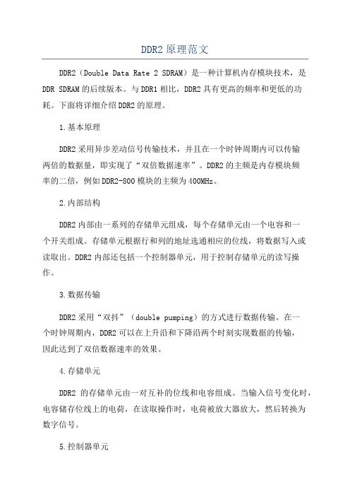
DDR2主板系统架构如右图所示。
图1 DDR2主板系统架构DDR2总线与工作流程以通用计算机主板上的DDR2总线为例,DDR2信号线可以分为数据、命令、时钟3部分。
其中数据线部分主要完成数据传输工作,包括数据线DQ0-63、 Data Mask线DM0-7、数据同步线DQS/DQS# (数据同步线可选单端或差分,通过设定内存芯片内部寄存器EMR[1]的A10位进行选择);命令线部分包括地址线A0-14、Bank选择线 BS0-2、行地址选择RAS#、列选择CAS#、写使能WE#、片选CS#、时钟使能CKE及芯片内部终端电阻使能ODT组成,主要完成寻址、组成各种控制命令及内存初始化工作;差分时钟信号线CK/CK#为整个内存芯片工作提供时钟。
所有的信号线中,除了数据线DQ与数据同步线DQS/DQS#为双向信号线外,其余所有信号线均为单向信号线,只能由内存控制器发出信号。
对于电源和地线,内存颗粒上有一个参考电压输入和三组1.8V电源与地线,分别为芯片上的数据端口,锁相环和芯片电路供电。
ddr2芯片

ddr2芯片DDR2芯片是一种动态随机访问存储器(DRAM)的类型,它是DDR(双倍数据速率)技术的升级版本之一。
DDR2芯片在计算机的内存子系统中起着至关重要的作用。
接下来,我将为您解释关于DDR2芯片的一些重要特点和功能。
首先,DDR2芯片具有更高的传输速率和更大的带宽。
与DDR芯片相比,DDR2芯片的传输速率可以提高到两倍,这意味着数据可以更快地传输到CPU和其他设备。
同时,DDR2芯片的带宽也更大,这意味着它可以在一定时间内处理更多的数据。
其次,DDR2芯片相比DDR芯片有更低的功耗。
DDR2芯片采用了低电压技术,可以在较低的电压下工作,从而减少了能源消耗。
这使得DDR2芯片在节能和延长电池寿命方面具有显著优势,特别是对于笔记本电脑和移动设备来说尤为重要。
此外,DDR2芯片还具有更高的稳定性和可靠性。
DDR2芯片有更强大的误差检测和纠正机制,可以自动检测和修复内存中的错误。
这使得DDR2芯片在数据存储和处理方面更加可靠,提高了整个系统的稳定性。
此外,DDR2芯片还具有更大的容量。
通过DDR2技术的提升,芯片的存储容量也得到了增加。
DDR2芯片可以提供更多的内存空间,允许用户存储更多的数据和程序。
这对于需要处理大型文件和运行多个应用程序的用户来说非常重要。
最后,DDR2芯片具有较长的生命周期。
与其他技术相比,DDR2芯片有较长的可用时间,因为它在市场上被广泛使用,并且许多计算机和移动设备仍然支持DDR2芯片。
这使得DDR2芯片成为一种可靠和稳定的选择,特别是对于需要维护和更新老旧设备的用户来说。
综上所述,DDR2芯片作为一种内存技术,具有更高的传输速率、更大的带宽、更低的功耗、更高的稳定性和可靠性、更大的容量以及较长的生命周期等优点。
这些特点使得DDR2芯片在计算机和移动设备领域得到广泛应用,并为用户提供更快、更低功耗和更可靠的存储和处理能力。
有关DDR DDR2 DDR3内存频率的问题详解
DDR2可以看作是DDR技术标准的一种升级和扩展:DDR的核心频率与时钟频率相等,但数据频率为时钟频率的两倍,也就是说在一个时钟周期内必须传输两次数据。
而DDR2采用“4 bit Prefetch(4位预取)”机制,核心频率仅为时钟频率的一半、时钟频率再为数据频率的一半,这样即使核心频率还在200MHz,DDR2内存的数据频率也能达到800MHz—也就是所谓的DDR2 800。
目前,DDR2内存分为DDR2 400和DDR2 533,还有DDR2 667和DDR2 800,其核心频率分别为100MHz、133MHz、166MHz和200MHz,其总线频率(时钟频率)分别为200MHz、266MHz、333MHz和400MHz,等效的数据传输频率分别为400MHz、533MHz、667MHz 和800MHz,其对应的内存传输带宽分别为3.2GB/sec、4.3GB/sec、5.3GB/sec和6.4GB/sec,按照其内存传输带宽分别标注为PC2 3200、PC2 4300、PC2 5300和PC2 6400。
PS:不列颠应该是britain,如果指英国应该说UK,光说English其他人会不高兴的,比如irish,welsh。
DDR3与DDR2的不同之处1、逻辑Bank数量DDR2 SDRAM中有4Bank和8Bank的设计,目的就是为了应对未来大容量芯片的需求。
而DDR3很可能将从2Gb容量起步,因此起始的逻辑Bank就是8个,另外还为未来的16个逻辑Bank做好了准备。
2、封装(Packages)DDR3由于新增了一些功能,所以在引脚方面会有所增加,8bit芯片采用78球FBGA封装,16bit芯片采用96球FBGA封装,而DDR2则有60/68/84球FBGA封装三种规格。
并且DDR3必须是绿色封装,不能含有任何有害物质。
3、突发长度(BL,Burst Length)由于DDR3的预取为8bit,所以突发传输周期(BL,Burst Length)也固定为8,而对于DDR2和早期的DDR架构的系统,BL=4也是常用的,DDR3为此增加了一个4-bit Burst Chop(突发突变)模式,即由一个BL=4的读取操作加上一个BL=4的写入操作来合成一个BL=8的数据突发传输,届时可通过A12地址线来控制这一突发模式。
DDR2技术简介
DDRII内存技术详解由于DDRII是在DDR-I的基础之上发展而来的,所以谈到DDRII,我们先简单说说DDR-I。
DDR-I全名为Double Data Rate SDRAM ,简称为DDR,也称SDRAM Ⅱ,是SDRAM的更新产品。
虽说DDR 的核心建立在SDRAM的基础上,但在速度和容量上有了提高。
首先,它使用了更多、更先进的同步电路。
其次,DDR使用了Delay-Locked Loop (DLL,延时锁定回路)来提供一个数据滤波信号。
当数据有效时,存储器控制器可使用这个数据滤波信号来精确定位数据,每16位输出一次,并且同步来自不同的双存储器模块的数据。
DDR 本质上不需要提高时钟频率就能加倍提高SDRAM的速度,它允许在时钟脉冲的上升沿和下降沿读出数据,因而其速度是标准SDRAM的两倍。
至于地址与控制信号则与传统SDRAM相同,仍在时钟上升沿进行传输。
此外,传统SDRAM 的DQS接脚则用来在写入数据时做数据遮罩用。
由于数据、数据控制信号与DM同步传输,不会有某个数据传输较快,而另外的数据传输较慢的skew以及Flight Tim e不相同的问题。
此外,DDR 的设计可让内存控制器每一组DQ/DQS/DM与DIMM 上的颗粒相接时,维持相同的负载,减少对主板的影响。
在内存架构上,传统SDRAM 属于×8组式,即内存核心中的I/O寄存器有8位数据I/O,但对于×8组的DDR SDRAM而言,内存核心中的I/O寄存器却是16位的,即在时钟信号上升沿时输出8位数据,在下降沿再输出8位数据,一个时钟周期总共可传输16位数据。
为了保持较高的数据传输率,电气信号必须要求能较快改变,因此,DDR 改为支持电压为2.5V的SSTL2信号标准。
尽管DDR的内存条依然保留原有的尺寸,但是插脚的数目已经从168Pin增加到184Pin了。
由于DDR-I架构的局限性,当频率达到400MHz后,就很难再有所提升,所以很快就推出了DDR-Ⅱ。
ddr2 clk波形超过tac,min的时间要求

ddr2 clk波形超过tac,min的时间要求DDR2的时钟信号(CLK)在时序上需要满足一定的要求,特别是在TAC(时钟周期)和最小脉冲宽度方面。
首先,TAC是指数据访问时钟周期,它是DDR2 SDRAM设备在进行数据访问时所需的最小时钟周期。
如果时钟信号的周期长于TAC,那么可能会导致数据访问的延迟或错误。
其次,CLK信号的最小脉冲宽度(通常称为最小脉冲宽度或MIN)也是一个重要的参数。
如果脉冲宽度小于这个最小值,可能会导致信号的失真或不稳定,进而影响DDR2 SDRAM的正常工作。
因此,如果DDR2的CLK波形超过TAC或MIN的时间要求,可能会导致数据访问的延迟或错误,甚至可能导致DDR2 SDRAM设备无法正常工作。
在实际应用中,需要根据具体的DDR2规格书或技术规范来设置正确的时钟信号参数,以确保DDR2 SDRAM的正常稳定运行。
DDR2与DDR的区别
DDR2与DDR的区别与DDR相比,DDR2最主要。
DDR2内存另一个改进之处在于,它采用FBGA封装方式替代了传统的TSOP方式。
然而,尽管DDR2内存采用的DRAM核心速度和DDR的一样,但是我们仍然要使用新主板才能搭配DDR2内存,因为DDR2的物理规格和D的改进是在内存模块速度相同的情况下,可以提供相当于DDR内存两倍的带宽。
这主要是通过在每个设备上高效率使用两个DRAM核心来实现的。
作为对比,在每个设备上DDR内存只能够使用一个DRAM核心。
技术上讲,DDR2内存上仍然只有一个DRAM核心,但是它可以并行存取,在每次存取中处理4个数据而不是两个数据。
DDR2与DDR的区别示意图与双倍速运行的数据缓冲相结合,DDR2内存实现了在每个时钟周期处理多达4bit的数据,比传统DDR内存可以处理的2bit数据高了一倍DR是不兼容的。
首先是接口不一样,DDR2的针脚数量为240针,而DDR内存为184针;其次,DDR2内存的VDIMM电压为1.8V,也和DDR内存的2.5V不同。
DDR2的定义:DDR2(Double Data Rate 2)SDRAM是由JEDEC(电子设备工程联合委员会)进行开发的新生代内存技术标准,它与上一代DDR内存技术标准最大的不同就是,虽然同是采用了在时钟的上升/下降延同时进行数据传输的基本方式,但DDR2内存却拥有两倍于上一代DDR内存预读取能力(即:4bit数据读预取)。
换句话说,DDR2内存每个时钟能够以4倍外部总线的速度读/写数据,并且能够以内部控制总线4倍的速度运行。
此外,由于DDR2标准规定所有DDR2内存均采用FBGA封装形式,而不同于目前广泛应用的TSOP/TSOP-II封装形式,FBGA封装可以提供了更为良好的电气性能与散热性,为DDR2内存的稳定工作与未来频率的发展提供了坚实的基础。
回想起DDR的发展历程,从第一代应用到个人电脑的DDR200经过DDR266、DDR333到今天的双通道DDR400技术,第一代DDR的发展也走到了技术的极限,已经很难通过常规办法提高内存的工作速度;随着Intel最新处理器技术的发展,前端总线对内存带宽的要求是越来越高,拥有更高更稳定运行频率的DDR2内存将是大势所趋。
DDR2与DDR3有什么区别
DDR2与DDR3有什么区别DDR2与DDR3的区别?为什么现在DDR2内存比DDR3还贵,哪个好?店铺与大家分享下DDR2与DDR3有什么区别。
如果我们对比DDR3与DDR2内存参数我们很显然可以发现目前主流的DDR3内存更好,DDR2只是上一代产品。
目前新生产的主板也都是支持DDR3内存,DDR2内存只适合一些早一两年的老电脑主板当中使用。
那么为什么DDR2内存性能不如DDR3,价格却更贵呢?两者有什么区别呢?下面我们围绕这些电脑爱好者比较迷惑的问题与大家做个简单的介绍,首先需要说明的是DDR2内存价格比DDR3还贵并不是DDR2内存速度比DDR3好,而是DDR2内存当前已经淘汰,厂商早已停产,能买到的也几乎是以前的少量库存,因为货少,价格才贵。
最后再来看看DDR2与DDR3内存的区别。
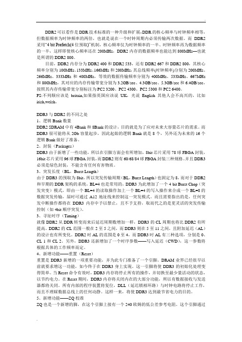
DDR2与DDR3的区别DDR2与DDR3内存参数对比目前,DDR2与DDR3是最主流的两种内存规格,其工作频率为400MHz-1000MHz,由于采用双倍数据速率(Double Data Rate)技术,所以DDR2内存的有效频率为800MHz,最高可达到DDR2-1066甚至DDR2-1200,DDR3内存甚至可达到2133以上的频率。
除了工作频率外,内存另一个重要的参数就是时序,这也是不同品牌和产品之间的差异。
时序表示内存完成一项工作所需要的时间周期,时间越长,则表示执行效率越低。
上图为大家对比的是目前主流标准DDR2与DDR3金士顿内存参数对比,通过对比我们可以发现,在主频方面,DDR3内存是1333MHz明显高于DDR2的800MHz的主频,另外在时序方面DDR3内存也优秀于DDR2内存,还有一个方面就是功耗方面,DDR3工作电压为1.5v低于DDR2的工作电压,也就是说DDR3内存速度全面优秀于上一代DDR2内存,并且耗电更少。
DDR2与DDR3内存的区别还有不少,比如单条内存DDR3内存可以做的更大容量等,我们主要知道DDR3是DDR2的升级版本,其性能不管是速度还是功耗都明显优秀于上一代DDR2产品。
- 1、下载文档前请自行甄别文档内容的完整性,平台不提供额外的编辑、内容补充、找答案等附加服务。
- 2、"仅部分预览"的文档,不可在线预览部分如存在完整性等问题,可反馈申请退款(可完整预览的文档不适用该条件!)。
- 3、如文档侵犯您的权益,请联系客服反馈,我们会尽快为您处理(人工客服工作时间:9:00-18:30)。
Appendix X: Specific SPD’s for DDR2SDRAM(Revision 1.0)1.0 IntroductionThis appendix describes the presence detects for the DDR2 version of the synchronous DRAM modules. These PD’s are those referenced in the SPD standard document for ‘Specific Features’. The following SPD fields will occur in the order presented in section 1.1. Futher descriptions of Bytes 0 and 1 are found in the SPD standard. Further description of Byte 2 is found in Appendix A of the SPD standard. All unused entries wiil be coded as 00h. All unused bits in defined bytes will be coded as 0 except where noted.1.1 Address mapThe following is the SPD address map for DDR2 SDRAM. It describes where the individual LUT-entries will be held in the serial EEPROM.Byte Number Function Described Notes 0Number of Serial PD Bytes written during module production11Total number of Bytes in Serial PD device22Fundamental Memory Type (FPM, EDO, SDRAM, DDR, DDR2…)3Number of Row Addresses on this assembly4Number of Column Addresses on this assembly5Number of DIMM Ranks6Data Width of this assembly7Reserved8Voltage Interface Level of this assembly9SDRAM Cycle time at Maximum Supported CAS Latency (CL), CL=X3 10SDRAM Access from Clock11DIMM configuration type (Non-parity, Parity or ECC)12Refresh Rate/Type3, 4 13Primary SDRAM Width14Error Checking SDRAM Width15Reserved16SDRAM Device Attributes: Burst Lengths Supported17SDRAM Device Attributes: Number of Banks on SDRAM Device3 18SDRAM Device Attributes: CAS Latency3 19Reserved3 20DIMM Type Information3 21SDRAM Module Attributes22SDRAM Device Attributes: General3 23Minimum Clock Cycle at CLX-13 24Maximum Data Access Time (tAC) from Clock at CLX-13 25Minimum Clock Cycle at CLX-23 26Maximum Data Access Time (tAC) from Clock at CLX-23 27Minimum Row Precharge Time (tRP)3 28Minimum Row Active to Row Active delay (tRRD)3 29Minimum RAS to CAS delay (tRCD)3 30Minimum Active to Precharge Time (tRAS)3 31Module Rank Density32Address and Command Input Setup Time Before Clock (tIS)3 33Address and Command Input Hold Time After Clock (tIH)3 34Data Input Setup Time Before Clock(tDS)3Byte Number Function Described Notes 35Data Input Hold Time After Clock (tDH)3 36Write recovery time (tWR)3 37Internal write to read command delay (tWTR)3 38Internal read to precharge command delay (tRTP)3 39Memory Analysis Probe Characteristics40Extension of Byte 41 tRC and Byte 42 tRFC41SDRAM Device Minimum Active to Active/Auto Refresh Time (tRC)3 42SDRAM Device Minimum Auto-Refresh to Active/Auto-Refresh Command Period (tRFC)3 43SDRAM Device Maximum device cycle time (tCKmax)3 44SDRAM Device maximum skew between DQS and DQ signals (tDQSQ)3 45SDRAM Device Mazimum Read DataHold Skew Facktor (tQHS)3 46PLL Relock Time47-xx IDD in SPD(IDD in SPD TG is working to defiene this standard, and a discussion result will be added laterxx-61Reserved62SPD Revision63Checksum for Bytes 0-6264-71Manufacturer’s JEDEC ID Code72Module Manufacturing Location5 73-90Module Part Number5 91-92Module Revision Code5 93-94Module Manufacturing Date5 95-98Module Serial Number99-127Manufacturer’s Specific Data5 128-255Open for customer use1.This will typically be programmed as 128 Bytes.2.This will typically be programmed as 256 Bytes.3.From Datasheet.4.High order bit is Self Refresh “flag”. If set to “1”, the assembly supports self refresh.5.These are optional, in accordance with the JEDEC spec.2.0 Details of each byteByte 0: Number of Bytes Utilized by Module ManufacturerThis field describes the total number of bytes used by the module manufacturer for the SPD data and any (optional) specific supplier information. The byte count includes the fields for all required and optional data.Line #Number SPD Bytes Bit 7Bit 6Bit 5Bit 4Bit 3Bit 2Bit 1Bit 0Hex 0Undefined0000000000 110000000101 220000001002 330000001103 440000010004 550000010105 660000011006 ----------------------1281281000000080 ---------------------------------25425411111110FE 25525511111111FFByte 1: Total Number of Bytes in Serial PD DeviceThis field describes the total size of the serial memory used to hold the Serial Presence Detect data. The fol-lowing lookup table describes the possible serial memory densities (in bytes) along with the corresponding descriptor.Line #Serial Memory Bit 7Bit 6Bit 5Bit 4Bit 3Bit 2Bit 1Bit 0Hex 0Undefined0000000000 12Bytes0000000101 24Bytes0000001002 38Bytes0000001103 416Bytes0000010004 532Bytes0000010105 664Bytes0000011006 7128Bytes0000011107 8256Bytes0000100008 9512Bytes0000100109 101024Bytes000010100A 112048Bytes000010110B 124096Bytes000011000C 138192Bytes000011010D 1416384 Bytes000011100E ----------------------254-11111110FE 255-11111111FFByte 2: Memory TypeThis byte describes the fundamental memory type (or technology) implemented on the module.Line #Fundamental Memory Type Bit 7Bit 6Bit 5Bit 4Bit 3Bit 2Bit 1Bit 0Hex 0Reserved0000000000 1Standard FPM DRAM0000000101 2EDO0000001002 3Pipelined Nibble0000001103 4SDRAM0000010004 5ROM0000010105 6SGRAM DDR0000011006 7SDRAM DDR0000011107 8DDR-II SDRAM0000100008 -----------253TBD11111101FD 254TBD11111110FE 255TBD11111111FFByte 3: Number of Row AddressesThis field describes the Row addressing on the module. bit 0-3 are used to represent the number of row addresses, bit 4-7 are reserved and should be coded as ‘0’Examples of Byte 3 implementation include:Number of RowAddressesModule Organization Device Used Byte 3 Contents13, RA0-RA1232M x 6432M x 160000 110114, RA0-RA1364M x 6464M x 80000 1110Line #Number of RowAddressesBit 7Bit 6Bit 5Bit 4Bit 3Bit 2Bit 1Bit 0Hex0Undefined0000000000 110000000101 220000001002 330000001103 440000010004 550000010105 660000011006 770000011107 880000100008 990000100109 1010000010100A 1111000010110B 1212000011000C 1313000011010D 1414000011100E 1515000011110F -----------25425411111110FE 25525511111111FFByte 4: Number of Column AddressesThis field describes the Column addressing on the module. bit 0-3 are used to represent the number of col-umn addresses, bit 4-7 are reserved and should be coded as ‘0’For example:Number of ColumnAddressesModule Organization Device Used Byte 4 Contents10, CA0-CA932M x 6432M x 160000 101010, CA0-CA964M x 6464M x 80000 1010Line #Number of ColumnAddressesBit 7Bit 6Bit 5Bit 4Bit 3Bit 2Bit 1Bit 0Hex0Undefined0000000000 110000000101 220000001002 330000001103 440000010004 550000010105 660000011006 770000011107 880000100008 990000100109 1010000010100A 1111000010110B 1212000011000C 1313000011010D 1414000011100E 1515000011110F -----------25425411111110FE 25525511111111FFByte 5: Module Attributes - Number of Ranks, Package and HeightThis field describes the number of ranks (Rank: any DRAMs connected to same physical CS) and package on the SDRAM module, and module height. The number of logical banks for the SDRAM device is defined in Byte 17.Bit 7 ~ Bit 5Bit 4Bit 3Bit 2 ~ Bit 0Module Height DRAM Packgage Card on Card# of RanksBit[ 7, 6, 5]000 = less than 25.4mm001 = 25.4mm 010 =g reater t han 25.4mm a nd l ess t han 30 m m011 = 30.0mm100 = 30.5mm101 = greater than 30.5 mm others :reserved 1 = stack0 = planar1 = yes0 = noBit [2, 1, 0] :000 = 1rank001 = 2ranks010 = 3ranks011 = 4 ranks......111 = 8ranksByte 6: Module Data WidthByte 6 is used to designate the module’s data width. For example:If the module’s Data Width is:and Byte 6 is:640100 0000720100 1000Line #Data Width Bit 7Bit 6Bit 5Bit 4Bit 3Bit 2Bit 1Bit 0Hex 000000000000 -----------32320010000020 33330010000121 -----------36360010010024 -----------64640100000040 -----------72720100100048 -----------80800101000050 -----------1281281000000080 -----------1441441001000090 -----------25425411111110FE 25525511111111FFByte 7: ReservedByte 8: Voltage Interface Level of this assemblyThis field describes the module’s voltage interface.Line #Interface Levels Bit 7Bit 6Bit 5Bit 4Bit 3Bit 2Bit 1Bit 0Hex 0TTL/5V tolerant00000000001 LVTTL (not 5V tolerant)0000000101STL1.5V0000001002 2H3SSTL3.3V0000001103 4SSTL2.5V0000010004 5SSTL1.8V0000010105 6TBD0000011006 -----------Byte 9: SDRAM Cycle TimeThis byte defines the minimum cycle time for the SDRAM module at the highest CAS Latency, CAS Latency =X, defined in byte 18. If other CAS latencies are supported, then the associated minimum cycle times are not related in this version of the SPD standard. Byte 9, Cycle time for CAS Latency=X, is split into two nib-bles: the higher order nibble (bits 4-7) designates the cycle time to a granularity of 1ns; the value presented by the lower order nibble (bits 0-3) has a granularity of .1ns and is added to the value designated by the higher nibble. In addition, four lines of the lower order nibble are assigned to support +.25,+.33, +.66 and +.75. For example:If bits 7:4 areand bits 3:0 arethen the total time is:00111101(3ns)+ (.75ns)= 3.75nsByte 9, SDRAM Cycle Time, Subfield A: Whole Nanoseconds (Bits 4-7)Line #Cycle Time Bit 7Bit 6Bit 5Bit 4Bit 3Bit 2Bit 1Bit 0Hex 0A Undefined 00000_1A 1ns 00011_2A 2ns 00102_3A 3ns 00113_4A 4ns 01004_5A 5ns 01015_6A 6ns 01106_7A 7ns 01117_8A 8ns 10008_9A 9ns 10019_10A 10ns 1010A_11A 11ns 1011B_12A 12ns 1100C_13A 13ns 1101D_14A 14ns 1110E_15A 15ns 1111F_-Undefined11111111FFByte 9, SDRAM Cycle Time Subfield B: Tenths of Nanoseconds (Bits 0-3)Line #Cycle Time Bit 7Bit 6Bit 5Bit 4Bit 3Bit 2Bit 1Bit 0Hex 0B +0ns ----0000_01B +.1ns 0001_12B +.2ns 0010_23B +.3ns 0011_34B +.4ns 0100_45B +.5ns 0101_56B +.6ns 0110_67B +.7ns 0111_78B +.8ns 1000_89B +.9ns 1001_910B +.25ns 1010_A 11B +.33ns 1011_B 12B +.66ns 1100_C 13B +.75ns 1101_D ------------Undefined11111111FFSee Subfield Table BSee Subfield Table BByte 10: SDRAM Access from Clock (t AC )This byte defines the maximum clock to data out for the SDRAM module. This is the Clock to data out speci-fication at the highest given CAS Latency specified in byte 18 of this SPD specification. If other CAS latencies are supported, then the associated Maximum Clock Access times are not related in this version of the SPD standard. The byte is split into two nibbles: the higher order nibble (bits 4-7) designate the access time to a granularity of 0.1ns; the value presented by the lower order nibble (bits 0-3) has the granularity of .01ns and is added to the value designated by the higher nibble. For example:if bits 7:4 areand bits 3:0 are then the total time is:00110101(0.3ns)+ (0.05ns)= 0.35nsByte 10: SDRAM Access from Clock, Subfield A: Tenths of Nanoseconds (Bits 4-7)Line #Access from ClockBit 7Bit 6Bit 5Bit 4Bit 3Bit 2Bit 1Bit 0Hex 0A Undefined 00000_1A .1ns 00011_2A .2ns 00102_3A .3ns 00113_4A .4ns 01004_5A .5ns 01015_6A .6ns 01106_7A .7ns 01117_8A .8ns 10008_9A .9ns 10019_10A RFU 1010A_11A -1011--Undefined11111111FFByte 10: SDRAM Access from Clock Subfield B: Hundredths of Nanoseconds (Bits 0-3)Line #Access from ClockBit 7Bit 6Bit 5Bit 4Bit 3Bit 2Bit 1Bit 0Hex 0B +0ns 0000_01B +.01ns 0001_12B +.02ns 0010_23B +.03ns 0011_34B +.04ns 0100_45B +.05ns 0101_56B +.06ns 0110_67B +.07ns 0111_78B +.08ns 1000_89B +.09ns 1001_910B RFU 1010_A 11B –----------Undefined11111111FFSee Subfield BSee Subfield AByte 11: DIMM Configuration TypeThis byte describes the module’s error detection and/or correction scheme.Byte 12: Refresh Rate/TypeThis byte describes the module’s refresh rate.Line #Error Detection/CorrectionBit 7Bit 6Bit 5Bit 4Bit 3Bit 2Bit 1Bit 0Hex 0None 00000000001Parity 00000001012ECC 00000010023TBD 00000011034TBD 00000100045TBD 00000101056TBD 0000011006----------------------Line #Refresh Period Bit 7(Self RefreshFlag)Bit 6Bit 5Bit 4Bit 3Bit 2Bit 1Bit 0Hex 0Normal (15.625 us)00000000001Reduced (.25x)...3.9us 00000001012Reduced (.5x)...7.8us 00000010023Extended (2x)...31.3us 00000011034Extended (4x)...62.5us 00000100045Extended (8x)...125us00000101056TBD 00000110067TBD 0000011107----------------------Byte 13: Primary SDRAM WidthBits 0-7 of this byte indicate the width of the primary data SDRAM. The primary SDRAM is that which is used for data; examples of primary (data) SDRAM widths are x4, x8, x16, and x32. Note that if the module is made with SDRAMs which provide for data and error checking, e.g. x9, x18, and x36, then it is also designated in this field.This table contains examples of SDRAM DIMMModule Width Primary SDRAMWidthError CheckingSDRAM WidthPossible (512Mbbased) ModuleDensityByte 13Contentsx72x8x8512MB0000 1000x72x16x16256MB0001 0000x72x8x161024MB0000 1000Line #SDRAM Data Width Bit 7Bit 6Bit 5Bit 4Bit 3Bit 2Bit 1Bit 0Hex 0Undefined0000000000 110000000101 220000001002 330000001103 440000010004 550000010105 660000011006 770000011107 880000100008 990000100109 1010000010100A 1111000010110B 1212000011000C 1313000011010D 1414000011100E 1515000011110F -----------25425411111110FE 25525511111111FFByte 14: Error Checking SDRAM WidthIf the module incorporates error checking and if the primary data SDRAM does not include these bits — i.e. there are separate error checking SDRAMs — then the error checking SDRAM’s width is expressed in this byte. Bits 0-7 of this byte relate the error checking SDRAM’s width.The following table contains examples of error checking SDRAM widthsModule Width Primary SDRAMWidthError CheckingSDRAM WidthPossible (512Mbbased) ModuleDensityByte 14Contentsx72x8x8512MB0000 1000 x72x16x16256MB0001 0000 x72x8x161024MB0001 0000Line #Error CheckingSDRAM WidthBit 7Bit 6Bit 5Bit 4Bit 3Bit 2Bit 1Bit 0Hex0Undefined0000000000 110000000101 220000001002 330000001103 440000010004 550000010105 660000011006 770000011107 880000100008 990000100109 1010000010100A 1111000010110B 1212000011000C 1313000011010D 1414000011100E 1515000011110F -----------25425411111110FE 25525511111111FFByte 15: ReservedByte 16: SDRAM Device Attributes – Burst Lengths SupportedThis byte describes which various programmable burst lengths are supported by the devices on the module. If the bit is “1”, then that Burst Length is supported on the module; if the bit is “0”, then that Burst Length is not supported by the module.Byte 17: SDRAM Device Attributes – Number of Banks on SDRAM DeviceThis byte details how many banks are on each SDRAM installed onto the module.Bit 7Bit 6Bit 5Bit 4Bit 3Bit 2Bit 1Bit 0TBD TBD TBD TBD Burst Length= 8Burst Length= 4TBD TBD 01 or 01 or 01 = Supported on this assembly, 0 = Not supported on this assembly.Line #Number of BanksBit 7Bit 6Bit 5Bit 4Bit 3Bit 2Bit 1Bit 0Hex 0Undefined0000000000----------------------440000010004-----------880000100008-----------25525511111111FFByte 18: SDRAM Device Attributes – CAS LatencyThis byte describes which of the programmable CAS latencies are acceptable for the module. If the bit is “1”, then that CAS latency is supported on the module; if the bit is “0”, then that CAS latency is not supported by the module.Byte 19: ReservedByte 20: DIMM type informationThis byte describes the DIMM type information of DDR2 SDRAM .Bit 7Bit 6Bit 5Bit 4Bit 3Bit 2Bit 1Bit 0TBD TBD CAS Latency= 5CAS Latency= 4CAS Latency= 3CAS Latency= 2TBD TBD 01 or 01 or 01 or 01 or 01 = Supported on this assembly; 0 = Not supported on this assembly.Bit 7Bit 6Bit 5Bit 4Bit 3Bit 2Bit 1Bit 0TBD TBD Mini-UDIMM (82.0 mm)*Mini-RDIMM (82.0 mm)*Micro-DIMM (45.5 mm)*SO-DIMM (67.6 mm)*Regular UDIMM (133.35 mm)*Regular RDIMM (133.35 mm)*1 or 01 or 01 or 01 or 01 or 01 or 01 = Supported on this assembly; 0 = Not supported on this assembly.* numbers shown are module widthByte 21: SDRAM Modules AttributesThis byte depicts various aspects of the module. It details various unrelated but critical elements pertinent to the module. A given module characteristic is detailed in the designated bit; if the aspect is TRUE, then the bit is “1”. Conversely, if the aspect is FALSE, the designated bit is “0”.Byte 22: SDRAM Device Attributes – GeneralThis byte depicts various aspects of the SDRAMs on the module. It details various unrelated but critical ele-ments pertinent to the SDRAMs. A given SDRAM characteristic is detailed in the designated bit; if the aspect is TRUE, then the bit is “1”. Conversely, if the aspect is FALSE, the designated bit is “0”.Bit 7Bit 6Bit 5Bit 4Bit 3Bit 2Bit 1Bit 0TBD *Analysis probeinstalledTBD FET Switch External Enable TBD TBD TBD TBD 01 or 01 or 01 = Included on this assembly; 0 = Not included on this assembly.* All normal DIMMs will set bit 6 to 0. If bit 6 is set to a 1 this indicates that a memory bus analysis probe is installed in the slot. The BIOS should ensure that Address and Command bus clocks remain turned for that slot and byte 39 may be optionally consulted to determine probe characteristicsBit 7Bit 6Bit 5Bit 4Bit 3Bit 2Bit 1Bit 0TBD TBD TBD TBD TBD TBD TBD Supports Weak Driver 01 or 0Byte 23: Minimum Clock Cycle Time at Reduced CAS Latency, X- 1The highest CAS latency identified in byte 18 is X and the timing values associated with CAS latency ‘X’ are found at byte locations 9 and 10. Byte 23 denotes the minimum cycle time at CAS latency X- 1.For example, if byte 18 denotes CAS latencies of 3 to 4, then X is 4 and X-1 is 3. Byte 23 then denotes the minimum cycle time at CAS latency 3.Byte 23 is split into two nibbles: the higher order nibble (bits 4-7) designate the cycle time to a granularity of 1ns; the value presented by the lower order nibble (bits 0-3) has a granularity of .1ns and is added to the value designated by the higher nibble. In addition, four lines of the lower order nibble are assigned to support +0.25,+.33, +.66 and +.75. For example:if bits 7:4 areand bits 3:0 arethen the total time is00111011(3ns)+ (.75ns)=3.75nsByte 23, SDRAM Minimum Cycle Time @ CL X-1, Subfield A: Whole Nanoseconds (Bits 4-7)Line #Access from ClockBit 7Bit 6Bit 5Bit 4Bit 3Bit 2Bit 1Bit 0Hex 0A Undefined 00000_1A 1ns/16ns 00011_2A 2ns/17ns 00102_3A 3ns 00113_4A 4ns 01004_5A 5ns 01015_6A 6ns 01106_7A 7ns 01117_8A 8ns 10008_9A 9ns 10019_10A 10ns 1010A_11A 11ns 1011B_12A 12ns 1100C_13A 13ns 1101D_14A 14ns 1110E_15A15ns1111F_Byte 23, SDRAM Minimum Cycle Time @ CL X-1, Subfield B: Tenths of Nanoseconds (Bits 0-3)Line #Access from ClockBit 7Bit 6Bit 5Bit 4Bit 3Bit 2Bit 1Bit 0Hex 0B +0ns 0000_01B +.1ns 0001_12B +.2ns 0010_23B +.3ns 0011_34B +.4ns 0100_45B +.5ns 0101_56B +.6ns 0110_67B +.7ns 0111_78B +.8ns 1000_89B +.9ns 1001_910B +.25ns 1010_A 11B +.33ns 1011_B 12B +.66ns 1100_C 13B +.75ns 1101_D -..........-Undefined11111111FFSee Subfield BSee Subfield AByte 24: Maximum Data Access Time (t AC ) from Clock at CL X- 1The highest CAS latency identified in byte 18 is X. Byte 23 denotes the maximum access time from Clock at CAS latency X- 1.For example, if byte 18 denotes supported CAS latencies of 3 to 4, then X is 4 and X-1 is 3. Byte 24 then denotes the maximum clock access time from CK at CAS latency 3.Byte 24 is split into two nibbles: the higher order nibble (bits 4-7) designate the access time to a granularity of 0.1ns; the value presented by the lower order nibble (bits 0-3) has the granularity of .01ns and is added to the value designated by the higher nibble. For example:if bits 7:4 are and bits 3:0 are then the total time is:00110101(0.3 ns)+ (0.05 ns)= 0.35 nsByte 24: SDRAM Access from Clock @ X-1, Subfield A: Tenths of Nanoseconds (Bits 4-7)Line #Access from ClockBit 7Bit 6Bit 5Bit 4Bit 3Bit 2Bit 1Bit 0Hex 0A Undefined 00000_1A .1ns 00011_2A .2ns 00102_3A .3ns 00113_4A .4ns 01004_5A .5ns 01015_6A .6ns 01106_7A .7ns 01117_8A .8ns 10008_9A .9ns 10019_10A RFU 1010A_11A -1011--Undefined11111111FFByte 24: SDRAM Access from Clock @ X-1, Subfield B: Hundredths of Nanoseconds (Bits 0-3)Line #Access from ClockBit 7Bit 6Bit 5Bit 4Bit 3Bit 2Bit 1Bit 0Hex 0B +0ns 0000_01B +.01ns 0001_12B +.02ns 0010_23B +.03ns 0011_34B +.04ns 0100_45B +.05ns 0101_56B +.06ns 0110_67B +.07ns 0111_78B +.08ns 1000_89B +.09ns 1001_910B RFU 1010_A 11B –----------Undefined11111111FFSee Subfield BSee Subfield AByte 25: Minimum Clock Cycle Time at CL X-2The highest CAS latency identified in byte 18 is X. Byte 25 denotes the minimum cycle time at CAS latency X-2.For example, if byte 18 denotes CAS latencies of 3 to 5, then X is 5 and X-2 is 3. Byte 25 then denotes the minimum cycle time at CAS latency 3.Byte 25 is split into two nibbles: the higher order nibble (bits 4-7) designates the cycle time to a granularity of 1ns; the value presented by the lower order nibble (bits 0-3) has a granularity of .1ns and is added to the value designated by the higher order nibble. In addition, four lines of the lower order nibble are assigned to support +0.25,+.33, +.66 and +.75. For example:if bits 7:2 areand bits 1:0 arethen the total time is00111011(3 ns)+ (.75 ns)= 3.75 nsByte 25, SDRAM Minimum Cycle Time @ CL X-2, Subfield A: Whole Nanoseconds (Bits 4-7)Line #Access from ClockBit 7Bit 6Bit 5Bit 4Bit 3Bit 2Bit 1Bit 0Hex 0A Undefined 00000_1A 1ns/16ns 00011_2A 2ns/17ns 00102_3A 3ns 00113_4A 4ns 01004_5A 5ns 01015_6A 6ns 01106_7A 7ns 01117_8A 8ns 10008_9A 9ns 10019_10A 10ns 1010A_11A 11ns 1011B_12A 12ns 1100C_13A 13ns 1101D_14A 14ns 1110E_15A15ns1111F_Byte 25, SDRAM Minimum Cycle Time @ CL X-2, Subfield B: Tenths of Nanoseconds (Bits 0-3)Line #Access from ClockBit 7Bit 6Bit 5Bit 4Bit 3Bit 2Bit 1Bit 0Hex 0B +0ns 0000_01B +.1ns 0001_12B +.2ns 0010_23B +.3ns 0011_34B +.4ns 0100_45B +.5ns 0101_56B +.6ns 0110_67B +.7ns 0111_78B +.8ns 1000_89B +.9ns 1001_910B +.25ns 1010_A 11B +.33ns 1011_B 12B +.66ns 1100_C 13B +.75ns 1101_D -..........-Undefined11111111FFSee Subfield BSee Subfield AByte 26: Maximum Data Access Time (t AC ) from Clock at CL X-2The highest CAS latency identified in byte 18 is X. Byte 26 denotes the maximum access time from Clock at CAS latency X-2.For example, if byte 18 denotes supported CAS latencies of 3 to 5, then X is 5 and X-2 is 3. Byte 26 then denotes the maximum data access time from CK at CAS latency 3.Byte 26 is split into two nibbles: the higher order nibble (bits 4-7) designate the access time to a granularity of 0.1ns; the value presented by the lower order nibble (bits 0-3) has the granularity of .01ns and is added to the value designated by the higher nibble. For example:if bits 7:4 areand bits 3:0 are then the total time is:00110101(0.3ns)+ (0.05ns)= 0.35nsByte 26: SDRAM Access from Clock @ CL = X-2, Subfield A: Tenths of Nanoseconds (Bits 4-7)Line #Access from ClockBit 7Bit 6Bit 5Bit 4Bit 3Bit 2Bit 1Bit 0Hex 0A Undefined 00000_1A .1ns 00011_2A .2ns 00102_3A .3ns 00113_4A .4ns 01004_5A .5ns 01015_6A .6ns 01106_7A .7ns 01117_8A .8ns 10008_9A .9ns 10019_10A RFU 1010A_11A -1011--Undefined11111111FFByte 26: SDRAM Access from Clock @ CL = X-2, Subfield B: Hundredths of Nanoseconds (Bits 0-3)Line #Access from ClockBit 7Bit 6Bit 5Bit 4Bit 3Bit 2Bit 1Bit 0Hex 0B +0ns 0000_01B +.01ns 0001_12B +.02ns 0010_23B +.03ns 0011_34B +.04ns 0100_45B +.05ns 0101_56B +.06ns 0110_67B +.07ns 0111_78B +.08ns 1000_89B +.09ns 1001_910B RFU 1010_A 11B –----------Undefined11111111FFSee Subfield BSee Subfield AByte 27: Minimum Row Precharge Time (t RP )Byte 27 is used to designate the module’s minimum Row Precharge time.Byte 27 is split into two pieces: the higher order bits (bits 2-7) designate the time to a granularity of 1ns; the value presented by the lower order bits (bits 0-1) has a granularity of .25ns and is added to the value desig-nated by the higher bits. For example:if bits 7:2 are and bits 1:0 arethen the total time is001111(15ns)00+(0.0ns)= 15.0ns 010010(18ns)11+(.75ns)= 18.75nsByte 27, SDRAM Minimum t RP Time, Subfield A: Whole Nanoseconds (Bits 2-7)Nanoseconds Bit 7Bit 6Bit 5Bit 4Bit 3Bit 2Bit 1Bit 0Undefined 0000001ns 0000012ns 0000103ns 0000114ns 0001005ns 0001016ns 0001107ns 0001118ns 0010009ns 00100110ns 001010::::::::::::::61ns 11110162ns 11111063ns111111Byte 27, SDRAM Minimum t RP Time, Subfield B: Quarters of Nanoseconds (Bits 0-1)Access from ClockBit 7Bit 6Bit 5Bit 4Bit 3Bit 2Bit 1Bit 0+0ns 00+.25ns 01+.50ns 10+.75ns11See Subfield B See Subfield AByte 28: Minimum Row Active to Row Active Delay (t RRD )This field describes the minimum required delay between different row activations.Byte 28 is split into two pieces: the higher order bits (bits 2-7) designate the time to a granularity of 1ns; the value presented by the lower order bits (bits 0-1) has a granularity of .25ns and is added to the value desig-nated by the higher bits. For example:if bits 7:2 are and bits 1:0 arethen the total time is000111(7ns)10+(0.5ns)= 7.5ns 001010(10ns)00+(0.0ns)= 10nsByte 28, SDRAM Minimum t RRD Time, Subfield A: Whole Nanoseconds (Bits 2-7)Nanoseconds Bit 7Bit 6Bit 5Bit 4Bit 3Bit 2Bit 1Bit 0Undefined 0000001ns 0000012ns 0000103ns 0000114ns 0001005ns 0001016ns 0001107ns 0001118ns 0010009ns 00100110ns 001010::::::::::::::61ns 11110162ns 11111063ns111111Byte 28, SDRAM Minimum t RRD Time, Subfield B: Quarters of Nanoseconds (Bits 0-1)Access from ClockBit 7Bit 6Bit 5Bit 4Bit 3Bit 2Bit 1Bit 0+0ns 00+.25ns 01+.50ns 10+.75ns11See Subfield B See Subfield AByte 29: Minimum RAS to CAS Delay (t RCD )This byte describes the minimum delay required between assertions of RAS and CAS.Byte 29 is split into two pieces: the higher order bits (bits 2-7) designate the time to a granularity of 1ns; the value presented by the lower order bits (bits 0-1) has a granularity of .25ns and is added to the value desig-nated by the higher bits. For example:if bits 7:2 are and bits 1:0 arethen the total time is001111(15ns)00+(0.0ns)= 15.0ns 010010(18ns)11+(.75ns)= 18.75nsByte 29, SDRAM Minimum t RCD Time, Subfield A: Whole Nanoseconds (Bits 2-7)Nanoseconds Bit 7Bit 6Bit 5Bit 4Bit 3Bit 2Bit 1Bit 0Undefined 0000001ns 0000012ns 0000103ns 0000114ns 0001005ns 0001016ns 0001107ns 0001118ns 0010009ns 00100110ns 001010::::::::::::::61ns 11110162ns 11111063ns111111Byte 29, SDRAM Minimum t RCD Time, Subfield B: Quarters of Nanoseconds (Bits 0-1)Access from ClockBit 7Bit 6Bit 5Bit 4Bit 3Bit 2Bit 1Bit 0+0ns 00+.25ns 01+.50ns 10+.75ns11See Subfield B See Subfield AByte 30: Minimum Active to Precharge Time (t RAS)This byte identifies the minimum active to precharge time.Minimum Active toBit 7Bit 6Bit 5Bit 4Bit 3Bit 2Bit 1Bit 0Hex Precharge Time (ns)00000 Undefined00001000000010120000001002....................25000110011926000110101A27000110111B28000111001C29000111011D30000111101E31000111111F320010000020330010000121340010001022350010001123360010010024....................127011111117F1281000000080....................25411111110FE25511111111FF。