NI_USB-6218
NI USB-6002低成本DAQUSB设备规格表说明书
SPECIFICATIONSNI USB-6002Low-Cost DAQ USB DeviceThe following specifications are typical at 25 °C, unless otherwise noted. For more information about the NI USB-6002, refer to the NI USB-6001/6002/6003 User Guide available at /manuals.Analog InputNumber of channelsDifferential4....................................................................Single-ended8....................................................................ADC resolution16-bit ............................................................................Maximum sample rate (aggregate)50 kS/s ............................................................................Converter type Successive approximation ............................................................................ ............................................................................AI FIFO2,047 samplesTrigger sources Software, PFI 0, PFI 1 ........................................................................................................................................................Input range±10 VWorking voltage±10 V ............................................................................Overvoltage protectionPowered-on±30 V....................................................................Powered-off±20 V....................................................................Input impedance>1 GΩ............................................................................Input bias current±200 pA ............................................................................Absolute accuracy....................................................................Typical at full scale 6 mV26 mVMaximum over temperature,....................................................................full scaleSystem noise0.4 mVrms.................................................................... ............................................................................DNL16-bit, no missing codesINL±1.8 LSB ............................................................................CMRR56 dB (DC to 5 kHz) ............................................................................Bandwidth300 kHz ............................................................................Analog OutputAnalog outputs2 ............................................................................DAC resolution16-bit ............................................................................Output range±10 V ............................................................................Maximum update rate 5 kS/s simultaneous per channel, hardware-............................................................................timedAO FIFO2,047 samples ............................................................................ ............................................................................Trigger sources Software, PFI 0, PFI 1Output current drive±5 mA ............................................................................Short circuit current±11 mA ............................................................................Slew rate 3 V/μs ............................................................................Output impedance0.2 Ω............................................................................2| | NI USB-6002 SpecificationsAbsolute accuracy (no load)Typical at full scale8.6 mV....................................................................Maximum over temperature, full scale32 mV....................................................................DNL16-bit, no missing codes ............................................................................INL±4 LSB ............................................................................Power-on state0 V ............................................................................ ............................................................................Startup glitch-7 V for 10 µsTimebaseNote The following specifications apply to the sampling accuracy for hardware-timed analog input and analog output.Timebase frequency80 MHz ............................................................................Timebase accuracy±100 ppm ............................................................................ ............................................................................Timing resolution12.5 nsDigital I/O13 digital lines....................................................................Port 08 linesPort 1 4 lines....................................................................Port 2 1 lines....................................................................FunctionP0.<0..7>Static digital input/output....................................................................P1.0Static digital input/output........................................................................................................................................P1.1/PFI 1Static digital input/output, counter source ordigital triggerNI USB-6002 Specifications| © National Instruments| 3....................................................................P1.<2..3>Static digital input/outputP2.0/PFI 0Static digital input/output, counter source or ....................................................................digital triggerDirection control Each channel individually programmable as ............................................................................input or outputOutput driver type Each channel individually programmable as ............................................................................open collector or active driveAbsolute maximum voltage range-0.3 V to 5. 5 V with respect to D GND ............................................................................Pull-down resistor47.5 kΩ to D GND ............................................................................Power-on state Input ............................................................................Digital InputInput voltage range (powered on)0 to 5 V ............................................................................ ............................................................................Input voltage range (powered off)0 to 3.3 VInput voltage protection±20 V on two lines per port (maximum of five ............................................................................lines for all ports) for up to 24 hours Caution Do not leave a voltage above 3.3 V connected on any DIO line forextended periods of time when the device is powered off. This may lead to long termreliability issues. ............................................................................Minimum V IH 2.3 VMaximum V IL0.8 V ............................................................................Maximum input leakage currentAt 3.3 V0.8 mA....................................................................At 5 V 4.5 mA....................................................................Digital Output (Active Drive)Maximum V OL (4 mA)0.7 V ............................................................................Maximum V OL (1 mA)0.2 V ............................................................................Minimum V OH (4 mA) 2.1 V ............................................................................Minimum V OH (1 mA) 2.8 V ............................................................................ ............................................................................Maximum V OH 3.6 VMaximum output current per line±4 mA ............................................................................4| | NI USB-6002 SpecificationsDigital Output (Open Collector) ............................................................................Maximum V OL (4 mA)0.8 VMaximum V OL (1 mA)0.2 V ............................................................................Note Minimum Vdependent on user-provided pull-up resistor and voltagesource. Recommended pull-up resistor is 1 kΩ.Using a 1 kΩ pull-up resistor and 5 V voltagesource:Minimum V OH 3.5 V....................................................................Typical V OH 4.5 V....................................................................Maximum output (sinking) current per line-4 mA ............................................................................ ............................................................................Maximum pull-up voltage 5 VMaximum leakage currentAt 3.3 V0.8 mA........................................................................................................................................At 5 V 4.5 mACounterNumber of counters1 ............................................................................Resolution32-bit ............................................................................Counter measurements Edge counting, rising or falling ............................................................................Counter direction Count up ............................................................................ ............................................................................Counter source PFI 0 or PFI 1Maximum input frequency 5 MHz ............................................................................Minimum high pulse width100 ns ............................................................................ ............................................................................Minimum low pulse width100 nsNI USB-6002 Specifications| © National Instruments| 5+5 V Power SourceOutput voltage+5 V, ±3% ............................................................................Maximum current150 mA ............................................................................Overcurrent protection200 mA ............................................................................Short circuit current50 mA ............................................................................Overvoltage protection±20 V ............................................................................Bus InterfaceUSB specification USB Full Speed ............................................................................ ............................................................................USB bus speed12 Mb/sPhysical CharacteristicsDimensionsWithout screw terminal connector plugs75.4 mm × 86.2 mm × 23.6 mm, (2.97 in. ×....................................................................3.40 in. × 0.93 in.)With screw terminal connector plugs93.2 mm × 86.2 mm × 23.6 mm, (3.67 in. ×....................................................................3.40 in. × 0.93 in.)6| | NI USB-6002 SpecificationsFigure 1. NI USB-6002 DimensionsWeightWithout screw terminal connector plugs83 g (2.93 oz)....................................................................With screw terminal connector plugs105 g (3.70 oz)....................................................................I/O connectors: USB Micro-B receptacle, (1)16-position screw terminal plugsScrew-terminal wiring 1.31 to 0.08 mm2 (16 to 28 AWG)....................................................................Torque for screw terminals0.22 - 0.25 N · m (2.0 - 2.2 lb. · in.)....................................................................If you need to clean the module, wipe it with a dry towel.EnvironmentalTemperature (IEC 60068-2-1 andIEC 60068-2-2)Operating0 to 45 °C....................................................................Storage-40 to 85 °C....................................................................Humidity (IEC 60068-2-56)Operating 5 to 95% RH, noncondensing....................................................................Storage 5 to 90% RH, noncondensing....................................................................NI USB-6002 Specifications| © National Instruments| 7Pollution Degree (IEC 60664)2 ............................................................................Maximum altitude2,000 m ............................................................................Indoor use only.SafetyThis product meets the requirements of the following standards of safety for electrical equipment for measurement, control, and laboratory use:•IEC 61010-1, EN 61010-1•UL 61010-1, CSA 61010-1Note For UL and other safety certifications, refer to the product label or the OnlineProduct Certification section.Electromagnetic CompatibilityThis product meets the requirements of the following EMC standards for sensitive electrical equipment for measurement, control, and laboratory use:•EN 61326-1 (IEC 61326-1): Class A emissions; Basic immunity•EN 55011 (CISPR 11): Group 1, Class A emissions•EN 55022 (CISPR 22): Class A emissions•EN 55024 (CISPR 24): Immunity•AS/NZS CISPR 11: Group 1, Class A emissions•AS/NZS CISPR 22: Class A emissions•FCC 47 CFR Part 15B: Class A emissions•ICES-001: Class A emissionsNote In the United States (per FCC 47 CFR), Class A equipment is intended foruse in commercial, light-industrial, and heavy-industrial locations. In Europe,Canada, Australia, and New Zealand (per CISPR 11) Class A equipment is intendedfor use only in heavy-industrial locations.Note Group 1 equipment (per CISPR 11) is any industrial, scientific, or medicalequipment that does not intentionally generate radio frequency energy for thetreatment of material or inspection/analysis purposes.Note For EMC declarations and certifications, and additional information, refer tothe Online Product Certification section.8| | NI USB-6002 SpecificationsCE ComplianceThis product meets the essential requirements of applicable European Directives, as follows:•2006/95/EC; Low-V oltage Directive (safety)•2004/108/EC; Electromagnetic Compatibility Directive (EMC)Online Product CertificationTo obtain product certifications and the DoC for this product, visit /certification, search by model number or product line, and click the appropriate link in the Certification column. Environmental ManagementNI is committed to designing and manufacturing products in an environmentally responsible manner. NI recognizes that eliminating certain hazardous substances from our products is beneficial to the environment and to NI customers.For additional environmental information, refer to the Minimize Our Environmental Impact web page at /environment. This page contains the environmental regulations and directives with which NI complies, as well as other environmental information not included in this document.Waste Electrical and Electronic Equipment (WEEE) EU Customers This symbol indicates that waste products should be disposed ofseparately from municipal household waste according toWEEE Directive 2002/96/EC of the European Parliament and the Council on wasteelectrical and electronic equipment (WEEE). All products at the end of their lifecycle must be sent to a WEEE collection and recycling center. Proper WEEEdisposal reduces environmental impact and the risk to human health due topotentially hazardous substances used in such equipment. Your cooperation inproper WEEE disposal will contribute to the effective usage of natural resources. Forinformation about the available collection and recycling scheme in a particularcountry, go to /environment/weee.电子信息产品污染控制管理办法(中国RoHS)中国客户National Instruments符合中国电子信息产品中限制使用某些有害物质指令(RoHS)。
超低价的META工具RFtool功能的使用(中文版)

META工具软件RFTool功能的使用1.简述1.1工具介绍META(Mobile Engineering Testing Architecture)是在MTK平台中用于测试、校准、调试手机的一个开发工具,本文主要介绍其射频工具RFTool的使用方法,便于在生产维修中对手机的射频性能进行调整。
1.2 系统配置软件环境●MS Windows ME, 98, 2000 or XPThe following driver and library are needed for META factory:●NI (National Instruments) GPIB-USB driver (The driver is bundled with NI GPIB-USB device) or Agilent GPIB-USB driver.硬件环境●Generic Pentium III or above PC●Agilent 8960 or R&S CMU 200The following hardware is needed for META factory●NI or Agilent GPIB-USB device●Agilent 661x or Agilent 663x2 series power supply1.3 META的安装执行“setup.exe”进行安装,请根据安装步骤提示来进行安装,如图1-3图1图2图32.RF Tool的使用主要介绍RF Tool的PM、TX level and profile、Continuous TX功能2.1 软件的设置2.1.1打开META,先对软件的使用作相应的配置,包括串口、基带芯片型号、波特率等关键参数。
目前使用的基带芯片主要有6205B、6218,后续还会有6219,使用前根据手机的基带芯片选择正确的型号,否则使用工具软件。
图42.1.2打开数据库文件(文件名一般为DataBase..),用于调出手机的参数,注意数据库文件必须跟手机的软件版本对应,开发中心在下发新版软件时候会包括该版软件的数据库文件。
NI USB-622x、625x、628x OEM User Guide
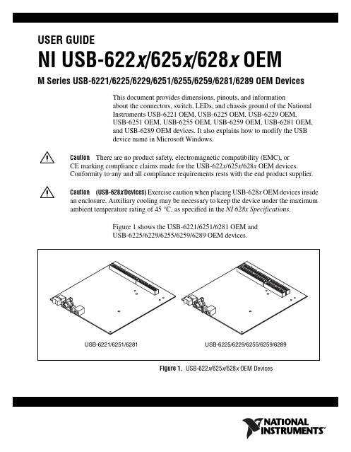
USER GUIDENI USB-622x /625x /628x OEMM Series USB-6221/6225/6229/6251/6255/6259/6281/6289 OEM DevicesThis document provides dimensions, pinouts, and informationabout the connectors, switch, LEDs, and chassis ground of the National Instruments USB-6221 OEM, USB-6225 OEM, USB-6229 OEM,USB-6251 OEM, USB-6255 OEM, USB-6259 OEM, USB-6281 OEM, and USB-6289 OEM devices. It also explains how to modify the USB device name in Microsoft Windows.CautionThere are no product safety, electromagnetic compatibility (EMC), orCE marking compliance claims made for the USB-622x /625x /628x OEM devices. Conformity to any and all compliance requirements rests with the end product supplier.Caution(USB-628x Devices) Exercise caution when placing USB-628x OEM devices insidean enclosure. Auxiliary cooling may be necessary to keep the device under the maximum ambient temperature rating of 45 °C, as specified in the NI 628x Specifications .Figure 1 shows the USB-6221/6251/6281 OEM and USB-6225/6229/6255/6259/6289 OEM devices.Figure 1. USB-622x /625x /628xOEM DevicesRefer to the NI 622x Specifications document for USB-6221/6225/6229specifications, the NI 625x Specifications document forUSB-6251/6255/6259 specifications, and the NI 628x Specificationsdocument for USB-6281/6289 specifications. Refer to the M Series UserManual for more information about USB-622x/625x/628x devices.You can find all documentation at /manuals. DimensionsFigure2 shows the dimensions of the USB-6221/6251/6281 OEM device. NI USB-622x/625x/628x OEM User Figure 2. USB-6221/6251/6281 OEM Dimensions in Inches (Millimeters)© National Instruments Corporation3NI USB-622x/625x/628x OEM User GuideFigure3 shows the dimensions of the USB-6225/6229/6255/6259/6289OEM device.Figure 3. USB-6225/6229/6255/6259/6289 OEM Dimensions in Inches (Millimeters) NI USB-622x/625x/628x OEM User I/O Connector PinoutsFigures4 through9 show the connector pinouts for the USB-6221 OEM,USB-6225 OEM, USB-6229 OEM, USB-6251 OEM, USB-6255 OEM,USB-6259 OEM, USB-6281 OEM, and USB-6289 OEM devices.Refer to the M Series User Manual at /manuals for moreinformation about USB-622x/625x/628x signals and how to connect them.© National Instruments Corporation5NI USB-622x/625x/628x OEM User GuideFigure 4. USB-6221 OEM Connector PinoutNI USB-622x/625x/628x OEM User Figure 5. USB-6225 OEM Connector Pinout© National Instruments Corporation7NI USB-622x/625x/628x OEM User GuideFigure 6. USB-6229 OEM Connector PinoutNI USB-622x/625x/628x OEM User Figure 7. USB-6251/6281 OEM Connector Pinout© National Instruments Corporation9NI USB-622x/625x/628x OEM User GuideFigure 8. USB-6255 OEM Connector PinoutNI USB-622x/625x/628x OEM User Figure 9. USB-6259/6289 OEM Connector PinoutDefault Counter/Timer PinoutsBy default, NI-DAQmx routes the counter/timer inputs and outputs to thePFI pins, shown in Table1.Table 1. NI-DAQmx Default Counter/Timer PinsCounter/Timer Signal Default Terminal NameCTR 0 SRC PFI 8CTR 0 GATE PFI 9CTR 0 AUX PFI 10CTR 0 OUT PFI 12CTR 0 A PFI 8CTR 0 Z PFI 9CTR 0 B PFI 10CTR 1 SRC PFI 3CTR 1 GATE PFI 4CTR 1 AUX PFI 11CTR 1 OUT PFI 13CTR 1 A PFI 3CTR 1 Z PFI 4CTR 1 B PFI 11FREQ OUT PFI 14Attaching External LEDsUSB-622x/625x/628x OEM devices have two LEDs that reflect the devicestate. The green READY LED indicates when the device is powered on andconfigured as a USB device. The yellow ACTIVE LED indicates USB busactivity.Three connectors on the device allow you to connect an external LEDcircuit to the device, as shown in Figure10. To connect an external READYLED, use E1 as the positive connection (+3.3 V) and E2 as the negativeconnection. To connect an external ACTIVE LED, use E1 as the positiveconnection and E3 as the negative connection. E1 is current limited witha100 Ω resistor to the 3.3V internal supply. This configuration limitsthe current to approximately 16mA into a single external LED orapproximately 8 mA each when both LEDs are lit. You also can limit thiscurrent further by using external resistors, also shown in Figure10.Figure 10. Schematic for External LED CircuitsPower SwitchThe power switch on the USB-622x/625x/628x OEM device powers thedevice on and off. Figure11 shows the pins on the power switch andcircuitry.Figure 11. Schematic for the Power SwitchPin1, VDC In, is connected to VDC through the fuse (reference designatorXF1). The VDC is the voltage provided by the power supply through thepower connector (reference designator J4/J6/J81) and must be 11–30VDC,20W.Pin2, VDC Out, provides power to the circuitry on the device. When theswitch is in the On position, the VDC power supply from pin1 is routed topin2.Pin3, 100 kΩ to Ground, connects pin2 to ground through a 100kΩresistor when the switch is in the Off position.1 The power connector is designated as J4 on USB-6225/6255 OEM devices, J6 on USB-6221/6229 OEM devices, and J8 on USB-6251/6259/6281/6289 OEM devices.Connecting the USB-622x /625x /628x OEM Device to Your ChassisThe USB-622x /625x /628x OEM device includes several plated mounting holes that are designed for customer grounded connections, as shown in Figure 12.CautionDo not use the holes labeled A in Figure 12 as mounting holes.Figure 12. Customer Mounting Holes (USB-6225/6229/6255/6259/6289OEM Shown)Caution(USB-628x Devices) Exercise caution when placing USB-628x OEM devices insidean enclosure. Auxiliary cooling may be necessary to keep the device under the maximum ambient temperature rating of 45 °C, as specified in the NI 628x Specifications.Replacing FusesUSB-622x /625x /628x OEM devices have a replaceable T 2A 250V (5×20mm) fuse that protects the device from overcurrent through the power connector.(USB-628x Devices Only) USB-628x OEM devices also have a replaceableF 2A 125V fuse that protects the device from overcurrent through the +5 V terminal(s).Replacement fuse information can be found in Table 2. To replace a broken fuse in USB-622x /625x /628x OEM devices, complete the following steps.1.Power down and unplug the device.2.Replace the broken fuse while referring to Figure 13 for the fuse locations.Figure 13. USB-622x /625x /628x OEM Fuse Locations1T 2A 250V (5 x 20 mm) F us e2F 2A 125V F us e on U S B-628x OEM DevicesDevice ComponentsTable2 contains information about the components used for interfacingand interacting with the USB-622x/625x/628x OEM device.Table 2. USB-622x/625x/628x OEM ComponentsComponent Reference Designator(s) on PCB Manufacturer Manufacturer Part NumberLEDs DS1Dialight553-033234-pin connectors(USB-6221/6251/6281 OEM) J13M N2534-6002RB(USB-6225/6229/6255/6259/6289OEM) J1, J250-pin connectors(USB-6221/6251/6281 OEM) P13M N2550-6002UB(USB-6225/6229/6255/6259/6289OEM) P1, P2USB connector J3AMP787780-1 Power connector(USB-6221/6229OEM) J6Switchcraft722RA(USB-6225/6255OEM) J4(USB-6251/6259/6281/6289OEM) J8Power switch SW1ITT Industries,CannonE101J1A3QE2 T 2A 250V fuse XF1Littelfuse218.002XPF 2A 125V fuse(USB-6281/6289OEM) F1Littelfuse045300268-pin connectors*(USB-6221 OEM) J8Honda PCS-E68RLMD1+ (USB-6225/6229/6255 OEM) J7, J8(USB-6251/6281OEM) J7(USB-6259/6289OEM) J6, J7* Optional mass termination connectors. These are not populated by default.Modifying the USB Device Name in Microsoft WindowsYou can change how the USB-622x/625x/628x OEM device name appearswhen users install the device in both the Found New Hardware Wizard thatappears when the device is initially installed and in the Windows DeviceManager.Windows Vista/XP UsersFigure14 depicts how a USB-6251 OEM device name appears in theFound New Hardware Wizard and Windows Device Manager.Figure 14. USB-6251 OEM Device in the Found New Hardware Wizard andDevice Manager (Windows Vista/XP)To modify the device name in the Found New Hardware Wizard andWindows Device Manager in Microsoft Windows Vista/XP, complete thefollowing steps.Note You must have NI-DAQmx 8.7 or later installed on your PC.1.Locate the OEM x.inf file in the y:\WINDOWS\inf\ directory,where x is the random number assigned to the INF file by Windows,and y:\is the root directory where Windows is installed.NoteNew security updates to Microsoft Vista and NI-DAQ 8.6 or later create random INF files for NI hardware. Windows assigns random file numbers to all INF files, which causes the user to search through several INF files until the correct file is located.If you want to revert back, save a copy of this file as OEM x _original.inf in a different location.2.Edit the device INF file by opening OEM x .inf with a text editor. At the bottom of this file are the descriptors where Windows looks to identify the device. Locate the two lines of text that contain in quotes the descriptors for the device name you are modifying. Change the descriptor on both lines to the new device name, as shown in Figure 15.Figure 15. INF File Descriptors Changed to “My Device” (Windows Vista/XP)3.Save and close the INF file.4.Go to the Windows Device Manager.(Windows Vista) In the Device Manager, notice that the OEM device now appears as My Device , as shown in Figure 16.(Windows XP) In the Device Manager, right-click the OEM device underData Acquisition Devices, and select Uninstall . Power down the OEMdevice and disconnect the USB cable from your PC.Original FileModified FileWhen you reconnect and power on the device, it appears as My Device inthe Found New Hardware Wizard and Windows Device Manager, as shownin Figure16.Note When the device is initially installed, the Windows alert message may display the following: Found New Hardware: M Series USB 62xx (OEM). This message appears for a few seconds until the custom name appears and the Found New Hardware Wizard is launched. This alert message device name cannot be changed.Figure 16. “My Device” in the Found New Hardware Wizard andDevice Manager(Windows Vista/XP)Note Modifying the INF file will not change the USB-622x/625x/628x OEM device name in Measurement & Automation Explorer (MAX).© National Instruments Corporation 21NI USB-622x/625x/628x OEM User GuideWindows 2000 UsersFigure 17 depicts how a USB-6251 OEM device name appears in theFound New Hardware Wizard and Windows Device Manager.Figure 17. USB-6251 OEM Device in the Found New Hardware Wizard andDevice Manager (Windows 2000)To modify the device name in the Found New Hardware Wizard andWindows Device Manager in Windows 2000, complete the following steps.Note You must have NI-DAQmx 8.7 or later installed on your PC.1.Locate the nimioxsu.inf file in the x :\WINNT\inf\ directory,where x :\ is the root directory where Windows is installed.If you want to revert back, save a copy of this file asnimioxsu_original.infin a different location.2.Edit the device INF file by opening nimioxsu.inf with a text editor.At the bottom of this file are the descriptors where Windows looks toidentify the device. Locate the two lines of text that contain in quotesthe descriptors for the device name you are modifying. Change thedescriptor on both lines to the new device name, as shown in Figure18.Original FileModified FileFigure 18. INF File Descriptors Changed to “My Device” (Windows 2000)3.Save and close the INF file.4.Go to the Windows Device Manager, right-click the OEM device underData Acquisition Devices, and select Uninstall.5.Power down the OEM device and disconnect the USB cable fromyour PC.NI USB-622x/625x/628x OEM User National Instruments, NI, , and LabVIEW are trademarks of National Instruments Corporation.Refer to the Terms of Use section on /legal for more information about NationalInstruments trademarks. Other product and company names mentioned herein are trademarks or tradenames of their respective companies. For patents covering National Instruments products, refer to theappropriate location: Help»Patents in your software, the patents.txt file on your media, or/patents .© 2006–2008 National Instruments Corporation. All rights reserved.371910E-01Jun08When you reconnect and power on the device, it appears as My Device inthe Found New Hardware Wizard and Windows Device Manager, as shownin Figure 19.Note When the device is initially installed, the Windows alert message may display the following: Found New Hardware: M Series USB 62xx (OEM). This message appears for a few seconds until the custom name appears and the Found New Hardware Wizard is launched. This alert message device name cannot be changed.Figure 19. “My Device” in the Found New Hardware Wizard andDevice Manager (Windows 2000)Note Modifying the INF file will not change the USB-622x /625x /628x OEM device namein Measurement & Automation Explorer (MAX).。
NI USB-6216 USB多功能I O设备产品规范说明书
产品规范USB-6216隔离16 AI(16位、400 kS/s)、2 AO (250 kS/s)、最高32 DIO USB 多功能I/O设备这些产品规范适用于USB-6216 BNC、USB-6216 Mass终端和USB-6216弹簧端子。
定义担保产品规范给出了型号在规定操作条件下的性能,其中内容涵盖于型号质量担保中。
下列特性产品规范给出了型号在规定操作条件下使用的相关值,但其中内容未涵盖于型号质量担保中。
•常规产品规范给出了多数型号符合的性能。
•额定产品规范给出了基于设计、一致性测试或补充测试的属性。
除非另外声明,否则产品规范为常规产品规范。
条件除非另外声明,否则下列规范的适用温度均为25 °C。
模拟输入通道数8个差分或16个单端ADC分辨率16位DNL保证无丢失代码INL请参考AI绝对精度采样率单通道最大值400 kS/s多通道最大值(多路综合)400 kS/s最小值0 S/s定时分辨率50 ns定时精度采样率的50 ppm输入耦合DC输入范围±0.2 V、±1 V、±5 V、±10 V±10.4 V,AI GND模拟输入的最大工作电压(信号+共模)CMRR(DC至60 Hz)100 dB输入阻抗设备开启AI+对AI GND>10 GΩ,与100 pF电容并联AI-对AI GND>10 GΩ,与100 pF电容并联设备关闭AI+对AI GND1,200 ΩAI-对AI GND1,200 Ω输入偏置电流±100 pA串扰(100 kHz)相邻通道-75 dB非相邻通道-90 dB小信号带宽(-3 dB) 1.5 MHz输入FIFO容量4,095个采样扫描列表内存4,095项数据传输USB信号流、编程控制I/O 所有模拟输入和SENSE通道的过压保护设备开启±30 V,最多2个AI引脚设备关闭±20 V,最多2个AI引脚过压时的输入电流±20 mA/AI引脚,最大值多通道测量的稳定时间精度、全幅跳变、全量程跳变的±90 ppm (±6 LSB) 2.5 μs转换间隔跳变的±30 ppm (±2 LSB) 3.5 μs转换间隔跳变的±15 ppm (±1 LSB) 5.5 μs转换间隔2||USB-6216产品规范典型特性图图1. 稳定误差和不同源阻抗时间的关系时间 (µs)误差(跳变大小的p p m)图2. AI CMRR40608010012060100 1 k 10 k 100 k频率 (Hz)C M R R (d B )140AI 绝对精度(担保)注: 自设备外部校准起,表中给出精度的有效期为一年。
国家工程实验室621系列数据采集设备说明书

Manufacturer: National InstrumentsBoard Assembly Part Numbers (Refer to Procedure 1 for identification procedure): Part Number and Revision Description194710A-04 or later USB-6210194710A-03 or later USB-6211196203A-03L or later USB-6211 OEM197493A-03L or later USB-6212198402A-03L or later USB-6212 MASS TERMINATION190630A-01L or later USB-6212 BNC197504A-03L or later USB-6212 OEM194710A-02 or later USB-6215197493A-01L or later USB-6216198402A-01L or later USB-6216 MASS TERMINATION190631A-01L or later USB-6216 BNC197504A-01L or later USB-6216 OEM194710A-01 or later USB-6218190632A-01L or later USB-6218 BNC196203A-01L or later USB-6218 OEMVolatile MemoryTarget Data Type Size BatteryBackupUser1AccessibleSystemAccessibleSanitizationProcedureGlue logic FPGA 1 AlteraEP1C3No No Yes Cycle PowerGlue logic FPGA 2 XilinxXC3S500ENo No Yes Cycle Power Program Code SRAM 128 KB No No Yes Cycle Power Non-Volatile Memory (incl. Media Storage)Target Data Type Size BatteryBackupUserAccessibleSystemAccessibleSanitizationProcedureDevice configuration •Device information •Calibration metadata2•Calibration data EEPROM 2 KB NoNoYesNoYesYesYesNoneProcedure 2None1 Refer to Terms and Definitions section for clarification of User and System Accessible2 Calibration constants that are stored on the device include information for the device’s full operating range. Any implications resulting from partial self-calibration can be eliminated by running the full self-calibration procedure.ProceduresProcedure 1 –Board Assembly Part Number Identification:To determine the Board Assembly Part Number and Revision, refer to the “P/N” label applied to the surface of your product as shown below. The Assembly Part Number should be formatted as “P/N: ######a-vvL” where “a” is the letter revision of the Board Assembly (eg. A, B, C…) and the “vv” is the type identifier. If the product is RoHS compliant, “L” can be found at the end of the part number.USB-6210/6211/6212/6215/6216/6218/6212 MASS TERMINATION/6216 MASS TERMINATION – Label can be found on the bottom of the enclosure.USB-6211 OEM/6218 OEM – Primary SideUSB-6212 OEM/6216 OEM – Secondary SideUSB-6212 BNC/6216 BNC/6218 BNC – Label can be found on the bottom of the enclosure.Procedure 2 – Device Configuration EEPROM (Calibration Metadata):The user-accessible areas of the Device Configuration EEPROM are exposed through a calibration Applications Programming Interface (API) in LabVIEW. To clear the Calibration Metadata area, complete the following steps:1.To clear the calibration password, use the DAQmx Change External Calibration Password.vi tooverwrite the current password of the device you wish to clear.2.The user-accessible area of the Device Configuration EEPROM can be cleared using the NI DAQmx API.For instructions on how to clear these areas, go to /info and enter info code DAQmxLOV.Terms and DefinitionsCycle Power:The process of completely removing power from the device and its components and allowing for adequate discharge. This process includes a complete shutdown of the PC and/or chassis containing the device; a reboot is not sufficient for the completion of this process.Volatile Memory:Requires power to maintain the stored information. When power is removed from this memory, its contents are lost. This type of memory typically contains application specific data such as capture waveforms.Non-Volatile Memory:Power is not required to maintain the stored information. Device retains its contents when power is removed.This type of memory typically contains information necessary to boot, configure, or calibrate the product or may include device power up states.User Accessible:The component is read and/or write addressable such that a user can store arbitrary information to the component from the host using a publicly distributed NI tool, such as a Driver API, the System Configuration API, or MAX. System Accessible:The component is read and/or write addressable from the host without the need to physically alter the product. Clearing:Per NIST Special Publication 800-88 Revision 1, “clearing” is a logical technique to sanitize data in all User Accessible storage locations for protection against simple non-invasive data recovery techniques using the same interface available to the user; typically applied through the standard read and write commands to the storage device.Sanitization:Per NIST Special Publication 800-88 Revision 1, “sanitization” is a process to render access to “Target Data” on the media infeasible for a given level of effort. In this document, clearing is the degree of sanitization described.。
USB-6009用户使用手册
USER GUIDE AND SPECIFICATIONSNI USB-6008/6009Bus-Powered Multifunction DAQ USB DeviceThis user guide describes how to use the National Instruments USB-6008 and National Instruments USB-6009 data acquisition (DAQ) devices and lists specifications.The NI USB-6008/6009 provides connection to eight single-ended analog input (AI) channels, two analog output (AO) channels, 12 digital input/output (DIO) channels, and a 32-bit counter with afull-speed USB interface. Table1 compares the devices.Table 1. NI USB-6008 and NI USB-6009 ComparisonFeature NI USB-6008NI USB-6009AI resolution12 bits differential,11 bits single-ended 14 bits differential, 13 bits single-endedMaximum AI sample rate, single channel*10 kS/s48 kS/s Maximum AI sample rate,multiple channels (aggregate)*10 kS/s48 kS/sDIO configuration Open collector†Each channel individuallyprogrammable as open collectoror active drive†* System-dependent.† This document uses NI-DAQmx naming conventions. Open-drain is called open collector and push-pull is called active drive.Figure1 shows key functional components of the NI USB-6008/6009.Figure 1. NI USB-6008/6009 Block DiagramContentsSafety Guidelines (3)Electromagnetic Compatibility Guidelines (3)Unpacking (4)Setting Up the NI USB-6008/6009 (4)Using the NI USB-6008/6009 in an Application (6)Features (7)USB Connector and USB Cable Strain Relief (7)LED Indicator (8)Screw Terminal Connector Plugs (8)Firmware (8)Cables and Accessories (9)Pinout and Signal Descriptions (9)NI USB-6008/6009 User Guide and © National Instruments Corporation 3NI USB-6008/6009 User Guide and SpecificationsAnalog Input (11)Analog Input Modes and Signal Sources (11)Floating Signal Sources.......................................................................................................12Ground-Referenced Signal Sources.....................................................................................13Taking Differential Measurements......................................................................................14Taking Referenced Single-Ended Measurements................................................................15Digital Trigger.............................................................................................................................15Analog Output.. (16)Connecting Analog Output Loads...............................................................................................16Minimizing Glitches on the Output Signal..................................................................................16Digital I/O.. (17)Source/Sink Information..............................................................................................................18I/O Protection...............................................................................................................................19Power-On States..........................................................................................................................19Static DIO....................................................................................................................................19PFI 0.. (19)Using PFI 0 as a Digital Trigger..................................................................................................19Using PFI 0 as an Event Counter.................................................................................................19External Reference and Power Source. (20)+2.5V External Reference...........................................................................................................20+5 V Power Source......................................................................................................................20Specifications.......................................................................................................................................20Where to Go from Here.. (27)Example Programs.......................................................................................................................27Related Documentation................................................................................................................27Where to Go for Support (30)Safety GuidelinesOperate the NI USB-6008/6009 device only as described in this user guide.CautionDo not operate the NI USB-6008/6009 in a manner not specified in this document. Misuseof the device can result in a hazard. You can compromise the safety protection built into the device if the device is damaged in any way. If the device is damaged, contact National Instruments for repair.CautionDo not substitute parts or modify the device except as described in this document. Use thedevice only with the chassis, modules, accessories, and cables specified in the installation instructions. You must have all covers and filler panels installed during operation of the device.CautionDo not operate the device in an explosive atmosphere or where there may be flammablegases or fumes. If you must operate the device in such an environment, it must be in a suitably rated enclosure.Electromagnetic Compatibility GuidelinesThis product was tested and complies with the regulatory requirements and limits for electromagnetic compatibility (EMC) as stated in the product specifications. These requirements and limits are designed to provide reasonable protection against harmful interference when the product is operated in its intended operational electromagnetic environment.This product is intended for use in industrial locations. There is no guarantee that harmful interference will not occur in a particular installation, when the product is connected to a test object, or if the productis used in residential areas. To minimize the potential for the product to cause interference to radio andNI USB-6008/6009 User Guide and Specifications television reception or to experience unacceptable performance degradation, install and use this product in strict accordance with the instructions in the product documentation.Furthermore, any changes or modifications to the product not expressly approved by National Instruments could void your authority to operate it under your local regulatory rules.Caution To ensure the specified EMC performance, operate this product only with shielded cablesand accessories.Caution This product may become more sensitive to electromagnetic disturbances in the operationalenvironment when test leads are attached or when connected to a test object.Caution Emissions that exceed the regulatory requirements may occur when this product isconnected to a test object.CautionChanges or modifications not expressly approved by National Instruments could void theuser’s authority to operate the hardware under the local regulatory rules.UnpackingThe NI USB-6008/6009 device ships in an antistatic package to prevent electrostatic discharge (ESD). ESD can damage several components on the device.CautionNever touch the exposed pins of connectors.To avoid ESD damage in handling the device, take the following precautions:•Ground yourself with a grounding strap or by touching a grounded object.•Touch the antistatic package to a metal part of your computer chassis before removing the device from the package.Remove the device from the package and inspect it for loose components or any other signs of damage. Notify NI if the device appears damaged in any way. Do not install a damaged device in your computer or chassis.Store the device in the antistatic package when the device is not in use.Setting Up the NI USB-6008/6009Complete the following steps to get started with the NI USB-6008/6009.NoteFor information about non-Windows operating system support, refer to the Getting Started with NI-DAQmx Base for Linux and Mac OS X Users document available from /manual s .1.Install the application software (if applicable), as described in the installation instructions that accompany your software.2.Install NI-DAQmx 1.NoteThe NI-DAQmx software is included on the disk shipped with your kit and is available for download at /s upport . The documentation for NI-DAQmx is available after installation from Start»All Programs»National Instruments»NI-DAQ . Other NI documentation is available from /manual s .1NI USB-6008/6009 devices are supported by NI-DAQmx 7.5 and later.© National Instruments Corporation 5NI USB-6008/6009 User Guide and Specifications3.Install the 16-position screw terminal connector plugs by inserting them into the connector jacks as shown in Figure 2.Figure 2. Signal Label Application Diagram4.Affix the provided signal labels to the screw terminal connector plugs. You can choose labels with pin numbers, signal names, or blank labels, as shown in Figure 3. Choose one of the labels, align the correct label with the terminals printed on the top panel of your device and apply the label, as shown in Figure 2.Figure 3. NI USB-6008/6009 Signal LabelsNoteAfter you label the screw terminal connector plugs, you must only insert them into the matching connector jack, as indicated by the overlay label on the device.5.Plug one end of the USB cable into the NI USB-6008/6009 and the other end into an available USB port on the computer.1Overl a y L ab el with Pin Orient a tion G u ide s 2S crew Termin a l Connector Pl u g3S ign a l L ab el 4U S B C ab le1U s er-Defined C us tom L ab el 2Termin a l N u m b er L ab el 3Digit a l I/O L ab el4An a log Inp u t Differenti a l S ign a l N a me L ab el 5An a log Inp u t S ingle-Ended S ign a l N a me L abelNI USB-6008/6009 User Guide and Specifications 6.Double-click the Measurement & Automation icon, shown at left, on the desktop to open Measurement & Automation Explorer (MAX).7.Expand My System»Devices and Interfaces and verify that the NI USB-6008/6009 is listed. If your device does not appear, press <F5> to refresh the view in MAX. If your device is still not recognized, refer to /s upport/daqmx for troubleshooting information.8.Self-test your device in MAX by right-clicking NI USB-600x and selecting Self-Test . Self-test performs a brief test to determine successful device installation. When the self-test finishes, a message indicates successful verification or if an error occurred. If an error occurs, refer to /s upport/daqmx .CautionTo ensure the specified EMC performance, operate this product only with shielded cablesand accessories.9.Connect the wires (16 to 28 AWG) of a shielded, multiconductor cable to the screw terminals by stripping 6.35 mm (0.25 in.) of insulation, inserting the wires into the screw terminals, and securely tightening the screws with the flathead screwdriver to a torque of 0.22–0.25 N · m (2.0–2.2lb · in.). Refer to Figure 6 for the NI USB-6008/6009 pinout.If using a shielded cable, connect the cable shield to a nearby GND terminal.NoteFor information about sensors, go to /s en s or s . For information about IEEE 1451.4 TEDS smart sensors, go to /ted s .10.Run a Test Panel in MAX by right-clicking NI USB-600x and selecting Test Panels .Click Start to test the device functions, or Help for operating instructions. Click Close to exit the test panel.Using the NI USB-6008/6009 in an ApplicationYou can use the DAQ Assistant through many NI application software programs to configure virtual and measurement channels. Table 2 lists DAQ Assistant tutorial locations for NI applications.Refer to the Where to Go from Here section for information about programming examples for NI-DAQmx and NI-DAQmx Base.Table 2. DAQ Assistant Tutorial LocationsNI Application Tutorial LocationLabVIEWGo toHelp»LabVIEW Help . Next, go to Getting Started with LabVIEW»Getting Started with DAQ»Taking an NI-DAQmx Measurement in LabVIEW .LabWindows ™/CVI ™Go to Help»Contents . Next, go to Using LabWindows/CVI»Data Acquisition»Taking an NI-DAQmx Measurement in LabWindows/CVI .Measurement StudioGo to NI Measurement Studio Help»Getting Started with the MeasurementStudio Class Libraries»Measurement Studio Walkthroughs»Walkthrough: Creating a Measurement Studio NI-DAQmx Application .LabVIEW SignalExpressGo to Help»Taking an NI-DAQmx Measurement in SignalExpress .© National Instruments Corporation 7NI USB-6008/6009 User Guide and SpecificationsFeaturesThe NI USB-6008/6009 features a USB connector, USB cable strain relief, two screw terminal connector plugs for I/O, and an LED indicator, as shown in Figure 4.Figure 4. NI USB-6008/6009 Top and Back ViewsUSB Connector and USB Cable Strain ReliefThe NI USB-6008/6009 features a USB connector for full-speed USB interface. You can provide strain relief for the USB cable by threading a zip tie through the USB cable strain relief ring and tightening around a looped USB cable, as shown in Figure 5.Figure 5. NI USB-6008/6009 Strain Relief1U S B C ab le S tr a in Relief2S crew Termin a l Connector Pl u g3LED Indic a tor 4U S B ConnectorLED IndicatorThe NI USB-6008/6009 device has a green LED indicator that indicates device status, as listed inTable3. When the device is connected to a USB port, the LED blinks steadily to indicate that the device is initialized and is receiving power from the connection.Table 3. LED State/Device StatusLED State Device StatusNot lit Device not connected or in suspendOn, not blinking Device connected but not initialized, or the computer is in standby mode.In order for the device to be recognized, the device must be connected to a computer thathas NI-DAQmx installed on it.Single-blink Operating normallyScrew Terminal Connector PlugsThe NI USB-6008/6009 ships with one detachable screw terminal connector plug for analog signals and one detachable screw terminal connector plug for digital signals. These screw terminal connectorsprovide 16 connections that use 16–28AWG wire. Refer to step4 of the Setting Up theNI USB-6008/6009 section for information about selecting labels for the screw terminal connectorplugs. Refer to the Pinout and Signal Descriptions section for the device pinout and signal descriptions.You can order additional connectors and labels for your device. Refer to the Cables and Accessoriessection for ordering information.FirmwareThe firmware on the NI USB-6008/6009 refreshes whenever the device is connected to a computer with NI-DAQmx. NI-DAQmx automatically uploads the compatible firmware version to the device. Thefirmware version may be upgraded when new versions of NI-DAQmx release.NI USB-6008/6009 User Guide and © National Instruments Corporation 9NI USB-6008/6009 User Guide and SpecificationsCables and AccessoriesTable 4 contains information about cables and accessories available for the NI USB-6008/6009. For a complete list of accessories and ordering information, refer to the pricing section of the NI USB-6008 or NI USB-6009 product page at .Pinout and Signal DescriptionsFigure 6 shows the pinout of the NI USB-6008/6009. Analog input signal names are listed assingle-ended analog input name, AI x , and then differential analog input name, (AI x +/–). Refer to Table 5 for a detailed description of each signal.Figure 6. NI USB-6008/6009 PinoutTable 4. NI USB-6008/6009 Cables and AccessoriesAccessoryPart Number DescriptionUSB-6008/6009 Accessory Kit 779371-01Four additional screw-terminal connectors, connector labels, and a screwdriverUSB-6000 Series Prototyping Accessory779511-01Unshielded breadboarding accessory forcustom-defined signal conditioning and prototyping. You can use up to two accessories per device.Hi-Speed USB Cable184125-01184125-021 m and2 m lengthsCaution : For compliance with Electromagnetic Compatibility (EMC) requirements, this product must be operated with shielded cables and accessories. If unshielded cables or accessories are used, the EMC specifications are no longerguaranteed unless all unshielded cables and/or accessories are installed in a shielded enclosure with properly designed and shielded input/output ports.Table 5. Signal DescriptionsSignal Name Reference Direction DescriptionGND——Ground—The reference point for the single-ended analog inputmeasurements, analog output voltages, digital signals, +5VDC supply,and +2.5VDC at the I/O connector, and the bias current return point fordifferential mode measurements.AI <0..7>Varies Input Analog Input Channels 0 to 7—For single-ended measurements, eachsignal is an analog input voltage channel. For differential measurements,AI0and AI4 are the positive and negative inputs of differential analoginput channel 0. The following signal pairs also form differential inputchannels: AI<1, 5>, AI<2, 6>, and AI<3, 7>. Refer to the Analog Inputsection for more information.AO <0, 1>GND Output Analog Output Channels 0 and 1—Supplies the voltage output ofAO channel0 or AO channel 1. Refer to the Analog Output section formore information.P0.<0..7>GND Input or Output Port0 Digital I/O Channels0to7—You can individually configureeach signal as an input or output. Refer to the Digital I/O section formore information.P1.<0..3>GND Input or Output Port1 Digital I/O Channels0to3—You can individually configureeach signal as an input or output. Refer to the Digital I/O section for moreinformation.PFI 0GND Input PFI 0—This pin is configurable as either a digital trigger or an eventcounter input. Refer to the PFI0 section for more information.+2.5 V GND Output+2.5 V External Reference—Provides a reference for wrap-backtesting. Refer to the +2.5V External Reference section for moreinformation.+5 V GND Output+5 V Power Source—Provides +5V power up to 200mA. Refer to the+5 V Power Source section for more information.NI USB-6008/6009 User Guide and Analog InputThe NI USB-6008/6009 has eight analog input channels that you can use for four differential analoginput measurements or eight single-ended analog input measurements.Figure7 shows the analog input circuitry of the NI USB-6008/6009.Figure 7. NI USB-6008/6009 Analog Input CircuitryThe main blocks featured in the NI USB-6008/6009 analog input circuitry are as follows:•MUX—The NI USB-6008/6009 has one analog-to-digital converter (ADC). The multiplexer (MUX) routes one AI channel at a time to the PGA.•PGA—The progammable-gain amplifier provides input gains of 1, 2, 4, 5, 8, 10, 16, or 20 when configured for differential measurements and gain of 1 when configured for single-endedmeasurements. The PGA gain is automatically calculated based on the voltage range selected in themeasurement application.•ADC—The analog-to-digital converter (ADC) digitizes the AI signal by converting the analog voltage into digital code.•AI FIFO—The NI USB-6008/6009 can perform both single and multiple analog-to-digital conversions of a fixed or infinite number of samples. A first-in-first-out (FIFO) buffer holds dataduring AI acquisitions to ensure that no data is lost.Analog Input Modes and Signal SourcesYou can configure the AI channels on the NI USB-6008/6009 to take differential or referencedsingle-ended (RSE) measurements. Table6 summarizes the recommended analog input mode(s) forfloating signal sources and ground-referenced signal sources. Refer to Table5 for more informationabout I/O connections for single-ended or differential measurements.Table 6. Analog Input ConfigurationsFloating Signal SourcesA floating signal source is not connected to the building ground system, but has an isolatedground-reference point. Some examples of floating signal sources are outputs of transformers, thermocouples, battery-powered devices, optical isolators, and isolation amplifiers. An instrument or device that has an isolated output is a floating signal source.Refer to the NI Developer Zone document, Field Wiring and Noise Considerations for Analog Signals, for more information. To access this document, go to /info and enter the Info Code rdfwn3. When to Use Differential Connections with Floating Signal SourcesUse DIFF input connections for any channel that meets any of the following conditions:•Your application requires input ranges other than ±10 V.•The input signal is low level and requires greater accuracy.•The leads connecting the signal to the device are greater than 3m (10ft).•The input signal requires a separate ground-reference point or return signal.•The signal leads travel through noisy environments.•Two analog input channels, AI+ and AI–, are available for the signal.DIFF signal connections reduce noise pickup and increase common-mode noise rejection. DIFF signal connections also allow input signals to float within the working voltage of the device.Refer to the Taking Differential Measurements section for more information about differential connections.When to Use Referenced Single-Ended (RSE) Connections with Floating Signal SourcesOnly use RSE input connections if the input signal meets all of the following conditions:•The input signal can share a common reference point, GND, with other signals that use RSE.•Your application permits the use of the ±10 V input range.•The leads connecting the signal to the device are less than 3m (10ft).DIFF input connections are recommended for greater signal integrity for any input signal that does not meet the preceding conditions.In the single-ended modes, more electrostatic and magnetic noise couples into the signal connections than in DIFF configurations. The coupling is the result of differences in the signal path. Magnetic coupling is proportional to the area between the two signal conductors. Electrical coupling is a function of how much the electric field differs between the two conductors.With this type of connection, the PGA rejects both the common-mode noise in the signal and the ground potential difference between the signal source and the device ground.Refer to the Taking Referenced Single-Ended Measurements section for more information about RSE connections.Ground-Referenced Signal SourcesA ground-referenced signal source is a signal source connected to the building system ground. It is already connected to a common ground point with respect to the device, assuming that the computer is plugged into the same power system as the source. Non-isolated outputs of instruments and devices that plug into the building power system fall into this category.The difference in ground potential between two instruments connected to the same building power system is typically between 1 and 100 mV, but the difference can be much higher if power distribution circuits are improperly connected. If a grounded signal source is incorrectly measured, this difference can appear as measurement error. Follow the connection instructions for grounded signal sources to eliminate this ground potential difference from the measured signal.Refer to the NI Developer Zone document, Field Wiring and Noise Considerations for Analog Signals, for more information. To access this document, go to /info and enter the Info Code rdfwn3. When to Use Differential Connections with Ground-Referenced Signal SourcesUse DIFF input connections for any channel that meets any of the following conditions:•Your application requires input ranges other than ±10 V.•The input signal is low level and requires greater accuracy.•The leads connecting the signal to the device are greater than 3m (10ft).•The input signal requires a separate ground-reference point or return signal.•The signal leads travel through noisy environments.•Two analog input channels, AI+ and AI–, are available for the signal.DIFF signal connections reduce noise pickup and increase common-mode noise rejection. DIFF signal connections also allow input signals to float within the working voltage of the device.Refer to the Taking Differential Measurements section for more information about differential connections.When to Use Referenced Single-Ended (RSE) Connections with Ground-Referenced Signal Sources Do not use RSE connections with ground-referenced signal sources. Use differential connections instead.As shown in the bottom-rightmost cell of Table6, there can be a potential difference between GND and the ground of the sensor. In RSE mode, this ground loop causes measurement errors.Taking Differential MeasurementsFor differential signals, connect the positive lead of the signal to the AI+terminal, and the negative lead to the AI– terminal.Figure 8. Connecting a Differential Voltage SignalThe differential input mode can measure ±20 V signals in the ±20V range. However, the maximum voltage on any one pin is ±10 V with respect to GND. For example, if AI 1 is +10 V and AI 5 is –10 V, then the measurement returned from the device is +20 V.Figure 9. Example of a Differential 20 V MeasurementConnecting a signal greater than ±10 V on either pin results in a clipped output.Figure 10. Exceeding ±10 V on AI Returns Clipped OutputTaking Referenced Single-Ended MeasurementsTo connect referenced single-ended (RSE) voltage signals to the NI USB-6008/6009, connect thepositive voltage signal to an AI terminal, and the ground signal to a GND terminal, as shown inFigure11.Figure 11. Connecting a Referenced Single-Ended Voltage SignalWhen no signals are connected to the analog input terminal, the internal resistor divider may cause the terminal to float to approximately 1.4 V when the analog input terminal is configured as RSE. Thisbehavior is normal and does not affect the measurement when a signal is connected.Digital TriggerYou can configure PFI0 as a digital trigger input for analog input tasks. Refer to the Using PFI0 as a Digital Trigger section for more information.Analog OutputThe NI USB-6008/6009 has two independent analog output channels that can generate outputs from 0 to 5 V. All updates of analog output channels are software-timed. GND is the ground-reference signal for the analog output channels.Figure12 shows the circuitry of one analog output channel on the NI USB-6008/6009.Figure 12. Circuitry of One Analog Output ChannelThe main block featured in the NI USB-6008/6009 analog output circuitry is the digital-to-analogconverter (DAC), which converts digital codes to analog voltages. There is one DAC for each analogoutput line.Connecting Analog Output LoadsTo connect loads to the NI USB-6008/6009, connect the positive lead of the load to the AO terminal,and connect the ground of the load to a GND terminal, as shown in Figure13.Figure 13. Connecting a LoadMinimizing Glitches on the Output SignalWhen you use a DAC to generate a waveform, you may observe glitches in the output signal. Theseglitches are normal; when a DAC switches from one voltage to another, it produces glitches due toreleased charges. The largest glitches occur when the most significant bit of the DAC code changes. You can build a lowpass deglitching filter to remove some of these glitches, depending on the frequency and nature of the output signal. For more information about minimizing glitches. refer to theKnowledgeBase document, Reducing Glitches on the Analog Output of MIO DAQ Devices. To access this document, go to /info and enter the Info Code ex s zek.。
NI USB-621x OEM M Series USB-6211 6212 6216 6218 O
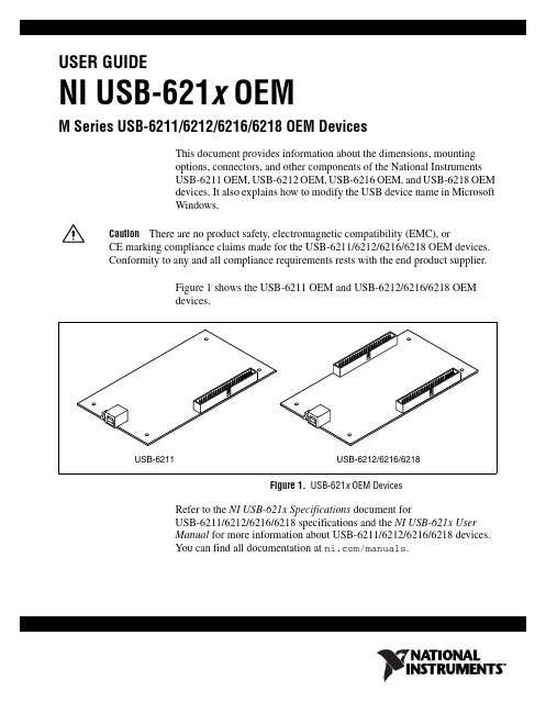
USER GUIDENI USB-621x OEMM Series USB-6211/6212/6216/6218 OEM DevicesThis document provides information about the dimensions, mounting options, connectors, and other components of the National Instruments USB-6211 OEM, USB-6212 OEM, USB-6216 OEM, and USB-6218 OEM devices. It also explains how to modify the USB device name in Microsoft Windows.CautionThere are no product safety, electromagnetic compatibility (EMC), orCE marking compliance claims made for the USB-6211/6212/6216/6218 OEM devices. Conformity to any and all compliance requirements rests with the end product supplier.Figure 1 shows the USB-6211 OEM and USB-6212/6216/6218 OEM devices.Figure 1. USB-621x OEM DevicesRefer to the NI USB-621x Specifications document forUSB-6211/6212/6216/6218 specifications and the NI USB-621x User Manual for more information about USB-6211/6212/6216/6218 devices. You can find all documentation at /manuals.DimensionsFigure2 shows the dimensions of the USB-6211 OEM device.Figure 2. USB-6211 OEM Dimensions in Inches (Millimeters)NI USB-621x OEM User Figure3 shows the dimensions of the USB-6212/6216/6218 OEM device.Figure 3. USB-6212/6216/6218 OEM Dimensions in Inches (Millimeters)© National Instruments Corporation3NI USB-621x OEM User GuideI/O Connector PinoutsRefer to the NI USB-621x User Manual at /manuals for moreinformation about USB-6211/6212/6216/6218 signals and how to connectthem.Figure4 shows the connector pinout on the USB-6211 OEM device.Figure 4. USB-6211 OEM Connector PinoutNI USB-621x OEM User USB-6216 OEM devices.Figure 5. USB-6212/6216 OEM Connector Pinout© National Instruments Corporation5NI USB-621x OEM User GuideNI USB-621x OEM User Guide Figure 6. USB-6218 OEM Connector PinoutNoteIn non-referenced single-ended (NRSE) mode, the USB-6218 OEM device measures AI <0..15> relative to the AI SENSE input, and AI <16..35> relative to AI SENSE 2.© National Instruments Corporation 7NI USB-621x OEM User GuideBoard Mounting the USB-621x OEMThe USB-621x OEM device can be mounted on a motherboard using the 50-pin connector(s) and board mount socket(s), as shown in Figures 7 and 8.NoteYou can use either one or both 50-pin connectors to board mount the USB-6212/6216/6218 OEM device.Figure 7. USB-621x OEM Mounting Using 50-Pin Connectors(USB-6218OEM Device Shown)Figure 8. USB-621x OEM Device Installed on Motherboard(USB-6218OEM Device Shown)Refer to the Device Components section for more information about mounting components.1Mo u nting S t a ndoff 2Bo a rd Mo u nt S ocket350-Pin Connector4US B-6218 OEM Device5Mo u nting ScrewsNI USB-621x OEM User Guide Device ComponentsTable 1 contains information about the components used for interfacing and interacting with the USB-621x OEM device.Modifying the USB Device Name in Microsoft WindowsYou can change how the USB-621x OEM device name appears when users install the device in both the Found New Hardware Wizard that appears when the device is initially installed and in the Windows Device Manager.Windows Vista/XP UsersFigure 9 depicts how a USB-6211 (OEM) device name appears in the Found New Hardware Wizard and Windows Device Manager.Table 1. USB-621x OEM ComponentsComponentReference Designator(s) on PCBManufacturer Manufacturer Part Number 50-pin connector J6*, J73M N2550-6002UB USB connectorJ5AMP 787780-150-pin board mount socket †—3M8550-4500PL (or equivalent)Mounting standoff,using board mount socket —RAF Electronic Hardware M1261-3005-SS ‡ with M3×0.5screw Mounting standoff, using ribbon cable—RAF Electronic Hardware2053-440-SS ** with 4-40 screw* J6 is available on USB-6212/6216/6218 OEM devices only.† You can use either one or both 50-pin connectors to board mount the USB-6212/6216/6218 OEM device.‡ 3/16 in. HEX female-to-female, 14 mm long.** 3/16 in. HEX female-to-female, 1/4 in. long.© National Instruments Corporation 9NI USB-621x OEM User GuideFigure 9. USB-6211 OEM Device in the Found New Hardware Wizardand Device Manager (Windows Vista/XP)To modify the device name in the Found New Hardware Wizard and Windows Device Manager in Microsoft Windows Vista/XP, complete the following steps.NoteYou must have NI-DAQmx 8.6 or later installed on your PC.1.Locate the OEM x .inf file in the y :\WINDOWS\inf\ directory, where x is the random number assigned to the INF file by Windows, and y :\is the root directory where Windows is installed.NoteNew security updates to Microsoft Vista and NI-DAQ 8.6 create random INF files for NI hardware. Windows assigns random file numbers to all INF files, which causes the user to search through several INF files until the correct file is located.If you want to revert back, save a copy of this file as OEM x _original.infin a different location.NI USB-621x OEM User Guide 2.Edit the device INF file by opening OEM x .inf with a text editor. At the bottom of this file are the descriptors where Windows looks to identify the device. Locate the two lines of text that contain in quotes the descriptors for the device name you are modifying. Change the descriptor on both lines to the new device name, as shown in Figure 10.Figure 10. INF File Descriptors Changed to “My Device” (Windows Vista/XP)3.Save and close the INF file.4.Go to the Windows Device Manager.(Windows Vista) In the Device Manager, notice that the OEM device now appears as My Device , as shown in Figure 11.(Windows XP) In the Device Manager, right-click the OEM device underData Acquisition Devices, and select Uninstall . Disconnect the USB cable from your PC.When you reconnect the device, it appears as My Device in the Found New Hardware Wizard and Windows Device Manager, as shown in Figure 11.NoteWhen the device is initially installed, the Windows alert message may display the following: Found New Hardware: M Series USB 621x (OEM). This message appears for a few seconds until the custom name appears and the Found New Hardware Wizard is launched. This alert message device name cannot be changed.Original FileModified File© National Instruments Corporation 11NI USB-621x OEM User GuideFigure 11. “My Device” in the Found New Hardware Wizard and Device Manager(Windows Vista/XP)Note Modifying the INF file will not change the USB-621x OEM device name inMeasurement & Automation Explorer (MAX).NI USB-621x OEM User Guide Windows 2000 UsersFigure 12 depicts how a USB-6211 (OEM) device name appears in theFound New Hardware Wizard and Windows Device Manager.Figure 12. USB-6211 OEM Device in the Found New Hardware Wizardand Device Manager (Windows 2000)To modify the device name in the Found New Hardware Wizard andWindows Device Manager in Windows 2000, complete the following steps.Note You must have NI-DAQmx 8.6 or later installed on your PC.1.Locate the nimioxsu.inf file in the x :\WINNT\inf\ directory,where x :\ is the root directory where Windows is installed.If you want to revert back, save a copy of this file asnimioxsu_original.infin a different location.© National Instruments Corporation 13NI USB-621x OEM User Guide2.Edit the device INF file by opening nimioxsu.inf with a text editor.At the bottom of this file are the descriptors where Windows looks toidentify the device. Locate the two lines of text that contain in quotesthe descriptors for the device name you are modifying. Change thedescriptor on both lines to the new device name, as shown in Figure 13.Figure 13. INF File Descriptors Changed to “My Device” (Windows 2000)3.Save and close the INF file.4.Go to the Windows Device Manager, right-click the OEM device under Data Acquisition Devices, and select Uninstall .5.Disconnect the USB cable from your PC.When you reconnect the device, it appears as My Device in the Found NewHardware Wizard and Windows Device Manager, as shown in Figure 14.NoteWhen the device is initially installed, the Windows alert message may display the following: Found New Hardware: M Series USB 621x (OEM). This message appears for a few seconds until the custom name appears and the Found New Hardware Wizard is launched. This alert message device name cannot be changed.Original FileModified FileNational Instruments, NI, , and LabVIEW are trademarks of National Instruments Corporation. Refer to the Terms of Use section on /legal for more information about NationalInstruments trademarks. Other product and company names mentioned herein are trademarks or trade names of their respective companies. For patents covering National Instruments products, refer to the appropriate location:Help»Patents in your software, the patents.txt file on your CD, or/patents .© 2006–2007 National Instruments Corporation. All rights reserved.372083C-01Oct07Figure 14. “My Device” in the Found New Hardware Wizardand Device Manager (Windows 2000)Note Modifying the INF file will not change the USB-621x OEM device name inMeasurement & Automation Explorer (MAX).。
NIUSB_datasheetNI数据采集卡手册
Industrial Digital I/O Device for USB –60 V, Channel-to-Channel IsolatedOverview and ApplicationsThe National Instruments USB-6525 is a full-speed USB device with eight normally open, channel-to-channel isolated, solid-state relay outputs and eight ±60 VDC channel-to-channel isolated digital inputs. The NI USB-6525 offers features for industrial control and manufacturing test applications, such as factory automation, embedded machine control, and production line verification. The solid-state relay outputs have a 60 VDC/30 V rms switching voltage and 500 mA/ch maximum switching current, making them ideal for controlling pumps, valves, motors, and other industrial actuators. The eight isolated digital input channels break ground loops and offer protection from noise and spikes on external signals. You can also use one of the digital input channels as a 5 kHz, 32-bit event counter for counting digital pulses.HardwareThe USB-6525 has eight channel-to-channel optically isolated inputs,P1.<0..7>, and eight channel-to-channel optically isolated, solid-state relay outputs, P0.<0..7>. The isolated inputs consist of an optocoupler, a depletion-mode MOSFET-based current-limiting circuit, and a Schottky diode. Each channel has its own positive and negative terminals capable of detecting a wide range of DC signals, from 5 V TTL logic levels to DC power supply levels up to 60 V.PFI 0 (an alias to P1.7) can also function as the source for a 32-bit counter. In this mode, the device counts low to high transitions on P1.7. You can arm and disarm the counter as well as read or reset the count through software.You can connect loads to the solid-state relay outputs with an AC or DC power source. The default power-on state of the solid-state relays is open. The relays also remain open when the computer and the USB-6525device are powered off.•Small, portable digital I/O device •Eight channel-to-channel optically isolated inputs (±60 VDC)•Eight channel-to-channel optically isolated, solid-state relay outputs (60 VDC/30 V rms max)•500 mA maximum switching current per channel•One 32-bit event counter•Full-speed USB (12 Mb/s) bus interface •Built-in, removable connectors for easy connectivity•USB cable strain relief Operating Systems•Windows Vista/XP/2000Recommended Software •LabVIEW•LabWindows™/CVI •Measurement Studio •LabVIEW SignalExpressOther Compatible Software •Visual Studio .NET•C, C++•Visual BasicMeasurement Services Software (included)•NI-DAQmx driver software •Measurement & Automation Explorer configuration utility•LabVIEW SignalExpress LEdata-logging softwareNI USB-6525IsolationIsolation is a form of built-in signal conditioning that provides an extended voltage range for direct connectivity to industrial sensors and actuators. The USB-6525 provides channel-to-channel isolation where each channel is physically and electrically separated from the others. Isolation provides three main benefits:1.Safety from hazardous high voltages and transients2.Rejection of common-mode voltages3.Removal of ground loopsSafety from High-Voltage TransientsIsolation electrically separates high-voltage front-end channels from each other and the low-voltage back end of the USB-6525. Signalsare passed between the two sections of the device using optocouplers. By separating the two sections, any voltages within the isolation specifications are prevented from entering the USB bus section or other channels. Isolation provides protection for the user, data acquisition system, and measurement data.Common-Mode Voltage RejectionA voltage common to both sides of a differential circuit pair iscalled common-mode voltage. This phenomenon is typical in noisy environments containing machinery and inductive loads. The differential voltage across the circuit pair is the desired signal, whereas the common voltage signal is the unwanted signal that may have been coupled into the transmission line. The USB-6525 can measure signals from lines with signal plus common-mode voltage of up to 60 VDC.Ground Loop RemovalGround loops are the most common source of noise in data acquisition applications. They occur when two connected terminals in a circuit are at different ground potentials, causing current to flow between thetwo points. This additional voltage can cause significant error in the measurement. When a ground loop exists, the measured voltage isthe sum of the signal voltage and the potential difference that exists between the signal source ground and the measurement system ground. This potential is generally not a DC level; therefore, the result is a noisy measurement system. By offering an isolated floating ground on the front end, the isolated USB-6525 devices are able to prevent ground loops from forming.SoftwareNational Instruments measurement services software, built aroundNI-DAQmx driver software, includes intuitive application programming interfaces, configuration tools, I/O assistants, and other tools designed to reduce system setup, configuration, and development time. National Instruments recommends using the latest version of NI-DAQmx driver software for application development in National Instruments LabVIEW, LabWindows/CVI, and Measurement Studio. To obtain the latest version of NI-DAQmx, visit /support/daq/versions. NI measurement services software speeds up your development with features including:•A guide to create fast and accurate measurements with no programming using DAQ Assistant•Automatic code generation to create your application in LabVIEW; LabWindows/CVI; LabVIEW SignalExpress; and Visual Studio .NET,C/C++/C#, or Visual Basic using Measurement Studio •Multithreaded streaming technology•More than 3,000 free software downloads to jump-start your project available at /zone•Software configuration of all digital I/O features without hardware switches/jumpers•Free LabVIEW SignalExpress LE data-logging softwareThe USB-6525 is compatible with the following versions (or later) of NI application software – LabVIEW, LabWindows/CVI, and Measurement Studio versions 7.x or LabVIEW SignalExpress. You can also use your NI digital I/O device with ANSI C, Microsoft Visual C++, Visual Basic, and the Microsoft .NET languages C# and Visual Basic .NET. The USB-6525 is not compatible with the Traditional NI-DAQ (Legacy) driver.Ordering InformationNI USB-6525..........................................................................779640-01 Includes NI-DAQmx software, LabVIEW SignalExpress LE data-logging software, anda USB cable.NI USB-6000 Series Prototyping Accessory........................779511-01 Includes breadboarding area with cover and strain relief.SpecificationsThese specifications are typical at 25 °C, unless otherwise noted.Isolated InputsNumber of channels............................8, ch-ch isolatedInput voltage range.............................-60 to 60 VDCDigital logic levelsInput current........................................ 3.0 mA/channel maxSolid-State Relay OutputsNumber of channels............................8, ch-ch isolatedRelay type...........................................Normally open solid-state relay(SSR)Switching voltage...............................60 VDC/30 V rms max Switching current (per channel).........500 mA max, full operationtemperature range Switching rate (90% duty cycle)......... 5 operations per second Relay open time..................................60 µs typRelay close time.................................. 1.2 ms typOn-resistance......................................550 mΩ, maxOff-leakage current (max)...................0.6 µA typCounterNumber of counters............................ 1 (P1.7 can be configured asa counter) Resolution...........................................32 bitsCounter measurements.......................rising edge counting Maximum input frequency.................. 5 kHzMinimum high pulse width.................20 µsMinimum low pulse width..................180 µsBus InterfaceUSB B 2.0 full-speed (12 Mb/s)Power RequirementsInput voltage....................................... 4.5 to 5.25 VDC in configuredstateActive current......................................150 mA maxSuspend current..................................350 µA typPhysical CharacteristicsDimensionsWithout connectors........................ 6.35 by 8.51 by 2.31 cm(2.50 by 3.35 by 0.91 in.)With connectors.............................8.18 by 8.51 by 2.31 cm(3.22 by 3.35 by 0.91 in.)I/O B series B receptacle,(2) 16 position (screw terminal)plug headers Screw-terminal wiring........................16 to 28 AWG copper conductorwire with 10 mm (0.39 in.) ofinsulation stripped from the end Torque for screw terminals.................0.22 to 0.25 N · m(2.0 to 2.2 lb in.)WeightWith connectors.............................Approx. 87 g (3.1 oz)Without connectors........................Approx. 64 g (2.3 oz)IsolationChannel-to-channel ............................60 VDC continuousChannel-to-earth ground ....................60 VDC continuous Withstand ..........................................60 VDC continuousNote:Do not use this module for connection to signals or for measurements within Measurement Categories II, III, or IV. EnvironmentNI 6528 and PXI-6529 devices are intended for indoor use only. Pollution degree (IEC-60664) (2)Operating EnvironmentAmbient temperature .........................0 to 55 °CRelative humidity................................10 to 90%, noncondensing Maximum altitude ..............................2,000 m at 25 °C ambienttemperature(tested in accordance with IEC-60068-2-1, IEC-60068-2-2, and IEC-60068-2-56)Storage EnvironmentAmbient temperature .........................-40 to 85 °CRelative humidity ...............................5% to 95%, noncondensing (tested in accordance with IEC-60068-2-1, IEC-60068-2-2, and IEC-60068-2-56)Safety and ComplianceSafetyThis product is designed to meet the requirements of the following standards of safety for electrical equipment for measurement, control, and laboratory use:•IEC 61010-1, EN 61010-1•UL 61010-1, CSA 61010-1Note:For UL and other safety certifications, refer to the product label or visit /certification, search by model number or product line, and click the appropriate link in the Certification column. Electromagnetic CompatibilityThis product is designed to meet the requirements of the following standards of EMC for electrical equipment for measurement, control, and laboratory use:•EN 61326 EMC requirements; Minimum Immunity•EN 55011 Emissions; Group 1, Class A•CE, C-Tick, ICES, and FCC Part 15 Emissions; Class ANote:For EMC compliance, operate this device according toproduct documentation.CE ComplianceThis product meets the essential requirements of applicable European Directives, as amended for CE marking, as follows:•73/23/EEC; Low-Voltage Directive (safety)•89/336/EEC; Electromagnetic Compatibility Directive (EMC) Note:Refer to the Declaration of Conformity (DoC) for this product for any additional regulatory compliance information. To obtain the DoC for this product, visit /certification, search by model number or product line, and click the appropriate link in the Certification column.Waste Electrical and Electronic Equipment (WEEE)EU Customers:At the end of their life cycle, all products must be sent to a WEEE recycling center. For more information about WEEE recycling centers and National Instruments WEEE initiatives, visit/environment/weee.htm.NI Services and SupportNI has the services and support to meet your needs around the globe and through the application life cycle – from planning and development through deployment and ongoing maintenance. We offer services and service levels to meet customer requirements in research,design, validation, and manufacturing. Visit /services .Training and CertificationNI training is the fastest, most certain route to productivity with our products. NI training can shorten your learning curve, save development time, and reduce maintenance costs over the application life cycle. We schedule instructor-led courses in cities worldwide, or we can hold a course at your facility. We also offer a professional certification program that identifies individuals who have high levels of skill and knowledge on using NI products. Visit /training .Professional ServicesOur NI Professional Services team is composed of NI applications and systems engineers and a worldwide National Instruments Alliance Partner program of more than 600 independent consultants andintegrators. Services range from start-up assistance to turnkey system integration. Visit /alliance .OEM SupportWe offer design-in consulting and product integration assistance if you want to use our products for OEM applications. For information about special pricing and services for OEM customers, visit /oem .Local Sales and Technical SupportIn offices worldwide, our staff is local to the country, giving you access to engineers who speak your language. NI delivers industry-leading technical support through online knowledge bases, our applications engineers, and access to 14,000 measurement and automationprofessionals within NI Developer Exchange forums. Find immediate answers to your questions at /support .We also offer service programs that provide automatic upgrades to your application development environment and higher levels of technical support. Visit /ssp .Hardware ServicesNI Factory Installation ServicesNI Factory Installation Services (FIS) is the fastest and easiest way to use your PXI or PXI/SCXI combination systems right out of the box.Trained NI technicians install the software and hardware and configure the system to your specifications. NI extends the standard warranty by one year on hardware components (controllers, chassis, modules)purchased with FIS. To use FIS, simply configure your system online with /pxiadvisor .Calibration ServicesNI recognizes the need to maintain properly calibrated devices for high-accuracy measurements. We provide manual calibration procedures, services to recalibrate your products, and automated calibration software specifically designed for use by metrology laboratories. Visit /calibration .Repair and Extended WarrantyNI provides complete repair services for our products. Express repair and advance replacement services are also available. We offerextended warranties to help you meet project life-cycle requirements. Visit /services.National Instruments • info@ • 800 813 3693*351494A-01*351494A-012007-8768-301-101-D。
- 1、下载文档前请自行甄别文档内容的完整性,平台不提供额外的编辑、内容补充、找答案等附加服务。
- 2、"仅部分预览"的文档,不可在线预览部分如存在完整性等问题,可反馈申请退款(可完整预览的文档不适用该条件!)。
- 3、如文档侵犯您的权益,请联系客服反馈,我们会尽快为您处理(人工客服工作时间:9:00-18:30)。
Technical SalesUnited States(866)531-6285info@! " #! "#$ %&'( $#) * + # ) # ," !! # !-+" -.( #" ) + # " * * "" #" ) ,"#/ 0 123,"# , "% ) " *4 $(25 4 5 6 %$( 3" #")" + #$ 7.2'.( 8&9): # ,"# + #" .(4 $(25 2: #" 42 "# ! ,"+ #"$ $ #'*".(/ 0 "#" " / 03 "# " ) + ! !; 8&9 ) " ) <" + # "# # !! # !- + ) # " 7( ++"# " !* " ) # " " * " " * " + # # # )) " # " = 7 = $ "#!* " # "# ! "# )"# 7> # ) # ," !! # !- +" - $ %&'( # , " 7'*"/ 0 " " "! + ! -+ #) " # !" ! # " ! 7? - ) ) <" ! + # " )" * " #"! !#" "#) ! "! , - "" ! ) + " ! "! 70"! " * ) " "#" +# )/ 0 - ! ! # "!" #-": "# "# " 7'*"/ 0 +" #" .( #" ) "!* - * !* ," - 83& " #"! * * "" #" ) + !# / 07> #) #" + #) .( #" ) , " *"@" #!" 7$ % #.( 8&9): # ,"# )" #")" "#, !" + #" # , " " - "! + # # # )) "#+ !" *+" #" !* *"8&9& *" #" !" "," )" )"73 "# " ", !" #" ! ) " * *"'# .( 8&9 4" !- # ,"#7&& ' ( % #2,"#-3 "# " 8&9 ", !" ! " ! - +.(4 $(25 2: #" 42 + #" - ! ; ! - !; #" -<" #" " * # # )) 7( 4 $(25 2: #" 3 "# " 8&9 ", !" #"! ) " * *"+ ,"# # "# +.( ! + #" 4 $(25A7 4 5 %$(A7: #3" #")" A7:73 "# " 8&9 ", !" #" ! ) " *$ 7.2' &. (% %BB $ 0 ! 7 7'*") # 4 5 " "# !" "+# )3 !# + % # # 75 #" "#" # ") # +3 !# + % # # *"/ " " *"#! # " 7& ' % ' (& ' % ' ( '!) ( 8" " "! + !8 *""& ' % ' ( !)) * & ' % ' ( !)) *" ' (-1# "#1 " # -> :7. , " " "! L1# "# -? # . ) "#L + "# *"L0 " %" "#L "! 771 !"- * ," " - # ") - #! # "" *"LC #% #1 L "! !"- # # "# ; " # # + :+ #)71# "# -?* "% !"- # # "# # ; "7% #+ &2 ' " - )) (-AA A.(4 $(25> 8"," )" - ")+ #5 2 * .(@"! ))" " H DDAA A 4 $(25& ! 0 "#+ #5 2 *.(@"! ))" "H DDDAA F .(4 $(25@" # M" "# ' + #3 !# + 1++ !"H DAA A8(& ")& , !" 2 2 *H DD. 4 " - )) (-AA4 5 %$(> 8"," )" - ")+ #5H DDAA .(3" #")" ?# +" 2 + #3 !# +$H FDAA A8(& ")& , !" 2 2 *H DDOther compatible software:ANSI C/C++,C#,Visual Basic .NETK C * ," " "! " *"/ " " *"! #- *"#"- " *" # ! 7?# ! ) -* ,"!* " !"- # " * ! )" D 7? " ", ""! ##" # ! 7$ % #$ " 8# ,"# / " " #!*& 8# ,"#" ' 6 ( ! 1# "#1 " # -> :7. , " " "! L1# "# -? # . ) "#L + "# *"L0 " %" "#L "! 771 !"- * ," " - # ") - #! # "" *"LC #% # 1 L "! !"- # # "# ; " # # + :+ #)71# "# -?* "% !"- # # "# # ; "7$ '34 ( 9 (. ( # )" " ) + ! #" # ! ) ) <"+ #" * ","# ": "! " + #" ! !! #72: " " ## " # , " + :" "! ) ! # !" *" )" + - ") #!* " ! ,"# -#" #! + # *#""-" # 7( *"- ++"# *"+ " "+ N+ ! ! , ! ) #" , #" # ! "> ! ! #" # -.( - )" *" - ") # ! +& # #! ! ,"#" " - O )" "" " #" #" *"* # #" ) + ! # "! + !> #) #" + #) - # ## - N4" # 3 #"& 5 ## - "#, !" P* N 7 7! ) "#, !" ## -7* )Q' 2: "# & 2: " " 5 ## " PO , !# N " % 3"5 %'& ! )" 7#"+"##"# R S/ S Q $ " 5 ## -@" #? ! " P* N 7 7! ) "#, !" ## -T#" #T ! " 7* )Q1 6 (.(#"! <" *" "" ) # "# -! # " ", !" + #* * !! # !-)" #")" 7.(# , " ) ! # # !" #" "#, !" #"! # "- # # ! ) " ! # + #" ! # ") -.()" #")" # ! 74" # 3 #"& % # "#, !" P* N 7 7! ) "#, !" ! # 7* )Q. ( (-.( # *"+ " ) !"# # " # ! , - *.( !!" + ! "," )" 74" # 3 #"& .('# %"# + ! P* N 7 7! ) # Q> % # "." #C $ " !*" " P* N "7 7! ) + ,7! " Q/ & $ '@" # - ##" "#" # ! "# ## - # # ! 7.( ++"# + ! ! #" # - )" *" - ")+ " - O )" "" " #" #" *"* # #" ) + ! # "! + ! 74" # 3 #"& @" # "#, !" P* N 7 7! ) "#, !" ## -7* )Q% ! .( @" # 3 "# & * # < @3& + #) * # ! 7P* N "7 7! ) + !!7! T)"Q$ " - #@3& # #"; " "7P* N 7 7! ) # "#, !"#"; Q@" "#- # # ! P* N 7 7! ) #" "#Q7. '2( ' !&&7! ) # P* N 7 7! ) # Q/ ! '( " !' (% ) (3 D8 )" 8#?# ! %"# + !/ (% ) (.(/ 08 &!; + #1238 .(8 &!; 8# ,"#.(4 $(25 2: #" ( "# ! ,"8 4 + #".( #" ) N0 #"! G * "" 8 #" ) ,"#/ 0U . ( # )" % # # 7& # * #" "#," 7。