ID82C86HZ中文资料
ID82C52资料

March 199782C52 CMOS Serial Controller InterfaceFeatures•Single Chip UART/BRG•DC to 16MHz (1M Baud) Operation•Crystal or External Clock Input•On-Chip Baud Rate Generator - 72 Selectable Baud Rates•Interrupt Mode with Mask Capability •Microprocessor Bus Oriented Interface•80C86 Compatible•Single +5V Power Supply•Low Power Operation . . . . . . . . . . . . . . .1mA/MHz Typ •Modem Interface•Line Break Generation and Detection•Operating Temperature Range:-C82C52 . . . . . . . . . . . . . . . . . . . . . . . . . .0o C to +70o C -I82C52 . . . . . . . . . . . . . . . . . . . . . . . . .-40o C to +85o C -M82C52 . . . . . . . . . . . . . . . . . . . . . . .-55o C to +125o C DescriptionThe Intersil 82C52 is a high performance programmable Universal Asynchronous Receiver/Transmitter (UART) and Baud Rate Generator (BRG) on a single chip. Utilizing the Intersil advanced Scaled SAJI IV CMOS process, the 82C52 will support data rates up to 1M baud asynchronously with a 16X clock (16MHz clock frequency).The on-chip Baud Rate Generator can be programmed for any one of 72 different baud rates using a single industry standard crystal or external frequency source. A unique pre-scale divide circuit has been designed to provide standard RS-232-C baud rates when using any one of three industry standard crystals (1.8432MHz, 2.4576MHz, or 3.072MHz).A programmable buffered clock output (CO) is available and can be programmed to provide either a buffered oscillator or 16X baud rate clock for general purpose system usage.PinoutsOrdering InformationPACKAGETEMPERATURERANGE1M BAUD PKG. NO.PDIP0o C to +70o C CP82C52E28.6-40o C to +85o C IP82C52E28.6PLCC0o C to +70o C CS82C52N28.45-40o C to +85o C IS82C52N28.45CERDIP0o C to +70o C CD82C52F28.6-40o C to +85o C ID82C52F28.6-55o C to +125o C MD82C52/B F28.6SMD#8501501XA F28.6CLCC-55o C to +125o C MR82C52/B J28.ASMD#85015013A J28.A82C52 (PDIP, CERDIP)TOP VIEW82C52 (PLCC, CLCC)TOP VIEW2827262524232221201918171615RDWRD0D1D2D3D4D5D6D7A0A1IXOX1234567891011121314CSODRSDIINTRRSTCODTRDSRCTSGNDSDOVCCTBRERTS23242522212019113214141516171812132827261056789D2D3D4D5D6D7A0SDIINTRRSTTBRECORTSDTRA1IXOXSDOGNDDSRCTSD1DWRRDCSODRVCCFile Number2950.1CAUTION: These devices are sensitive to electrostatic discharge; follow proper IC Handling Procedures.Block DiagramPin DescriptionSYMBOL PIN NO.TYPE ACTIVE LEVEL DESCRIPTIONRD1ILowREAD:The RD input causes the 82C52 to output data to the data bus (D0-D7). The data output depends upon the state of the address inputs (A0-A1).CS0 enables the RD input.WR 2I LowWRITE:The WR input causes data from the data bus (D0-D7) to be input to the 82C52.Addressing and chip select action is the same as for read operations.D0-D73-10I/O HighDA TA BITS 0-7:The Data Bus provides eight, three-state input/output lines for the transfer of data, control and status information between the 82C52 and the CPU. For character formats of less than 8 bits, the corresponding D7, D6 and D5 are considered “don't cares” for data WRITE operations and are 0 for data READ operations. These lines are normally in a high impedance state except during read operations. D0 is the Least Significant Bit (LSB) and is the first serial data bit to be received or transmitted.A0, A111, 12I HighADDRESS INPUTS:The address lines select the various internal registers during CPU bus operations.IX, OX 13, 14I/OCRYSTAL/CLOCK:Crystal connections for the internal Baud Rate Generator. IX can also be used as an external clock input in which case OX should be left open.SDO 15OHighSERIAL DA TA OUTPUT:Serial data output from the 82C52 transmitter circuitry. A Mark (1) is a logic one (high) and Space (0) is logic zero (low). SD0 is held in the Mark condition when CTS is false, when RST is true, when the Transmitter Register is empty, or when in the Loop Mode.GND 16Low GROUND:Power supply ground connection.CTS17ILowCLEAR TO SEND:The logical state of the CTS line is reflected in the CTS bit of the Modem Status Register. Any change of state in CTS causes INTR to be set true when INTEN and MIEN are true. A false level on CTS will inhibit transmission of data on the SD0 output and will hold SD0 in the Mark (high) state. If CTS goes false during transmission, the current character being transmitted will be completed.CTS does not affect Loop Mode operation.READ/WRITE CONTROL LOGICDATA BUS BUFFERPROGRAM-MABLEBOUD RATE CONTROLLOGIC3 - 10121112RD WR A0A128CSO 1421OX CO2324RST INTR13IX GENERATORI N T E R N A L D A T A B U STRANSMITTERBUFFER REGISTER UARTCONTROL ANDSTATUS RECEIVER BUFFER REGISTER MODEM CONTROL ANDREGISTERSSTATUS REGISTERS18DSR 17CTS 19DTR 20RTSTRANSMITTER REGISTER P RECEIVER REGISTER P S1525SDOSDI2226TBRE DRSD0-D7DSR18ILowDA TA SET READY:The logical state of the DSR line is reflected in the Modem Status Register.Any change of state of DSR will cause INTR to be set if INTEN and MIEN are true. The state of this signal does not affect any other circuitry within the 82C52.DTR 19O LowDA TA TERMINAL READY:The DTR signal can be set (low) by writing a logic 1 to the appro-priate bit in the Modem Control Register (MCR). This signal is cleared (high) by writing a logic 0 in the DTR bit in the MCR or whenever a reset (RST = high) is applied to the 82C52.RTS 20O LowREQUEST TO SEND:The RTS signal can be set (low) by writing a logic 1 to the appropriate bit in the MCR. This signal is cleared (high) by writing a logic 0 to the RTS bit in the MCR or whenever a reset (RST = high) is applied to the 82C52.CO 21OCLOCK OUT:This output is user programmable to provide either a buffered IX output or a buffered Baud Rate Generator (16X) clock output. The buffered IX (Crystal or external clock source) output is provided when the Baud Rate Select Register (BRSR) bit 7 is set to a zero.Writing a logic one to BRSR bit 7 causes the CO output to provide a buffered version of the internal Baud Rate Generator clock which operates at sixteen times the programmed baud rate. On reset D7 (CO select) is reset to 0.TBRE 22OHighTRANSMITTER BUFFER REGISTER EMPTY:The TBRE output is set (high) whenever the T ransmitter Buffer Register (TBR) has transferred its data to the T ransmit Register. Application of a reset (RST) to the 82C52 will also set the TBRE output. TBRE is cleared (low) whenever data is written to the TBR.RST 23I HighRESET:The RST input forces the 82C52 into an “Idle” mode in which all serial data activities are suspended. The Modem Control Register (MCR) along with its associated outputs are cleared. The UART Status Register (USR) is cleared except for the TBRE and TC bits, which are set. The 82C52 remains in an “Idle” state until programmed to resume serial data activities.The RST input is a Schmitt triggered input.INTR 24O HighINTERRUPT REQUEST:The INTR output is enabled by the INTEN bit in the Modem Control Register (MCR). The MIEN bit selectively enables modem status changes to provide an input to the INTR logic. Figure 9 in Design Information shows the overall relationship of these inter-rupt control signals.SDI 25I HighSERIAL DA TA INPUT:Serial data input to the 82C52 receiver circuits. A Mark (1) is high, and a Space (0) is low. Data inputs on SDI are disabled when operating in the loop mode or when RST is true.DR 26O HighDA TA READY:A true level indicates that a character has been received, transferred to the RBR, and is ready for transfer to the CPU. DR is reset on a data READ of the Receiver Buffer Register (RBR) or when RST is true.V CC 27HighV CC :+5V positive power supply pin. A 0.1µF decoupling capacitor from V CC (Pin 27) to GND (Pin 16) is recommended.CS028I LowCHIP SELECT:The chip select input acts as an enable signal for the RD and WR input signals.Pin Description (Continued)SYMBOL PIN NO.TYPE ACTIVE LEVEL DESCRIPTIONResetDuring and after power-up, the 82C52 Reset Input (RST) must be held high for at least two IX clock cycles in order to initialize and drive the 82C52 circuits to an idle mode until proper programming can be done. A high on RST causes the following events to occur•Resets the internal Baud Rate Generator (BRG) circuit clock counters and bit counters. The Baud Rate Select Register (BRSR) is not affected (except for bit 7 which is reset to 0).•Clears the UART Status Register (USR) except for T ransmission Complete (TC) and T ransmit Buffer Register Empty (TBRE) which are set. The Modem Control Register (MCR) is also cleared. All of the discrete lines, memory elements and miscellaneous logic associated with these register bits are also cleared or turned off. Note that the UART Control Register (UCR) is not affected. Following removal of the reset condition (RST = low), the 82C52 remains in the idle mode until programmed to its desired system configuration.Programming The 82C52The complete functional definition of the 82C52 is programmed by the systems software. A set of control words (UCR, BRSR and MCR) must be sent out by the CPU to initialize the 82C52 to support the desired communication format. These control words will program the character length, number of stop bits, even/odd/no parity, baud rate, etc. Once programmed, the 82C52 is ready to perform its communication functions.The control registers can be written to in any order. However, the MCR should be written to last because it controls the interrupt enables, modem control outputs and the receiver enable bit. Once the 82C52 is programmed and operational, these registers can be updated any time the 82C52 is not immediately transmitting or receiving data.T able 1. Shows the control signals required to access 82C52 internal registers.UART Control Register (UCR)The UCR is a write only register which configures the UART transmitter and receiver circuits. Data bits D7 and D6 are not used but should always be set to a logic zero (0) in order to insure software compatibility with future product upgrades. During the Echo Mode, the transmitter always repeats the received word and parity, even when the UCR is programmed with different or no parity. See Figure 1.TABLE 1.CS0A1A0WR RD OPERATION00001Data Bus→ Transmitter BufferRegister (TBR)00010Receiver Buffer Register(RBR)→ Data Bus00101Data Bus→ UART ControlRegister (UCR)00110UART Status Register(USR)→ Data Bus01001Data Bus→ Modem ControlRegister (MCR)01010MCR→ Data Bus01101Data Bus→ Bit Rate SelectRegister (BRSR)01110Modem Status Register(MSR)→ Data BusD7D6D5D4D3D2D1D0Stop BitSelect0 = 1 Stop Bits1 = 1.5 Stop Bits (Tx)and 1 Stop Bit (Rx)If 5 Data Bits Selected1 =2 Stop Bits for 6, 7or 8 Data Bits SelectedParityControl000 = Tx and Rx Even001 = Tx and Rx Odd010 = Tx Even, RxOdd011 = Tx Odd, RxEven100 = Tx Even, RxCheck Disabled101 = Tx Odd, RxCheck Disabled11X = Generation andCheck DisabledWordLengthSelect00 = 5 Bits01 = 6 Bits10 = 7 Bits11 = 8 BitsReserved Set to 00 for FutureProduct UpgradeCompatibilityFIGURE 1.UCRBaud Rate Select Register (BRSR)The 82C52 is designed to operate with a single crystal or external clock driving the IX input pin. The Baud Rate Select Register is used to select the divide ratio (one of 72) for the internal Baud Rate Generator circuitry. The internal circuitry is separated into two separate counters, a Prescaler and a Divisor Select. The Prescaler can be set to any one of four division rates,÷1,÷3,÷4, or÷5.The Prescaler design has been optimized to provide standard baud rates using any one of three popular crystal frequencies. By using one of these common system clock frequencies, 1.8432MHz, 2.4576MHz or 3.072MHz and Prescaler divide ratios of÷3,÷4, or÷5 respectively, the Prescaler output will provide a constant 614.4KHz. When this frequency is further divided by the Divisor Select counter, any of the standard baud rates from 50 Baud to 38.4Kbaud can be selected (see T able 2). Non-standard baud rates up to 1Mbaud can be selected by using different input frequencies (crystal or an external frequency input up to 16MHz) and/or different Prescaler and Divisor Select ratios.Regardless of the baud rate, the baud rate generator provides a clock which is 16 times the desired baud rate. For example, in order to operate at a 1Mbaud data rate, a16MHz crystal, a Prescale rate of÷1, and a Divisor Select rate of “external” would be used. This would provide a 16MHz clock as the output of the Baud Rate Generator to the T ransmitter and Receiver circuits.The CO select bit in the BRSR selects whether a buffered version of the external frequency input (IX input) or the Baud Rate Generator output (16x baud rate clock) will be output on the CO output (pin 21). The Baud Rate Generator output will always be a 50% nominal duty cycle except when “exter-nal” is selected and the Prescaler is set to÷3 or÷5.NOTE:These baud rates are based upon the following input frequency/ Prescale divisor combinations.1.8432MHz and Prescale =÷ 32.4576MHz and Prescale =÷ 43.072MHZ and Prescale =÷ 5†All baud rates are exact except for:Modem Control RegisterThe MCR is a general purpose control register which can be written to and read from. The RTS and DTR outputs are directly controlled by their associated bits in this register. Note that a logic one asserts a true logic level (low) at these output pins. The Interrupt Enable (INTEN) bit is the overall control for the INTR output pin. When INTEN is false, INTR is held false (low).The Operating Mode bits configure the 82C52 into one of four possible modes. “Normal” configures the 82C52 for nor-mal full or half duplex communications. “T ransmit Break”' enables the transmitter to only transmit break characters (Start, Data and Stop bits all are logic zero). The Echo Mode causes any data that is received on the SDI input pin to be retransmitted on the SDO output pin. Note that this output is a buffered version of the data seen on the SDI input and is not a resynchronized output. Also note that normal UART transmission via the T ransmitter Register is disabled when operating in the Echo mode (see Figure 4). The Loop T est Mode internally routes transmitted data to the receiver circuitry for the purpose of self test. The transmit data isD7D6D5D4D3D2D1D0Prescaler Select 00 =÷ 101 =÷ 310 =÷ 411 =÷ 5Divisor Select 00000 =÷ 200001 =÷ 400010 =÷ 16/3 00011 =÷ 800100 =÷ 32/3 00101 =÷ 1600110 =÷ 58/3 00111 =÷ 2201000 =÷ 3201001 = ÷ 6401010 =÷ 128 01011 =÷ 192 01100 =÷ 256 01101 =÷ 288 01110 =÷ 352 01111 =÷ 512 10000 =÷ 768 11111 = External (÷ 1)CO Select 0 = IX Output1 = Brg Output (On Reset, D7 (CO Select) is Reset to 0)FIGURE 2.BRSRTABLE 2.BAUD RATE DIVISOR38.4K External19.2K296004720016/348008360032/32400162000†58/31800†2212003260064300128200192150256134.5†288110†3527551250768BAUD RATE ACTUAL PERCENT ERROR 18001745.45 3.03%20001986.20.69%134.5133.330.87%110109.090.83%disabled from the SDO output pin. The Receiver Enable bit gates off the input to the receiver circuitry when in the false state.Modem Interrupt Enable will permit any change in modem status line inputs (CTS,DSR) to cause an interrupt when this bit is enabled. Bit D7 must always be written to with a logic zero to insure correct 82C52 operation.UART Status Register (USR)The USR provides a single register that the controlling sys tem can examine to determine if errors have occurred or if other status changes in the 82C52 require attention. For this reason, the USR is usually the first register read by the CPU to determine the cause of an interrupt or to poll the status of the 82C52.Three error flags OE, FE and PE report the status of any error conditions detected in the receiver circuitry. These error flags are updated with every character received during reception of the stop bits. The Overrun Error (OE) indicates that a character in the Receiver Register has been received and cannot be transferred to the Receiver Buffer Register (RBR) because the RBR was not read by the CPU. Framing Error (FE) indicates that the last character received in the RBR contained improper stop bits. This could be caused by the absence of the required stop bit(s) or by a stop bit(s) that was too short to be properly detected. Parity Error (PE) indi-cates that the last character received in the RBR contained a parity error based on the programmed parity of the receiver and the calculated parity of the received character data and parity bits.The Received Break (RBRK) status bit indicates that the last character received was a break character. A break character would be considered to be an invalid data character in that the entire character including parity and stop bits are a logic zero.The Modem Status bit is set whenever a transition is detected on any of the Modem input lines (CTS or DSR). A subsequent read of the Modem Status Register will show the state of these two signals. Assertion of this bit will cause an interrupt (INTR) to be generated if the MIEN and INTEN bits in the MCR register are enabled.The Transmission Complete (TC) bit indicates that both the TBR and Transmitter Registers are empty and the 82C52has completed transmission of the last character it was com-manded to transmit. The assertion of this bit will cause an interrupt (INTR) if the INTEN bit in the MCR register is true.The T ransmitter Buffer Register Empty (TBRE) bit indicates that the TBR register is empty and ready to receive another character.The Data Ready (DR) bit indicates that the RBR has been loaded with a received character (including Break) and that the CPU may access this data.Assertion of the TBRE or DR bits do not affect the INTR logic and associated INTR output pin since the 82C52 has been designed to provide separate requests via the DR and TBRE output pins. If a single interrupt for any status change in the 82C52 is desired this can be accomplished by using an 82C59A Interrupt controller with DR, TBRE, and INTR as inputs. (See Figure 11).D7D6D5D4D3D2D1D0Request to Send (RTS)0 =RTS Output High †1 =RTS Output Low Data Terminal Ready (DTR)0 =DTR Output High 1 =DTR Output Low Interrupt Enable (INTEN) 1 = Interrupts Enabled 0 = interrupts Disabled Mode Select00 = Normal01 = T ransmit Break 10 = Echo Mode11 = Loop T est ModeReceiver Enable (REN)0 = Not Enabled 1 = Enabled Modem Interrupt Enable (MIEN)0 = Not Enabled 1 = Enabled Must be Set to a Logic 0 for Normal 82C52 Operation†See Modem Status Register description for a description of register flag images with respect to output pins.FIGURE 3.MCRFIGURE 4.LOOP AND ECHO MODE FUNCTIONALITYSERIAL DATAFROMTRANSMITTERREGISTER ECHO MODESERIAL DATA TO RECEIVERREGISTERSDO PIN 15SDI PIN 25LOOP MODEModem Status Register (MSR)The MSR allows the CPU to read the modem signal inputs by accessing the data bus interface of the 82C52. Like all of the register images of external pins in the 82C52, true logic levels are represented by a high (1) signal level. By following this consistent definition, the system software need not be concerned with whether external signals are high or low true. In particular, the modem signal inputs are low true, thus a 0 (true assertion) at a modem input pin is represented by a 1 (true) in the MSR.Any change of state in any modem input signals will set the Modem Status (MS) bit in the USR register. When this hap-pens, an interrupt (INTR) will be generated if the MIEN and INTEN bits of the MCR are enabled.The Data Set Ready (DSR) input is a status indicator from the modem to the 82C52 which indicates that the modem is ready to provide received data to the 82C52 receiver cir-cuitry.Clear to Send (CTS) is both a status and control signal from the modem that tells the 82C52 that the modem is ready to receive transmit data from the 82C52 transmitter output (SDO). A high (false) level on this input will inhibit the 82C52 from beginning transmission and if asserted in the middle of a transmission will only permit the 82C52 to finish transmis-sion of the current character.Receiver Buffer Register (RBR)The receiver circuitry in the 82C52 is programmable for 5, 6, 7 or 8 data bits per character. For words of less than 8 bits, the data is right justified to the Least Significant Bit (LSB = D0). Bit D0 of a data word is always the first data bit received. The unused bits in a less than 8-bit word, at the parallel interface, are set to a logic zero (0) by the 82C52. Received data at the SDI input pin is shifted into the Receiver Register by an internal 1x clock which has been synchronized to the incoming data based on the position of the start bit. When a complete character has been shifted into the Receiver Register, the assembled data bits are par-allel loaded into the Receiver Buffer Register. Both the DR output pin and DR flag in the USR register are set. This dou-ble buffering of the received data permits continuous recep-tion of data without losing any of the received data.While the Receiver Register is shifting a new character into the 82C52, the Receiver Buffer Register is holding a previ-ously received character for the system CPU to read. Failure to read the data in the RBR before complete reception of the next character can result in the loss of the data in the Receiver Register. The OE flag in the USR register indicates the overrun condition.Transmitter Buffer Register (TBR)The Transmitter Buffer Register (TBR) accepts parallel data from the data bus (D0-D7) and holds it until the T ransmitter Register is empty and ready to accept a new character for transmission. The transmitter always has the same word length and number of stop bits as the receiver. For words of less than 8 bits the unused bits at the microprocessor data bus are ignored by the transmitter.D7D6D5D4D3D2D1D0Parity Error (PE)0 = No Error1 = ErrorFraming Error (FE)0 = No Error1 = ErrorOverrun Error (OE)0 = No Error1 = ErrorReceived Break (RBRK)0 = No Break1 = BreakModem Status (MS)0 = No StatusChange 1 = StatusChangeT ransmission Complete (TC)0 = NotComplete 1 = CompleteT ransmitter Buffer Register Empty (TBRE)0 = Not Empty1 = EmptyData Ready (DR)0 = Not Ready1 = ReadyFIGURE R D7D6D5D4D3D2D1D0Clear to Send (CTS)0 = False1 = TruerData Set Ready (DSR)0 = False1 = TrueUndefined FIGURE 6.MSR D7D6D5D4D3D2D1D0Bit 0Bit 1Bit 2Bit 3Bit 4Bit 5Bit 6Bit 7FIGURE 7.RBRD7D6D5D4D3D2D1D0Bit 0Bit 1Bit 2Bit 3Bit 4Bit 5Bit 6Bit 7FIGURE 8.TBR5-BitWord6-BitWord7-BitWord8-BitWord5-BitWord6-BitWord7-BitWord8-BitWordBit 0, which corresponds to D0 at the data bus, is always the first serial data bit transmitted. Provision is made for the transmitter parity to be the same or different from the receiver. The TBRE output pin and flag (USR register) reflect the status of the TBR. The TC flag (USR register) indicates when both TBR and TR are empty.82C52 Interrupt StructureThe 82C52 has provisions for software masking of interrupts generated for the INTR output pin. Two control bits in the MCR register, MIEN and INTEN, control modem status inter-rupts and overall 82C52 interrupts respectively. Figure 9illustrates the logical control function provided by these sig-nals.The modem status inputs (DSR and CTS) will trigger the edge detection circuitry with any change of status. Reading the MSR register will clear the detect circuit but has no effect on the status bits themselves. These status bits always reflect the state of the input pins regardless of the mask con-trol signals. Note that the state (high or low) of the status bits are inverted versions of the actual input pins.The edge detection circuits for the USR register signals will trigger only for a positive edge (true assertion) of these sta-tus bits. Reading the USR register not only clears the edge detect circuit but also clears (sets to 0) all of the status bits.The output pins associated with these status bits are not affected by reading the USR register.A hardware reset of the 82C52 sets the TC status bit in the USR. When interrupts are subsequently enabled an interrupt can occur due to the fact that the positive edge detection cir-cuitry in the interrupt logic has detected the setting of the TC bit. If this interrupt is not desired the USR should be read prior to enabling interrupts.This action resets the positive edge detection circuitry in the interrupt control logic (Figure 9).NOTE:For USR and MSR, the setting of status bits is inhibited during status register READ operations. If a status condition is gen-erated during a READ operation, the status bit is not set until the trail-ing edge of the RD pulse.If the bit was already set at the time of the READ operation, and the same status condition occurs, that status bit will be cleared at the trailing edge of the RD pulse instead of being set again.Software ResetA software reset of the 82C52 is a useful method for returning to a completely known state without exercising a complete system reset. Such a reset would consist of writing to the UCR, BRSR and MCR registers. The USR and RBRregisters should be read prior to enabling interrupts in order to clear out any residual data or status bits which may be invalid for subsequent operation.Crystal OperationThe 82C52 crystal oscillator circuitry is designed to operate with a fundamental mode, parallel resonant crystal. This cir-cuit is the same one used in the Intersil 82C84A clock gener-ator/driver. To summarize, Table 3 and Figure 10 show the required crystal parameters and crystal circuit configuration respectively.When using an external clock source, the IX input is driven and the OX output is left open. Power consumption when using an external clock is typically 50% of that required when using a crystal. This is due to the sinusoidal nature of the drive circuitry when using a crystal.82C52 - 80C86 InterfacingThe following example (Figure 11) shows the interface for an 82C52 in an 80C86 system.Use of the Intersil CMOS Interrupt Controller (82C59A) is optional and necessary only if an interrupt driven system is desired.By using the Intersil CMOS 82C84A clock generator, the system can be built with a single crystal providing both the processor clock and the clock for the 82C52. The 82C52 has special divider circuitry which is designed to supply industry standard baud rates with a 2.4576MHz input ing a 15MHz crystal as shown, results in less than a 2%frequency error which is adequate for many applications. For more precise baud rate requirements, a 14.7456MHz crystal will drive the 80C86 at 4.9MHz and provide the 82C52 with the standard baud rate input frequency of 2.4576MHz. If baud rates above 156Kbaud are desired, the OSC output can be used instead of the PCLK (÷6) output for asynchro-nous baud rates up to 1Mbaud.FIGURE 9.82C52 INTERRUPT STRUCTURERD (MSR)RBRK, TC OE, FE, PE(USR)RD (USR)DSR,CTS(MSR)INTR PIN 24INTEN (MCR)MIEN (MCR)POS.EDGE DETECTPOS. OR NEG.EDGE DETECTTABLE 3.PARAMETER TYPICAL CRYSTAL SPECIFICATIONFrequency 1.0 to 16MHzType of Operation Parallel Resonant, Fundamental Mode Load Capacitance (CL)20 or 32pF (Typ)R SERIES (Max)100Ω (f = 16MHz, CL = 32pF)200Ω (f = 16MHz, CL = 20pF)NOTE:C1 = C2 = 20pF For CL = 20pFC1 = C2 = 47pF For CL = 32pFFIGURE 10.C1 (NOTE)GNDC2 (NOTE)IX OX82C52。
三星8262d是什么cpu

三星8262d是什么cpu网友们知道什么是三星8262D的CPU吗?下面是店铺带来的关于三星8262d是什么cpu的内容,欢迎阅读!三星8262d是什么cpu:三星I8262D采用的是:1.CPU(处理器):1.2GHz 双核。
2.内存:总ROM内存为4GB,可用空间约为1.33GB;总RAM约768MB;外置存储卡:最大支持32GB micro SD卡。
3.摄像头:采用500万像素的后置摄像头,不支持前置摄像头。
支持闪光灯;支持自动对焦;支持4倍变焦(音量键)。
4.软件格式:APK5.蓝牙版本:蓝牙3.0三星是韩国的知名公司之一,是韩国最大的企业集团三星集团的简称,该集团包括44个下属公司及若干其他法人机构,成长为“世界最受尊敬企业”企业之一的三星在全世界68个国家拥有429个据点23万员工,业务涉及电子、金融、机械、化学等众多领域。
三星集团成立于1938年,公司最初主要出口朝鲜南半岛的鱼干、蔬菜和水果,逐步扩展为制糖、制药、纺织等制造业,并确立为家族制企业。
旗下子公司包含:三星电子、三星SDI、三星SDS、三星电机、三星康宁、三星网络、三星火灾、三星证券、三星物产、三星重工、三星工程、三星航空和三星生命等,由家族内的李氏成员管理,其中三间子公司被美国《财富》杂志评选为世界500强企业。
三星电子是旗下最大的子公司,是全球第二大手机生产商、全球营收最大的电子企业,2009年全球500强企业中,三星电子占据了第40位的一席之地。
全球最受尊敬企业排名第50位,三星的品牌价值排名第19位,较2008年又有了2位的进步。
在2011年的全球企业市值中为1500亿美元。
相关阅读推荐:1938年3月1日,三星前任会长李秉喆以30000韩元在韩国李秉喆大邱市成立了“三星商会”。
李秉喆早期的主要业务是将韩国的干鱼、蔬菜、水果等出口到中国的北京及满洲里。
1950年代逐步扩展为制糖、制药、纺织等制造业,并确立为家族制企业。
IP82C54中文资料

March 199782C54 CMOS Programmable Interval TimerFeatures•8MHz to 12MHz Clock Input Frequency•Compatible with NMOS 8254-Enhanced Version of NMOS 8253•Three Independent 16-Bit Counters•Six Programmable Counter Modes•Status Read Back Command•Binary or BCD Counting•Fully TTL Compatible•Single 5V Power Supply•Low Power-ICCSB . . . . . . . . . . . . . . . . . . . . . . . . . . . . . . . . . .10µA -ICCOP . . . . . . . . . . . . . . . . . . . . . . . . . .10mA at 8MHz •Operating Temperature Ranges-C82C54 . . . . . . . . . . . . . . . . . . . . . . . . . .0o C to +70o C -I82C54 . . . . . . . . . . . . . . . . . . . . . . . . .-40o C to +85o C -M82C54 . . . . . . . . . . . . . . . . . . . . . . .-55o C to +125o C DescriptionThe Intersil 82C54 is a high performance CMOS Program-mable Interval Timer manufactured using an advanced 2 micron CMOS process.The 82C54 has three independently programmable and functional 16-bit counters, each capable of handling clock input frequencies of up to 8MHz (82C54) or 10MHz (82C54-10) or 12MHz (82C54-12).The high speed and industry standard configuration of the 82C54 make it compatible with the Intersil 80C86, 80C88, and 80C286 CMOS microprocessors along with many other industry standard processors. Six programmable timer modes allow the 82C54 to be used as an event counter, elapsed time indicator, programmable one-shot, and many other applications. Static CMOS circuit design insures low power operation.The Intersil advanced CMOS process results in a significant reduction in power with performance equal to or greater than existing equivalent products.Pinouts82C54 (PDIP, CERDIP, SOIC)TOP VIEW 82C54 (PLCC/CLCC) TOP VIEW1 2 3 4 5 6 7 89 10 11 1216 17 18 19 20 21 22 23 24 151413D7D6D5D4D3D2D1D0 CLK 0 OUT 0 GATE 0GND VCCRDCSA1A0OUT 2CLK 1GATE 1OUT 1WRCLK 2GATE 2GNDNCOUT1GATE1CLK1OUTGATED7NCVCCWRRDD5D6CSA1A0CLK2NCGATE 2OUT 212345678910111213141516171819202122232425262728D3D2D1D0D4NCCLK 0File Number2970.1CAUTION: These devices are sensitive to electrostatic discharge; follow proper IC Handling Procedures.Functional DiagramOrdering InformationPART NUMBERSTEMPERATURERANGE PACKAGE PKG. NO.8MHz10MHz12MHzCP82C54CP82C54-10CP82C54-120o C to +70o C 24 Lead PDIP E24.6IP82C54IP82C54-10IP82C54-12-40o C to +85o C 24 Lead PDIP E24.6CS82C54CS82C54-10CS82C54-120o C to +70o C 28 Lead PLCC N28.45IS82C54IS82C54-10IS82C54-12-40o C to +85o C 28 Lead PLCC N28.45CD82C54CD82C54-10CD82C54-120o C to +70o C 24 Lead CERDIP F24.6ID82C54ID82C54-10ID82C54-12-40o C to +85o C 24 Lead CERDIP F24.6MD82C54/B MD82C54-10/B MD82C54-12/B -55o C to +125o C 24 Lead CERDIP F24.6MR82C54/B MR82C54-10/BMR82C54-12/B -55o C to +125o C 28 Lead CLCC J28.A SMD # 8406501JA -8406502JA -55o C to +125o C 24 Lead CERDIP F24.6SMD# 84065013A -84065023A -55o C to +125o C 28 Lead CLCC J28.A CM82C54CM82C54-10CM82C54-120o C to +70o C24 Lead SOICM24.3Pin DescriptionSYMBOL DIP PIN NUMBER TYPE DEFINITIOND7 - D0 1 - 8I/O DATA: Bi-directional three-state data bus lines, connected to system data bus.CLK 09I CLOCK 0: Clock input of Counter 0.OUT 010O OUT 0: Output of Counter 0.GATE 011IGATE 0: Gate input of Counter 0.GND 12GROUND: Power supply connection.OUT 113O OUT 1: Output of Counter 1.GATE 114I GATE 1: Gate input of Counter 1.CLK 115I CLOCK 1: Clock input of Counter 1.GATE 216I GATE 2: Gate input of Counter 2.OUT 217O OUT 2: Output of Counter 2.CONTROL WORD REGISTERREAD/WRITE LOGICDATA/BUS BUFFERCOUNTER2COUNTER1COUNTERI N T E R N A L B U SINTERNAL BUSCONTROL LOGICCONTROL WORD REGISTERSTATUS LATCHSTATUS REGISTERCLK nGATE n OUT nOUT 2GATE 2CLK 2OUT 1GATE 1CLK 1OUT 0GATE 0CLK 0WR RD D 7 - D 0A 0A 1CSOL M OL LCECR MCR LCOUNTER INTERNAL BLOCK DIAGRAM8Functional DescriptionGeneralThe 82C54 is a programmable interval timer/counter designed for use with microcomputer systems. It is a general purpose, multi-timing element that can be treated as an array of I/O ports in the system software.The 82C54 solves one of the most common problems in any microcomputer system, the generation of accurate time delays under software control. Instead of setting up timing loops in software, the programmer configures the 82C54 to match his requirements and programs one of the counters for the desired delay. After the desired delay, the 82C54 will interrupt the CPU. Software overhead is minimal and vari-able length delays can easily be accommodated.Some of the other computer/timer functions common to micro-computers which can be implemented with the 82C54 are:•Real time clock •Event counter •Digital one-shot•Programmable rate generator •Square wave generator •Binary rate multiplier •Complex waveform generator •Complex motor controller Data Bus BufferThis three-state, bi-directional, 8-bit buffer is used to inter-face the 82C54 to the system bus (see Figure 1).Read/Write LogicThe Read/Write Logic accepts inputs from the system bus and generates control signals for the other functional blocks of the 82C54. A1 and A0 select one of the three counters or the Con-trol Word Register to be read from/written into. A “low” on the RD input tells the 82C54 that the CPU is reading one of the counters. A “low” on the WR input tells the 82C54 that the CPU is writing either a Control Word or an initial count. Both RD and WR are qualified by CS;RD and WR are ignored unless the 82C54 has been selected by holding CS low.CLK 218I CLOCK 2: Clock input of Counter 2.A0, A119 - 20IADDRESS: Select inputs for one of the three counters or Control Word Register for read/write operations. Normally connected to the system address bus.CS 21I CHIP SELECT: A low on this input enables the 82C54 to respond to RD and WR signals.RD and WR are ignored otherwise.RD 22I READ: This input is low during CPU read operations.WR 23IWRITE: This input is low during CPU write operations.V CC24V CC : The +5V power supply pin. A 0.1µF capacitor between pins VCC and GND is recommended for decoupling.Pin Description(Continued)SYMBOL DIP PIN NUMBERTYPE DEFINITIONA1A0SELECTS00Counter 001Counter 110Counter 211Control Word RegisterCONTROL WORD REGISTERCOUNTER2COUNTER1COUNTERI N T E R N A L B U SOUT 2GATE 2CLK 2OUT 1GATE 1CLK 1OUT 0GATE 0CLK 0WR RD D 7 - D 0A 0A 1CSFIGURE 1.DATA BUS BUFFER AND READ/WRITE LOGICFUNCTIONS8DATA/BUS BUFFERREAD/WRITE LOGICControl Word RegisterThe Control Word Register (Figure 2) is selected by the Read/Write Logic when A1, A0 = 11. If the CPU then does a write operation to the 82C54, the data is stored in the Con-trol Word Register and is interpreted as a Control Word used to define the Counter operation.The Control Word Register can only be written to; status information is available with the Read-Back Command.Counter 0, Counter 1, Counter 2These three functional blocks are identical in operation, so only a single Counter will be described. The internal block diagram of a signal counter is shown in Figure 3. The counters are fully independent. Each Counter may operate in a different Mode.The Control Word Register is shown in the figure; it is not part of the Counter itself, but its contents determine how the Counter operates.The status register, shown in the figure, when latched, con-tains the current contents of the Control Word Register and status of the output and null count flag. (See detailed expla-nation of the Read-Back command.)The actual counter is labeled CE (for Counting Element). It is a 16-bit presettable synchronous down counter.OLM and OLL are two 8-bit latches. OL stands for “Output Latch”; the subscripts M and L for “Most significant byte” and “Least significant byte”, respectively. Both are normally referred to as one unit and called just OL. These latches normally “fol-low” the CE, but if a suitable Counter Latch Command is sent to the 82C54, the latches “latch” the present count until read by the CPU and then return to “following” the CE. One latch at a time is enabled by the counter’s Control Logic to drive the inter-nal bus. This is how the 16-bit Counter communicates over the 8-bit internal bus. Note that the CE itself cannot be read; when-ever you read the count, it is the OL that is being read.Similarly , there are two 8-bit registers called CRM and CRL (for “Count Register”). Both are normally referred to as one unit and called just CR. When a new count is written to the Counter, the count is stored in the CR and later transferred to the CE. The Control Logic allows one register at a time to be loaded from the internal bus. Both bytes are transferred to the CE simulta-neously. CRM and CRL are cleared when the Counter is pro-grammed for one byte counts (either most significant byte only or least significant byte only) the other byte will be zero. Note that the CE cannot be written into; whenever a count is written,it is written into the CR.The Control Logic is also shown in the diagram. CLK n,GA TE n, and OUT n are all connected to the outside world through the Control Logic.82C54 System InterfaceThe 82C54 is treated by the system software as an array of peripheral I/O ports; three are counters and the fourth is a control register for MODE programming.Basically, the select inputs A0, A1 connect to the A0, A1address bus signals of the CPU. The CS can be derived directly from the address bus using a linear select method or it can be connected to the output of a decoder.READ/WRITE LOGICDATA/BUS BUFFERI N T E R N A L B U SOUT 2GATE 2CLK 2OUT 1GATE 1CLK 1OUT 0GATE 0CLK 0WR RD D 7 - D 0A 0A 1CSFIGURE 2.CONTROL WORD REGISTER AND COUNTERFUNCTIONS8CONTROL WORD REGISTERCOUNTER2COUNTER1COUNTERINTERNAL BUSCONTROL LOGICCONTROL WORD REGISTERSTATUS LATCHSTATUS REGISTERCLK nGATE n OUT nOL M OL LCECR MCR LFIGURE 3.COUNTER INTERNAL BLOCK DIAGRAMOperational DescriptionGeneralAfter power-up, the state of the 82C54 is undefined. The Mode, count value, and output of all Counters are undefined.How each Counter operates is determined when it is pro-grammed. Each Counter must be programmed before it can be used. Unused counters need not be programmed.Programming the 82C54Counters are programmed by writing a Control Word and then an initial count.All Control Words are written into the Control Word Register,which is selected when A1, A0 = 11. The Control Word spec-ifies which Counter is being programmed.By contrast, initial counts are written into the Counters, not the Control Word Register. The A1, A0 inputs are used to select the Counter to be written into. The format of the initial count is determined by the Control Word used.FIGURE 4.82C54 SYSTEM INTERFACEWrite OperationsThe programming procedure for the 82C54 is very flexible.Only two conventions need to be remembered:1.For Each Counter, the Control Word must be written before the initial count is written.2.The initial count must follow the count format specified in the Control Word (least significant byte only , most significant byte only, or least significant byte and then most significant byte).Since the Control Word Register and the three Counters have separate addresses (selected by the A1, A0 inputs), and each Control Word specifies the Counter it applies to (SC0, SC1 bits),no special instruction sequence is required. Any programming sequence that follows the conventions above is acceptable.Control Word FormatA1, A0 = 11;CS = 0;RD = 1;WR = 0D7D6D5D4D3D2D1D0SC1SC0RW1RW0M2M1M0BCDADDRESS BUS (16)CONTROL BUSDATA BUS (8)I/OR I/OWWRRDCSA0A1A1A08COUNTER0OUT GATE CLKCOUNTER1COUNTER2OUT GATE CLKOUT GATE CLKD0 - D782C54SC - Select CounterSC1SC000Select Counter 001Select Counter 110Select Counter 211Read-Back Command (See Read Operations)RW - Read/WriteRW1RW000Counter Latch Command (See Read Operations)01Read/Write least significant byte only.10Read/Write most significant byte only.11Read/Write least significant byte first, then most significant byte.M - ModeM2M1M0000Mode 0001Mode 1X 10Mode 2X 11Mode 3100Mode 411Mode 5BCD - Binary Coded DecimalBinary Counter 16-bit1Binary Coded Decimal (BCD) Counter (4 Decades)NOTE:Don’t Care bits (X) should be 0 to insure compatibility withfuture products.Possible Programming SequenceA1A0Control Word - Counter 011LSB of Count - Counter 000MSB of Count - Counter 000Control Word - Counter 111LSB of Count - Counter 101MSB of Count - Counter 101Control Word - Counter 211LSB of Count - Counter 210MSB of Count - Counter 21Possible Programming SequenceA1A0Control Word - Counter 011Control Word - Counter 111Control Word - Counter 211LSB of Count - Counter 21A new initial count may be written to a Counter at any time without affecting the Counter’s programmed Mode in any way.Counting will be affected as described in the Mode definitions.The new count must follow the programmed count format.If a Counter is programmed to read/write two-byte counts,the following precaution applies. A program must not transfer control between writing the first and second byte to another routine which also writes into that same Counter. Otherwise,the Counter will be loaded with an incorrect count.Read OperationsIt is often desirable to read the value of a Counter without disturbing the count in progress. This is easily done in the 82C54.There are three possible methods for reading the Counters.The first is through the Read-Back command, which isexplained later. The second is a simple read operation of the Counter, which is selected with the A1, A0 inputs. The only requirement is that the CLK input of the selected Counter must be inhibited by using either the GA TE input or external logic. Otherwise, the count may be in process of changing when it is read, giving an undefined result.Counter Latch CommandThe other method for reading the Counters involves a spe-cial software command called the “Counter Latch Com-mand”. Like a Control Word, this command is written to the Control Word Register, which is selected when A1, A0 = 11.Also, like a Control Word, the SC0, SC1 bits select one of the three Counters, but two other bits, D5 and D4, distin-guish this command from a Control Word.The selected Counter’s output latch (OL) latches the count when the Counter Latch Command is received. This count is held in the latch until it is read by the CPU (or until the Counter is reprogrammed). The count is then unlatched automatically and the OL returns to “following” the counting element (CE).This allows reading the contents of the Counters “on the fly”without affecting counting in progress. Multiple Counter Latch Commands may be used to latch more than one Counter.Each latched Counter’s OL holds its count until read. Counter Latch Commands do not affect the programmed Mode of the Counter in any way.If a Counter is latched and then, some time later, latched again before the count is read, the second Counter Latch Command is ignored. The count read will be the count at the time the first Counter Latch Command was issued.With either method, the count must be read according to the programmed format; specifically, if the Counter is pro-grammed for two byte counts, two bytes must be read. The two bytes do not have to be read one right after the other;read or write or programming operations of other Counters may be inserted between them.Another feature of the 82C54 is that reads and writes of the same Counter may be interleaved; for example, if the Counter is programmed for two byte counts, the following sequence is valid.LSB of Count - Counter 101LSB of Count - Counter 000MSB of Count - Counter 000MSB of Count - Counter 101MSB of Count - Counter 21Possible Programming SequenceA1A0Control Word - Counter 211Control Word - Counter 111Control Word - Counter 011LSB of Count - Counter 210MSB of Count - Counter 210LSB of Count - Counter 101MSB of Count - Counter 101LSB of Count - Counter 000MSB of Count - Counter 0Possible Programming SequenceA1A0Control Word - Counter 111Control Word - Counter 011LSB of Count - Counter 101Control Word - Counter 211LSB of Count - Counter 000MSB of Count - Counter 101LSB of Count - Counter 210MSB of Count - Counter 000MSB of Count - Counter 21NOTE:In all four examples, all counters are programmed toRead/Write two-byte counts. These are only four of many programming sequences.Possible Programming Sequence (Continued)A1A0A1, A0 = 11;CS = 0;RD = 1;WR = 0D7D6D5D4D3D2D1D0SC1SC0XXXXSC1, SC0 - specify counter to be latchedSC1SC0COUNTER00001110211Read-Back CommandD5, D4 - 00 designates Counter Latch Command, X - Don’t Care.NOTE:Don’t Care bits (X) should be 0 to insure compatibility withfuture products.1.Read least significant byte.2.Write new least significant byte.3.Read most significant byte.4.Write new most significant byte.If a counter is programmed to read or write two-byte counts,the following precaution applies: A program MUST NOT transfer control between reading the first and second byte to another routine which also reads from that same Counter.Otherwise, an incorrect count will be read.Read-Back CommandThe read-back command allows the user to check the count value, programmed Mode, and current state of the OUT pin and Null Count flag of the selected counter(s).The command is written into the Control Word Register and has the format shown in Figure 5. The command applies to the counters selected by setting their corresponding bits D3,D2, D1 = 1.The read-back command may be used to latch multiple counter output latches (OL) by setting the COUNT bit D5 = 0and selecting the desired counter(s). This signal command is functionally equivalent to several counter latch commands,one for each counter latched. Each counter’s latched count is held until it is read (or the counter is reprogrammed). That counter is automatically unlatched when read, but other counters remain latched until they are read. If multiple count read-back commands are issued to the same counter with-out reading the count, all but the first are ignored; i.e., the count which will be read is the count at the time the first read-back command was issued.The read-back command may also be used to latch status information of selected counter(s) by setting STA TUS bit D4= 0. Status must be latched to be read; status of a counter is accessed by a read from that counter.The counter status format is shown in Figure 6. Bits D5through D0 contain the counter’s programmed Mode exactly as written in the last Mode Control Word. OUTPUT bit D7contains the current state of the OUT pin. This allows the user to monitor the counter’s output via software, possibly eliminating some hardware from a system.NULL COUNT bit D6 indicates when the last count written to the counter register (CR) has been loaded into the counting element (CE). The exact time this happens depends on the Mode of the counter and is described in the Mode Definitions,but until the counter is loaded into the counting element (CE),it can’t be read from the counter. If the count is latched or read before this time, the count value will not reflect the new count just written. The operation of Null Count is shown below.THIS ACTION:CAUSES:A.Write to the control word register:(1) . . . . . . . . . .Null Count = 1B.Write to the count register (CR):(2) . . . . . . . . . . .Null Count = 1C.New count is loaded into CE (CR - CE). . . . . . . .Null Count = 0(1)Only the counter specified by the control word will have its nullcount set to 1. Null count bits of other counters are unaffected.(2)If the counter is programmed for two-byte counts (least signifi-cant byte then most significant byte) null count goes to 1 when the second byte is written.If multiple status latch operations of the counter(s) are per-formed without reading the status, all but the first are ignored;i.e., the status that will be read is the status of the counter at the time the first status read-back command was issued.FIGURE 7.READ-BACK COMMAND EXAMPLEA0, A1 = 11;CS = 0;RD = 1;WR = 0D7D6D5D4D3D2D1D011COUNTST ATUSCNT 2CNT 1CNT 0D5:0=Latch count of selected Counter (s)D4:0=Latch status of selected Counter(s)D3:1=Select Counter 2D2:1=Select Counter 1D1:1=Select Counter 0D0:Reserved for future expansion; Must be 0FIGURE 5.READ-BACK COMMAND FORMATD7D6D5D4D3D2D1D0OUTPUT NULL COUNTRW1RW0M2M1M0BCDD7:1=Out pin is 10=Out pin is 0D6:1=Null count0=Count available for readingD5 - D0=Counter programmed mode (See Control Word Formats)FIGURE 6.STATUS BYTECOMMANDSDESCRIPTION RESULTD7D6D5D4D3D2D1D011000010Read-Back Count and Status of Counter 0Count and Status Latched for Counter 011100100Read-Back Status of Counter 1Status Latched for Counter 111101100Read-Back Status of Counters 2, 1Status Latched for Counter 2,But Not Counter 111011000Read-Back Count of Counter 2Count Latched for Counter 211000100Read-Back Count and Status of Counter 1Count Latched for Counter 1,But Not Status 1111Read-Back Status of Counter 1Command Ignored, Status Already Latched for Counter 1Both count and status of the selected counter(s) may be latched simultaneously by setting both COUNT and STA TUS bits D5, D4 = 0. This is functionally the same as issuing two separate read-back commands at once, and the above dis-cussions apply here also. Specifically, if multiple count and/or status read-back commands are issued to the same counter(s) without any intervening reads, all but the first are ignored. This is illustrated in Figure 7.If both count and status of a counter are latched, the first read operation of that counter will return latched status, regardless of which was latched first. The next one or two reads (depending on whether the counter is programmed for one or two type counts) return latched count. Subsequent reads return unlatched count.Mode DefinitionsThe following are defined for use in describing the operation of the 82C54.CLK PULSE:A rising edge, then a falling edge, in that order, of a Counter’s CLK input.TRIGGER:A rising edge of a Counter’s Gate input.COUNTER LOADING:The transfer of a count from the CR to the CE (See “Func-tional Description”)Mode 0: Interrupt on Terminal CountMode 0 is typically used for event counting. After the Control Word is written, OUT is initially low, and will remain low until the Counter reaches zero. OUT then goes high and remains high until a new count or a new Mode 0 Control Word is writ-ten to the Counter.GATE = 1 enables counting; GATE = 0 disables counting. GATE has no effect on OUT.After the Control Word and initial count are written to a Counter, the initial count will be loaded on the next CLK pulse. This CLK pulse does not decrement the count, so for an initial count of N, OUT does not go high until N + 1 CLK pulses after the initial count is written.If a new count is written to the Counter it will be loaded on the next CLK pulse and counting will continue from the new count. If a two-byte count is written, the following happens: (1)Writing the first byte disables counting. Out is set lowimmediately (no clock pulse required).(2)Writing the second byte allows the new count to beloaded on the next CLK pulse.This allows the counting sequence to be synchronized by software. Again OUT does not go high until N + 1 CLK pulses after the new count of N is written.If an initial count is written while GA TE = 0, it will still be loaded on the next CLK pulse. When GA TE goes high, OUT will go high N CLK pulses later; no CLK pulse is needed to load the counter as this has already been done.FIGURE 9.MODE 0NOTES:The following conventions apply to all mode timing diagrams.1.Counters are programmed for binary (not BCD) counting and forreading/writing least significant byte (LSB) only.2.The counter is always selected (CS always low).3.CW stands for “Control Word”; CW = 10 means a control word of10, Hex is written to the counter.4.LSB stands for Least significant “byte” of count.5.Numbers below diagrams are count values. The lower number isthe least significant byte. The upper number is the most signifi-cant byte. Since the counter is programmed to read/write LSB only, the most significant byte cannot be read.6.N stands for an undefined count.7.Vertical lines show transitions between count values.CS RD WR A1A001000Write into Counter 0 01001Write into Counter 1 01010Write into Counter 2 01011Write Control Word00100Read from Counter 0 00101Read from Counter 1 00110Read from Counter 2 00111No-Operation (Three-State) 1X X X X No-Operation (Three-State) 011X X No-Operation (Three-State) FIGURE 8.READ/WRITE OPERATIONS SUMMARYCW = 10LSB = 4WRCLKGATEOUTWRCLKGATEOUTWRCLKGATEOUTCW = 10LSB = 3CW = 10LSB = 3LSB = 2N N N N4321FFFFFFFE N N N N32221FFFF N N N N32121FFFFMode 1: Hardware Retriggerable One-ShotOUT will be initially high. OUT will go low on the CLK pulse following a trigger to begin the one-shot pulse, and will remain low until the Counter reaches zero. OUT will then go high and remain high until the CLK pulse after the next trigger.After writing the Control Word and initial count, the Counter is armed. A trigger results in loading the Counter and setting OUT low on the next CLK pulse, thus starting the one-shot pulse N CLK cycles in duration. The one-shot is retriggerable, hence OUT will remain low for N CLK pulses after any trigger. The one-shot pulse can be repeated without rewriting the same count into the counter. GA TE has no effect on OUT.If a new count is written to the Counter during a one-shot pulse, the current one-shot is not affected unless the Counter is retriggerable. In that case, the Counter is loaded with the new count and the one-shot pulse continues until the new count expires.FIGURE 10.MODE 1Mode 2: Rate GeneratorThis Mode functions like a divide-by-N counter. It is typically used to generate a Real Time Clock Interrupt. OUT will ini-tially be high. When the initial count has decremented to 1, OUT goes low for one CLK pulse. OUT then goes high again, the Counter reloads the initial count and the process is repeated. Mode 2 is periodic; the same sequence is repeated indefinitely. For an initial count of N, the sequence repeats every N CLK cycles.GA TE = 1 enables counting; GATE = 0 disables counting. If GA TE goes low during an output pulse, OUT is set high immediately. A trigger reloads the Counter with the initial count on the next CLK pulse; OUT goes low N CLK pulses after the trigger. Thus the GATE input can be used to syn-chronize the Counter.After writing a Control Word and initial count, the Counter will be loaded on the next CLK pulse. OUT goes low N CLK pulses after the initial count is written. This allows the Counter to be synchronized by software also.Writing a new count while counting does not affect the current counting sequence. If a trigger is received after writing a new count but before the end of the current period, the Counter will be loaded with the new count on the next CLK pulse and count-ing will continue from the end of the current counting cycle.FIGURE 11.MODE 2WR CLK GATE OUTWR CLK GATE OUTWR CLK GATE OUTN N N N321FFFF32NCW = 12LSB = 3CW = 12LSB = 3CW = 12LSB = 2LSB = 4N N N N21FFFFFFFE43NN N N N321321NN N N N2132133N N N N2232133N N N N3215434WRCLKGATEOUTCW = 14LSB = 3WRCLKGATEOUTCW = 14LSB = 3WRCLKGATEOUTCW = 14LSB = 4LSB = 5。
电磁炉8系列产品说明书
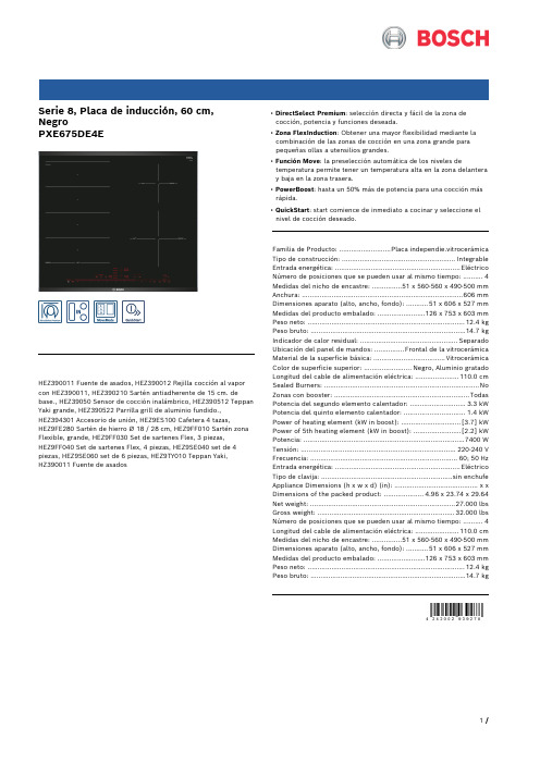
Serie 8, Placa de inducción, 60 cm,NegroPXE675DE4EHEZ390011 Fuente de asados, HEZ390012 Rejilla cocción al vapor con HEZ390011, HEZ390210 Sartén antiadherente de 15 cm. de base., HEZ39050 Sensor de cocción inalámbrico, HEZ390512 Teppan Yaki grande, HEZ390522 Parrilla grill de aluminio fundido.,HEZ394301 Accesorio de unión, HEZ9ES100 Cafetera 4 tazas,HEZ9FE280 Sartén de hierro Ø 18 / 28 cm, HEZ9FF010 Sartén zona Flexible, grande, HEZ9FF030 Set de sartenes Flex, 3 piezas,HEZ9FF040 Set de sartenes Flex, 4 piezas, HEZ9SE040 set de 4 piezas, HEZ9SE060 set de 6 piezas, HEZ9TY010 Teppan Yaki,HZ390011 Fuente de asados • DirectSelect Premium: selección directa y fácil de la zona decocción, potencia y funciones deseada.• Zona FlexInduction: Obtener una mayor flexibilidad mediante la combinación de las zonas de cocción en una zona grande para pequeñas ollas a utensilios grandes.• Función Move: la preselección automática de los niveles de temperatura permite tener un temperatura alta en la zona delantera y baja en la zona trasera.• PowerBoost: hasta un 50% más de potencia para una cocción más rápida.• QuickStart: start comience de inmediato a cocinar y seleccione el nivel de cocción deseado.Familia de Producto: ..........................Placa independie.vitrocerámica Tipo de construcción: .........................................................Integrable Entrada energética: ...............................................................Eléctrico Número de posiciones que se pueden usar al mismo tiempo: . (4)Medidas del nicho de encastre: ...............51 x 560-560 x 490-500 mm Anchura: .................................................................................606 mm Dimensiones aparato (alto, ancho, fondo): ...........51 x 606 x 527 mm Medidas del producto embalado: ........................126 x 753 x 603 mm Peso neto: ...............................................................................12.4 kg Peso bruto: ..............................................................................14.7 kg Indicador de calor residual: .................................................Separado Ubicación del panel de mandos: ...............Frontal de la vitrocerámica Material de la superficie básica: ....................................Vitrocerámica Color de superficie superior: ........................Negro, Aluminio gratado Longitud del cable de alimentación eléctrica: ......................110.0 cm Sealed Burners: ..............................................................................No Zonas con booster: ....................................................................Todas Potencia del segundo elemento calentador: ............................3.3 kW Potencia del quinto elemento calentador: ...............................1.4 kW Power of heating element (kW in boost): ..............................[3.7] kW Power of 5th heating element (kW in boost): ........................[2.2] kW Potencia: .................................................................................7400 W Tensión: ..............................................................................220-240 V Frecuencia: ..........................................................................60; 50 Hz Entrada energética: ...............................................................Eléctrico Tipo de clavija: ..................................................................sin enchufe Appliance Dimensions (h x w x d) (in): ..........................................x x Dimensions of the packed product: ....................4.96 x 23.74 x 29.64 Net weight: .........................................................................27.000 lbs Gross weight: .....................................................................32.000 lbs Número de posiciones que se pueden usar al mismo tiempo: . (4)Longitud del cable de alimentación eléctrica: ......................110.0 cm Medidas del nicho de encastre: ...............51 x 560-560 x 490-500 mm Dimensiones aparato (alto, ancho, fondo): ...........51 x 606 x 527 mm Medidas del producto embalado: ........................126 x 753 x 603 mm Peso neto: ...............................................................................12.4 kg Peso bruto: ..............................................................................14.7 kgSerie 8, Placa de inducción, 60 cm, NegroPXE675DE4EDiseño:- Terminación PremiumConfort:- 4 zonas de inducción- Direct Select 2.0- Regulación electrónica con 17 niveles de potencia- Programación de tiempo de cocción para cada zona y avisador acústico- Avisador acústico- STFE- Detección de recipiente- Posibilidad de limitar la potencia total de la encimera- Desconexión de seguridad de la placa- Bloqueo de seguridad para niños automático o manual- Función Clean: bloqueo temporal del control- Display de consumo de energíaSeguridad:- Indicador de calor residual dual (H/h)- Main SwitchPrestaciones profesionales- Sensor PerfectFry con 5 ajustes de temperaturaRapidez:- Función Sprint en todas las zonasSerie 8, Placa de inducción, 60 cm, NegroPXE675DE4E。
8286芯片

8286芯片
8286芯片是英特尔公司生产的一款高性能的芯片,它采用了
英特尔的14纳米制程工艺,拥有卓越的性能和低功耗特性。
下面将从性能、功耗、应用领域三个方面作详细介绍。
首先是性能方面,8286芯片拥有强大的计算能力和处理速度。
该芯片采用了先进的多核心架构,配备了高性能的处理器以及强大的图形处理单元,可以支持多线程处理和同时运行多个任务。
它具有出色的计算、图形渲染和多媒体处理能力,能够满足高性能计算、人工智能、游戏和视频编辑等需求。
其次是功耗方面,8286芯片采用了14纳米制程工艺,使得芯
片的功耗得到很好的控制。
它采用了新一代的低功耗设计,可以在保持高性能的同时降低功耗,延长电池寿命。
与之前的芯片相比,8286芯片在相同的工作负载下,能够提供更高的性能,同时保持较低的功耗。
最后是应用领域方面,8286芯片广泛应用于各个领域。
在数
据中心和云计算领域,它可以提供强大的计算和处理能力,为大规模数据处理和分析提供支持。
在移动设备领域,它可以提供卓越的图形渲染和多媒体处理能力,使得移动设备能够流畅播放高清视频和运行复杂的应用程序。
此外,8286芯片还可
以应用于人工智能领域,支持深度学习和机器学习等任务。
综上所述,8286芯片作为英特尔公司的一款高性能芯片,具
有出色的计算能力和处理速度,低功耗特性以及广泛的应用领域。
它的推出将为各行业的发展提供强有力的支持。
EP2C8Q208C8中文资料(Altera)中文数据手册「EasyDatasheet - 矽搜」
Cyclone II器件手册,第1卷ii内容章修订日期............................................... ............................喜关于本手册............................................... .............................十三如何触点Altera ..........................................................................................................................十三印刷约定....................................................................................................................十三第一节Cyclone II器件系列数据表修订记录.................................................................................................................................... 1-1第1章简介简介............................................................................................................................................低成本嵌入式处理解决方案............................................ ......................................低成本DSP解决方案.................................................................................................................特征...................................................................................................................................................参考文献.........................................................................................................................文档修订历史记录.................................................................................................................1–1 1–1 1–1 1–2 1–9 1–9第2章Cyclone II架构功能说明.......................................................................................................................... 2-1逻辑元件....................................................................................................................................... 2-2LE操作模式........................................................................................................................ 2-4逻辑阵列模块................................................................................................................................ 2-7LAB互连............................................................................................................................ 2-8LAB控制信号......................................................................................................................... 2-8MultiTrack互联..................................................................................................................... 2-10行互连.......................................................................................................................... 2-10列互连.................................................................................................................... 2-12设备路由............................................................................................................................... 2-15全局时钟网络和锁相环.......................................... ..................................... 2-16专用时钟管脚..................................................................................................................... 2-20双用时钟引脚.............................................................................................................. 2-20全局时钟网络................................................................................................................... 2-21全局时钟网络分布.............................................. .............................................. 2-23锁相环.................................................................................................................................................. 2-25嵌入式存储器............................................................................................................................. 2-27内存模式............................................................................................................................... 2-30时钟模式.................................................................................................................................... 2-31M4K路由接口.................................................................................................................. 2-31iii内容嵌入式乘法器........................................................................................................................乘法器模式............................................................................................................................嵌入式乘法器路由接口.............................................. .......................................I / O结构及特点....................................................................................................................外部存储器接口.......................................................................................................可编程驱动强度.....................................................................................................漏极开路输出........................................................................................................................摆率控制...........................................................................................................................总线防护持..........................................................................................................................................可编程上拉电阻............................................. .................................................. ...高级I / O标准支持............................................ .................................................. ..高速差分接口............................................. .................................................系列片上端接.........................................................................................................I / O组........................................................................................................................................多电压I / O接口.................................................................................................................2–32 2–35 2–36 2–37 2–44 2–49 2–50 2–51 2–51 2–51 2–52 2–53 2–55 2–57 2–60第3章配置与测试IEEE标准. 1149.1(JTAG)边界扫描支持........................................... ..................................构造.........................................................................................................................................操作模式...................................................................................................................................配置计划......................................................................................................................... Cyclone II自动单粒子翻转检测........................................... ...........................定制电路....................................................................................................................软件界面.............................................................................................................................文档修订历史记录.................................................................................................................3–1 3–5 3–5 3–6 3–7 3–7 3–7 3–8第4章热插拔和上电复位简介............................................................................................................................................旋风II热插拔规格............................................ ................................................设备可以在电源时会驱动.......................................... ...........................................I / O引脚防护持三态电期间...................................... ......................................在Cyclone II器件热插拔功能实现......................................... ..............上电复位电路...................................................................................................................."唤醒"时间Cyclone II器件........................................ ...............................................结论..............................................................................................................................................文档修订历史记录.................................................................................................................4–1 4–1 4–2 4–2 4–3 4–5 4–5 4–7 4–7第5章直流特性和时序规范运行条件........................................................................................................................... 5-1单端I / O标准.......................................................................................................... 5-5差分I / O标准.............................................................................................................. 5-7DC特性不同针类型............................................ ......................................... 5-11片上端接规格............................................. .............................................. 5-12能量消耗........................................................................................................................... 5-13时序规格.......................................................................................................................... 5-14预,决赛时序规范............................................. ................................ 5-14演出.................................................................................................................................... 5-15 ivCyclone II器件手册,第1卷内容内部时序...............................................................................................................................Cyclone II时钟时序参数............................................. ..............................................时钟网络偏移加法器.......................................................................................................IOE可编程延迟.............................................................................................................不同I默认容性负载/ O标准......................................... .................I / O延迟.......................................................................................................................................最大输入和输出时钟频率............................................ ........................................高速I / O时序规格........................................... ............................................外部存储器接口规范.............................................. ....................................JTAG时序规范..........................................................................................................PLL时序规范............................................................................................................占空比失真.........................................................................................................................DCD测量技术............................................... .................................................. ..参考文献.......................................................................................................................文档修订历史记录...............................................................................................................5–18 5–23 5–29 5–30 5–31 5–33 5–46 5–55 5–63 5–64 5–66 5–67 5–68 5–74 5–74第6章参考和订购信息软体..................................................................................................................................................器件引脚输出.....................................................................................................................................订购信息...........................................................................................................................文档修订历史记录.................................................................................................................6–1 6–1 6–1 6–2第二节.时钟管理修订记录.................................................................................................................................... 6-1第7章锁相环在Cyclone II器件简介............................................................................................................................................ 7-1Cyclone II PLL硬件概述............................................. .................................................. ... 7-2PLL参考时钟产生.............................................. .................................................. ... 7-6时钟反馈模式....................................................................................................................... 7-10正常模式.................................................................................................................................. 7-10零延迟缓冲器模式................................................................................................................ 7-11无补偿模式............................................................................................................... 7-12源同步模式........................................................................................................... 7-13硬件特性.............................................................................................................................. 7-14时钟倍频和科.............................................. .................................................. .. 7-14可编程占空比........................................................................................................... 7-15移相实施.............................................. .................................................. .... 7-16控制信号................................................................................................................................ 7-17手动时钟切换............................................................................................................. 7-20时钟................................................................................................................................................ 7-21全局时钟网络................................................................................................................... 7-21时钟控制模块....................................................................................................................... 7-24全局时钟网络时钟源产生............................................ .......................... 7-26全局时钟网络掉电............................................. .............................................. 7-28vCyclone II器件手册,第1卷。
Si4826DY资料
LM2727/LM2737N-Channel FET Synchronous Buck Regulator Controller for Low Output VoltagesGeneral DescriptionThe LM2727and LM2737are high-speed,synchronous,switching regulator controllers.They are intended to control currents of 0.7A to 20A with up to 95%conversion efficien-cies.The LM2727employs output over-voltage and under-voltage latch-off.For applications where latch-off is not de-sired,the LM2737can be used.Power up and down sequencing is achieved with the power-good flag,adjustable soft-start and output enable features.The LM2737and LM2737operate from a low-current 5V bias and can convert from a 2.2V to 16V power rail.Both parts utilize a fixed-frequency,voltage-mode,PWM control architecture and the switching frequency is adjustable from 50kHz to 2MHz by adjusting the value of an external resistor.Current limit is achieved by monitoring the voltage drop across the on-resistance of the low-side MOSFET,which enhances low duty-cycle operation.The wide range of operating frequen-cies gives the power supply designer the flexibility to fine-tune component size,cost,noise and efficiency.The adap-tive,non-overlapping MOSFET gate-drivers and high-side bootstrap structure helps to further maximize efficiency.The high-side power FET drain voltage can be from 2.2V to 16V and the output voltage is adjustable down to 0.6V.Featuresn Input power from 2.2V to 16Vn Output voltage adjustable down to 0.6Vn Power Good flag,adjustable soft-start and output enable for easy power sequencingn Output over-voltage and under-voltage latch-off (LM2727)n Output over-voltage and under-voltage flag (LM2737)n Reference Accuracy:1.5%(0˚C -125˚C)n Current limit without sense resistor n Soft startn Switching frequency from 50kHz to 2MHz n TSSOP-14packageApplicationsn Cable Modemsn Set-Top Boxes/Home Gateways n DDR Core Powern High-Efficiency Distributed Power nLocal Regulation of Core PowerTypical Application20049410June 2003LM2727/LM2737N-Channel FET Synchronous Buck Regulator Controller for Low Output Voltages©2003National Semiconductor Corporation Connection Diagram2004941114-Lead Plastic TSSOPθJA =155˚C/WNS Package Number MTC14Pin DescriptionBOOT (Pin 1)-Supply rail for the N-channel MOSFET gate drive.The voltage should be at least one gate threshold above the regulator input voltage to properly turn on the high-side N-FET.LG (Pin 2)-Gate drive for the low-side N-channel MOSFET.This signal is interlocked with HG to avoid shoot-through problems.PGND (Pins 3,13)-Ground for FET drive circuitry.It should be connected to system ground.SGND (Pin 4)-Ground for signal level circuitry.It should be connected to system ground.V CC (Pin 5)-Supply rail for the controller.PWGD (Pin 6)-Power Good.This is an open drain output.The pin is pulled low when the chip is in UVP ,OVP ,or UVLO mode.During normal operation,this pin is connected to V CC or other voltage source through a pull-up resistor.ISEN (Pin 7)-Current limit threshold setting.This sources a fixed 50µA current.A resistor of appropriate value should be connected between this pin and the drain of the low-side FET.EAO (Pin 8)-Output of the error amplifier.The voltage level on this pin is compared with an internally generated ramp signal to determine the duty cycle.This pin is necessary for compensating the control loop.SS (Pin 9)-Soft start pin.A capacitor connected between this pin and ground sets the speed at which the output voltage ramps rger capacitor value results in slower output voltage ramp but also lower inrush current.FB (Pin 10)-This is the inverting input of the error amplifier,which is used for sensing the output voltage and compen-sating the control loop.FREQ (Pin 11)-The switching frequency is set by connect-ing a resistor between this pin and ground.SD (Pin 12)-IC Logic Shutdown.When this pin is pulled low the chip turns off the high side switch and turns on the low side switch.While this pin is low,the IC will not start up.An internal 20µA pull-up connects this pin to V CC .HG (Pin 14)-Gate drive for the high-side N-channel MOS-FET.This signal is interlocked with LG to avoid shoot-through problems.L M 2727/L M 2737 2Absolute Maximum Ratings(Note1) If Military/Aerospace specified devices are required, please contact the National Semiconductor Sales Office/ Distributors for availability and specifications.V CC7V BOOTV21V Junction Temperature150˚C Storage Temperature−65˚C to150˚C Soldering InformationLead Temperature(soldering,10sec)260˚CInfrared or Convection(20sec)235˚C ESD Rating2kVOperating RatingsSupply Voltage(V CC) 4.5V to5.5V Junction Temperature Range−40˚C to+125˚C Thermal Resistance(θJA)155˚C/WElectrical CharacteristicsV CC=5V unless otherwise indicated.Typicals and limits appearing in plain type apply for T A=T J=+25˚C.Limits appearing in boldface type apply over full Operating Temperature Range.Datasheet min/max specification limits are guaranteed by design, test,or statistical analysis.Symbol Parameter Conditions Min Typ Max UnitsV FB_ADJ FB Pin Voltage V CC=4.5V,0˚C to+125˚C0.5910.60.609V V CC=5V,0˚C to+125˚C0.5910.60.609V CC=5.5V,0˚C to+125˚C0.5910.60.609V CC=4.5V,−40˚C to+125˚C0.5890.60.609V CC=5V,−40˚C to+125˚C0.5890.60.609V CC=5.5V,−40˚C to+125˚C0.5890.60.609V ON UVLO Thresholds RisingFalling 4.23.6VI Q-V5Operating V CC CurrentSD=5V,FB=0.55VFsw=600kHz1 1.52mASD=5V,FB=0.65VFsw=600kHz0.8 1.7 2.2 Shutdown V CC Current SD=0V0.150.40.7mAt PWGD1PWGD Pin Response Time FB Voltage Going Up6µs t PWGD2PWGD Pin Response Time FB Voltage Going Down6µs I SD SD Pin Internal Pull-up Current20µA I SS-ON SS Pin Source Current SS Voltage=2.5V0˚C to+125˚C -40˚C to+125˚C 8511111515µAI SS-OC SS Pin Sink Current During OverCurrent SS Voltage=2.5V95µAI SEN-TH I SEN Pin Source Current TripPoint0˚C to+125˚C-40˚C to+125˚C352850506565µAERROR AMPLIFIERGBW Error Amplifier Unity GainBandwidth5MHzG Error Amplifier DC Gain60dBSR Error Amplifier Slew Rate6V/µAI FB FB Pin Bias Current FB=0.55VFB=0.65V 01530100155nAI EAO EAO Pin Current Sourcing andSinking V EAO=2.5,FB=0.55VV EAO=2.5,FB=0.65V2.80.8mAV EA Error Amplifier Maximum Swing MinimumMaximum1.23.2VLM2727/LM27373Electrical Characteristics(Continued)V CC =5V unless otherwise indicated.Typicals and limits appearing in plain type apply for T A =T J =+25˚C.Limits appearing in boldface type apply over full Operating Temperature Range.Datasheet min/max specification limits are guaranteed by design,test,or statistical analysis.SymbolParameterConditionsMinTypMaxUnitsGATE DRIVE I Q-BOOTBOOT Pin Quiescent CurrentBOOTV =12V,EN =00˚C to +125˚C -40˚C to +125˚C 9595160215µAR DS1Top FET Driver Pull-Up ON resistanceBOOT-SW =5V @350mA 3ΩR DS2Top FET Driver Pull-Down ON resistanceBOOT-SW =5V @350mA 2ΩR DS3Bottom FET Driver Pull-Up ON resistanceBOOT-SW =5V @350mA 3ΩR DS4Bottom FET Driver Pull-Down ON resistanceBOOT-SW =5V @350mA2ΩOSCILLATORf OSCPWM FrequencyR FADJ =590k Ω50kHzR FADJ =88.7k Ω300R FADJ =42.2k Ω,0˚C to +125˚C 500600700R FADJ =42.2k Ω,-40˚C to +125˚C 490600700R FADJ =17.4k Ω1400R FADJ =11.3k Ω2000DMax Duty Cyclef PWM =300kHz f PWM =600kHz9088%LOGIC INPUTS AND OUTPUTSV SD-IH SD Pin Logic High Trip Point 2.63.5V V SD-IL SD Pin Logic Low Trip Point 0˚C to +125˚C -40˚C to +125˚C 1.31.25 1.61.6VV PWGD-TH-LOPWGD Pin Trip PointsFB Voltage Going Down 0˚C to +125˚C -40˚C to +125˚C 0.4130.4100.4300.4300.4460.446VV PWGD-TH-HIPWGD Pin Trip PointsFB Voltage Going Up 0˚C to +125˚C -40˚C to +125˚C0.6910.6880.7100.7100.7340.734VV PWGD-HYSPWGD Hysteresis (LM2737only)FB Voltage Going Down FB VoltageGoing Up35110mVNote 1:Absolute maximum ratings indicate limits beyond which damage to the device may occur.Operating ratings indicate conditions for which the device operates correctly.Opearting Ratings do not imply guaranteed performance limits.Note 2:The human body model is a 100pF capacitor discharged through a 1.5k resistor into each pin.L M 2727/L M 2737 4Typical Performance CharacteristicsEfficiency (V O =1.5V)F SW =300kHz,T A =25˚CEfficiency (V O =3.3V)F SW =300kHz,T A =25˚C2004941220049413V CC Operating Current vs TemperatureF SW =600kHz,No-Load Bootpin Current vs Temperature for BOOTV =12VF SW =600kHz,Si4826DY FET,No-Load2004941420049415Bootpin Current vs Temperature with 5V BootstrapF SW =600kHz,Si4826DY FET,No-Load PWM Frequency vs Temperaturefor R FADJ =43.2k Ω2004941620049417LM2727/LM27375Typical Performance Characteristics(Continued)R FADJ vs PWM Frequency(in 100to 800kHz range),T A =25˚CR FADJ vs PWM Frequency(in 900to 2000kHz range),T A =25˚C2004941820049419V CC Operating Current Plus Boot Current vs PWM Frequency (Si4826DY FET,T A =25˚C)Switch Waveforms (HG Falling)V IN =5V,V O =1.8V I O =3A,C SS =10nF F SW =600kHz2004942020049423Switch Waveforms (HG Rising)V IN =5V,V O =1.8V I O =3A,F SW =600kHzStart-Up (No-Load)V IN =10V,V O =1.2V C SS =10nF,F SW =300kHz2004942420049421L M 2727/L M 2737 6Typical Performance Characteristics(Continued)Start-Up (Full-Load)V IN =10V,V O =1.2V I O =10A,C SS =10nFF SW =300kHzStart Up (No-Load,10x C SS )V IN =10V,V O =1.2V C SS =100nF,F SW =300kHz2004942220049426Start Up (Full Load,10x C SS )V IN =10V,V O =1.2V I O =10A,C SS =100nFF SW =300kHz ShutdownV IN =10V,V O =1.2V I O =10A,C SS =10nFF SW =300kHz2004942520049427Start Up (Full Load,10x C SS )V IN =10V,V O =1.2V I O =10A,C SS =100nFF SW =300kHzLoad Transient Response (I O =0to 4A)V IN =12V,V O =1.2VF SW =300kHz2004943320049428LM2727/LM27377Typical Performance Characteristics(Continued)Load Transient Response (I O =4to 0A)V IN =12V,V O =1.2VF SW =300kHzLine Transient Response (V IN =5V to 12V)V O =1.2V,I O =5A F SW =300kHz2004942920049430Line Transient Response (V IN =12V to 5V)V O =1.2V,I O =5A F SW =300kHz Line Transient ResponseV O =1.2V,I O =5A F SW =300kHz2004943120049432L M 2727/L M 2737 8Block Diagram20049401Application InformationTHEORY OF OPERATIONThe LM2727is a voltage-mode,high-speed synchronous buck regulator with a PWM control scheme.It is designed for use in set-top boxes,thin clients,DSL/Cable modems,and other applications that require high efficiency buck convert-ers.It has power good (PWRGD),output shutdown (SD),over voltage protection (OVP)and under voltage protection (UVP).The over-voltage and under-voltage signals are OR gated to drive the Power Good signal and a shutdown latch,which turns off the high side gate and turns on the low side gate if pulled low.Current limit is achieved by sensing the voltage V DS across the low side FET.During current limit the high side gate is turned off and the low side gate turned on.The soft start capacitor is discharged by a 95µA source (reducing the maximum duty cycle)until the current is under control.The LM2737does not latch off during UVP or OVP ,and uses the HIGH and LOW comparators for the power-good function only.START UPWhen V CC exceeds 4.2V and the enable pin EN sees a logic high the soft start capacitor begins charging through an internal fixed 10µA source.During this time the output of the error amplifier is allowed to rise with the voltage of the soft start capacitor.This capacitor,Css,determines soft start time,and can be determined approximately by:An application for a microprocessor might need a delay of 3ms,in which case C SS would be 12nF.For a different device,a 100ms delay might be more appropriate,in which case C SS would be 400nF.(39010%)During soft start the PWRGD flag is forced low and is released when the voltage reaches a set value.At this point this chip enters normal operation mode,the Power Good flag is released,and the OVP and UVP functions begin to monitor Vo.NORMAL OPERATIONWhile in normal operation mode,the LM2727/37regulates the output voltage by controlling the duty cycle of the high side and low side FETs.The equation governing output voltage is:The PWM frequency is adjustable between 50kHz and 2MHz and is set by an external resistor,R FADJ ,between the FREQ pin and ground.The resistance needed for a desired frequency is approximately:LM2727/LM27379Application Information(Continued)MOSFET GATE DRIVERSThe LM2727/37has two gate drivers designed for driving N-channel MOSFETs in a synchronous mode.Power for the drivers is supplied through the BOOTV pin.For the high side gate (HG)to fully turn on the top FET,the BOOTV voltage must be at least one V GS(th)greater than Vin.(BOOTV ≥2*Vin)This voltage can be supplied by a separate,higher voltage source,or supplied from a local charge pump struc-ture.In a system such as a desktop computer,both 5V and 12V are usually available.Hence if Vin was 5V,the 12V supply could be used for BOOTV.12V is more than 2*Vin,so the HG would operate correctly.For a BOOTV of 12V,the initial gate charging current is 2A,and the initial gate dis-charging current is typically 6A.In a system without a separate,higher voltage,a charge pump (bootstrap)can be built using a diode and small ca-pacitor,Figure 1.The capacitor serves to maintain enough voltage between the top FET gate and source to control the device even when the top FET is on and its source has risen up to the input voltage level.The LM2727/37gate drives use a BiCMOS design.Unlike some other bipolar control ICs,the gate drivers have rail-to-rail swing,ensuring no spurious turn-on due to capacitive coupling.POWER GOOD SIGNALThe power good signal is the or-gated flag representing over-voltage and under-voltage protection.If the output volt-age is 18%over it’s nominal value,V FB =0.7V,or falls 30%below that value,V FB =0.41V,the power good flag goes low.The converter then turns off the high side gate,and turns on the low side gate.Unlike the output (LM2727only)the power good flag is not latched off.It will return to a logic high whenever the feedback pin voltage is between 70%and 118%of 0.6V.UVLOThe 4.2V turn-on threshold on V CC has a built in hysteresis of 0.6V.Therefore,if V CC drops below 3.6V,the chip enters UVLO mode.UVLO consists of turning off the top FET,turning on the bottom FET,and remaining in that conditionuntil V CC rises above 4.2V.As with shutdown,the soft start capacitor is discharged through a FET,ensuring that the next start-up will be smooth.CURRENT LIMITCurrent limit is realized by sensing the voltage across the low side FET while it is on.The R DSON of the FET is a known value,hence the current through the FET can be determined as:V DS =I *R DSON The current limit is determined by an external resistor,R CS ,connected between the switch node and the ISEN pin.A constant current of 50µA is forced through Rcs,causing a fixed voltage drop.This fixed voltage is compared against V DS and if the latter is higher,the current limit of the chip has been reached.R CS can be found by using the following:R CS =R DSON (LOW)*I LIM /50µAFor example,a conservative 15A current limit in a 10A design with a minimum R DSON of 10m Ωwould require a 3.3k Ωresistor.Because current sensing is done across the low side FET,no minimum high side on-time is necessary.In the current limit mode the LM2727/37will turn the high side off and the keep low side on for as long as necessary.The chip also discharges the soft start capacitor through a fixed 95µA source.In this way,smooth ramping up of the output voltage as with a normal soft start is ensured.The output of the LM2727/37internal error amplifier is limited by the volt-age on the soft start capacitor.Hence,discharging the soft start capacitor reduces the maximum duty cycle D of the controller.During severe current limit,this reduction in duty cycle will reduce the output voltage,if the current limit con-ditions lasts for an extended time.During the first few nanoseconds after the low side gate turns on,the low side FET body diode conducts.This causes an additional 0.7V drop in V DS .The range of V DS is normally much lower.For example,if R DSON were 10m Ωand the current through the FET was 10A,V DS would be 0.1V.The current limit would see 0.7V as a 70A current and enter current limit immediately.Hence current limit is masked dur-ing the time it takes for the high side switch to turn off and the low side switch to turn on.UVP/OVPThe output undervoltage protection and overvoltage protec-tion mechanisms engage at 70%and 118%of the target output voltage,respectively.In either case,the LM2727will turn off the high side switch and turn on the low side switch,and discharge the soft start capacitor through a MOSFET switch.The chip remains in this state until the shutdown pin has been pulled to a logic low and then released.The UVP function is masked only during the first charging of the soft start capacitor,when voltage is first applied to the V CC pin.In contrast,the LM2737is designed to continue operating dur-ing UVP or OVP conditions,and to resume normal operation once the fault condition is cleared.As with the LM2727,the powergood flag goes low during this time,giving a logic-level warning signal.SHUT DOWNIf the shutdown pin SD is pulled low,the LM2727/37dis-charges the soft start capacitor through a MOSFET switch.The high side switch is turned off and the low side switch is turned on.The LM2727/37remains in this state until SD is released.20049402FIGURE 1.BOOTV Supplied by Charge Pump L M 2727/L M 2737 10Application Information(Continued)DESIGN CONSIDERATIONSThe following is a design procedure for all the componentsneeded to create the circuit shown in Figure3in the Ex-ample Circuits section,a5V in to1.2V out converter,capableof delivering10A with an efficiency of85%.The switchingfrequency is300kHz.The same procedures can be followedto create the circuit shown in Figure3,Figure4,and tocreate many other designs with varying input voltages,out-put voltages,and output currents.INPUT CAPACITORThe input capacitors in a Buck switching converter are sub-jected to high stress due to the input current waveform,which is a square wave.Hence input caps are selected fortheir ripple current capability and their ability to withstand theheat generated as that ripple current runs through their ESR.Input rms ripple current is approximately:The power dissipated by each input capacitor is:Here,n is the number of capacitors,and indicates that powerloss in each cap decreases rapidly as the number of inputcaps increase.The worst-case ripple for a Buck converteroccurs during full load,when the duty cycle D=50%.In the5V to 1.2V case,D= 1.2/5=0.24.With a10Amaximum load the ripple current is 4.3A.The Sanyo10MV5600AX aluminum electrolytic capacitor has a ripplecurrent rating of2.35A,up to105˚C.Two such capacitorsmake a conservative design that allows for unequal currentsharing between individual caps.Each capacitor has a maxi-mum ESR of18mΩat100kHz.Power loss in each device isthen0.05W,and total loss is0.1W.Other possibilities forinput and output capacitors include MLCC,tantalum,OSCON,SP,and POSCAPS.INPUT INDUCTORThe input inductor serves two basic purposes.First,in highpower applications,the input inductor helps insulate theinput power supply from switching noise.This is especiallyimportant if other switching converters draw current from thesame supply.Noise at high frequency,such as that devel-oped by the LM2727at1MHz operation,could pass throughthe input stage of a slower converter,contaminating andpossibly interfering with its operation.An input inductor also helps shield the LM2727from highfrequency noise generated by other switching converters.The second purpose of the input inductor is to limit the inputcurrent slew rate.During a change from no-load to full-load,the input inductor sees the highest voltage change across it,equal to the full load current times the input capacitor ESR.This value divided by the maximum allowable input currentslew rate gives the minimum input inductance:In the case of a desktop computer system,the input currentslew rate is the system power supply or"silver box"outputcurrent slew rate,which is typically about0.1A/µs.Total inputcapacitor ESR is9mΩ,hence∆V is10*0.009=90mV,andthe minimum inductance required is0.9µH.The input induc-tor should be rated to handle the DC input current,which isapproximated by:In this case I IN-DC is about2.8A.One possible choice is theTDK SLF12575T-1R2N8R2,a1.2µH device that can handle8.2Arms,and has a DCR of7mΩ.OUTPUT INDUCTORThe output inductor forms the first half of the power stage ina Buck converter.It is responsible for smoothing the squarewave created by the switching action and for controlling theoutput current ripple.(∆I o)The inductance is chosen byselecting between tradeoffs in efficiency and response time.The smaller the output inductor,the more quickly the con-verter can respond to transients in the load current.Asshown in the efficiency calculations,however,a smaller in-ductor requires a higher switching frequency to maintain thesame level of output current ripple.An increase in frequencycan mean increasing loss in the FETs due to the chargingand discharging of the gates.Generally the switching fre-quency is chosen so that conduction loss outweighs switch-ing loss.The equation for output inductor selection is:Plugging in the values for output current ripple,input voltage,output voltage,switching frequency,and assuming a40%peak-to-peak output current ripple yields an inductance of1.5µH.The output inductor must be rated to handle the peakcurrent(also equal to the peak switch current),which is(Io+0.5*∆I o).This is12A for a10A design.The Coilcraft D05022-152HC is1.5µH,is rated to15Arms,and has a DCR of4mΩ.OUTPUT CAPACITORThe output capacitor forms the second half of the powerstage of a Buck switching converter.It is used to control theoutput voltage ripple(∆V o)and to supply load current duringfast load transients.In this example the output current is10A and the expectedtype of capacitor is an aluminum electrolytic,as with theinput capacitors.(Other possibilities include ceramic,tanta-lum,and solid electrolyte capacitors,however the ceramictype often do not have the large capacitance needed tosupply current for load transients,and tantalums tend to bemore expensive than aluminum electrolytic.)Aluminum ca-pacitors tend to have very high capacitance and fairly lowESR,meaning that the ESR zero,which affects systemstability,will be much lower than the switching frequency.The large capacitance means that at switching frequency,the ESR is dominant,hence the type and number of outputcapacitors is selected on the basis of ESR.One simpleformula to find the maximum ESR based on the desiredoutput voltage ripple,∆V o and the designed output currentripple,∆I o,is:LM2727/LM2737Application Information(Continued)In this example,in order to maintain a 2%peak-to-peak output voltage ripple and a 40%peak-to-peak inductor cur-rent ripple,the required maximum ESR is 6m Ω.Three Sanyo 10MV5600AX capacitors in parallel will give an equivalent ESR of 6m Ω.The total bulk capacitance of 16.8mF is enough to supply even severe load ing the same capacitors for both input and output also keeps the bill of materials simple.MOSFETSMOSFETS are a critical part of any switching controller and have a direct impact on the system efficiency.In this case the target efficiency is 85%and this is the variable that will determine which devices are acceptable.Loss from the ca-pacitors,inductors,and the LM2727itself are detailed in the Efficiency section,and come to about 0.54W.To meet the target efficiency,this leaves 1.45W for the FET conduction loss,gate charging loss,and switching loss.Switching loss is particularly difficult to estimate because it depends on many factors.When the load current is more than about 1or 2amps,conduction losses outweigh the switching and gate charging losses.This allows FET selection based on the R DSON of the FET.Adding the FET switching and gate-charging losses to the equation leaves 1.2W for conduction losses.The equation for conduction loss is:P Cnd =D(I 2o *R DSON *k)+(1-D)(I 2o *R DSON *k)The factor k is a constant which is added to account for the increasing R DSON of a FET due to heating.Here,k =1.3.The Si4442DY has a typical R DSON of 4.1m Ω.When plugged into the equation for P CND the result is a loss of 0.533W.If this design were for a 5V to 2.5V circuit,an equal number of FETs on the high and low sides would be the best solution.With the duty cycle D =0.24,it becomes apparent that the low side FET carries the load current 76%of the time.Adding a second FET in parallel to the bottom FET could improve the efficiency by lowering the effective R DSON .The lower the duty cycle,the more effective a second or even third FET can be.For a minimal increase in gate charging loss (0.054W)the decrease in conduction loss is 0.15W.What was an 85%design improves to 86%for the added cost of one SO-8MOSFET.CONTROL LOOP COMPONENTSThe circuit is this design example and the others shown in the Example Circuits section have been compensated to improve their DC gain and bandwidth.The result of this compensation is better line and load transient responses.For the LM2727,the top feedback divider resistor,Rfb2,is also a part of the compensation.For the 10A,5V to 1.2V design,the values are:Cc1=4.7pF 10%,Cc2=1nF 10%,Rc =229k Ω1%.These values give a phase margin of 63˚and a bandwidth of 29.3kHz.SUPPORT CAPACITORS AND RESISTORSThe Cinx capacitors are high frequency bypass devices,designed to filter harmonics of the switching frequency and input noise.Two 1µF ceramic capacitors with a sufficient voltage rating (10V for the Circuit of Figure 3)will work well in almost any case.Rbypass and Cbypass are standard filter components de-signed to ensure smooth DC voltage for the chip supply and for the bootstrap structure,if it is e 10Ωfor the resistor and a 2.2µF ceramic for the cap.Cb is the bootstrap capacitor,and should be 0.1µF.(In the case of a separate,higher supply to the BOOTV pin,this 0.1µF cap can be used to bypass the supply.)Using a Schottky device for the boot-strap diode allows the minimum drop for both high and low side drivers.The On Semiconductor BAT54or MBR0520work well.Rp is a standard pull-up resistor for the open-drain power good signal,and should be 10k Ω.If this feature is not necessary,it can be omitted.R CS is the resistor used to set the current limit.Since the design calls for a peak current magnitude (Io +0.5*∆I o )of 12A,a safe setting would be 15A.(This is well below the saturation current of the output inductor,which is 25A.)Following the equation from the Current Limit section,use a 3.3k Ωresistor.R FADJ is used to set the switching frequency of the chip.Following the equation in the Theory of Operation section,the closest 1%tolerance resistor to obtain f SW =300kHz is 88.7k Ω.C SS depends on the users requirements.Based on the equation for C SS in the Theory of Operation section,for a 3ms delay,a 12nF capacitor will suffice.EFFICIENCY CALCULATIONSA reasonable estimation of the efficiency of a switching controller can be obtained by adding together the loss is each current carrying element and using the equation:The following shows an efficiency calculation to complement the Circuit of Figure 3.Output power for this circuit is 1.2V x 10A =12W.Chip Operating LossP IQ =I Q-V CC *V CC2mA x 5V =0.01WFET Gate Charging LossP GC =n *V CC *Q GS *f OSCThe value n is the total number of FETs used.The Si4442DY has a typical total gate charge,Q GS ,of 36nC and an r ds-on of 4.1m Ω.For a single FET on top and bottom:2*5*36E -9*300,000=0.108W FET Switching LossP SW =0.5*V in *I O *(t r +t f )*f OSC The Si4442DY has a typical rise time t r and fall time t f of 11and 47ns,respectively.0.5*5*10*58E -9*300,000=0.435WL M 2727/L M 2737。
AD8226中文资料

Wide Supply Range, Rail-to-RailRev. PrAInformation furnished by Analog Devices is believed to be accurate and reliable. However, noresponsibility is assumed by Analog Devices for its use, nor for any infringements of patents or other rights of third parties that may result from its use. Specifications subject to change without notice. No license is granted by implication or otherwise under any patent or patent rights of Analog Devices. T rademarks and registered trademarks are the property of their respective owners. One Technology Way, P.O. Box 9106, Norwood, MA 02062-9106, U.S.A. Tel: 781.329.4700 Fax: 781.461.3113 ©2008 Analog Devices, Inc. All rights reserved.FEATURESGain set with 1 external resistor Gain range: 1 to 1000Input voltage goes to ground Input overdrive protection Very wide power supply range Dual supply: ±1.3 V to ±18 V Single supply: 2.6 V to 36 V Bandwidth (G = 1): 800 kHz CMRR (G = 1): 78 dB minimum Input noise: 22 nV/rt(Hz) Typical supply current: 350 µA SOIC-8 and MSOP-8 packages APPLICATIONSIndustrial process controls Bridge amplifiersMedical instrumentation Portable data acquisition Multichannel systemsTOP VIEW(Not to Scale)736-1–INR GR G+IN+V SV OUTREF–V SFigure 1.GENERAL DESCRIPTIONThe AD8226 is a low cost instrumentation amplifier that requiresonly one external resistor to set any gain between 1 and 1000. The AD8226 is designed to work with a very wide range of voltages. It can operate on supplies ranging from ±1.2 V to±18 V (2.4 V to 36 V single supply). The AD8226 comes with rail-to-rail output and a wide input range that includes the ability to go slightly below the negative supply. In addition, the AD8226 inputs can withstand voltages beyond the rail.The AD8226 is perfect for multichannel, space-constrained applications. Being a low power and low cost amplifier allows multiple channels to be used.The AD8226 has three grades. The A grade is the lower cost version and is specified for temperatures from −40°C to +85°C. The B grade is the higher performance version and is specified from −40°C to +85°C. The C grade version is the higher temperature version and is specified from −40°C to +105°C. All models are operational from −40°C to +125°C; behavior at these temperatures is shown in the typical performance curves. The AD8226 is available in MSOP and SOIC packages.1Rail-to-rail output.Rev. PrA | Page 2 of 16TABLE OF CONTENTSFeatures .............................................................................................. 1 Applications ....................................................................................... 1 Pin Configuration ............................................................................. 1 General Description ......................................................................... 1 Specifications ..................................................................................... 3 Absolute Maximum Ratings ............................................................ 7 Thermal Resistance ...................................................................... 7 ESD Caution .................................................................................. 7 Pin Configuration and Function Descriptions ............................. 8 Theory of Operation ........................................................................ 9 Architecture ...................................................................................9 Gain Selection ................................................................................9 Input Protection ............................................................................9 Reference Terminal .................................................................... 10 Input Voltage Range ................................................................... 10 Layout .......................................................................................... 10 Input Bias Current Return Path ............................................... 11 Radio Frequency Interference (RFI) ........................................ 11 Outline Dimensions ....................................................................... 12 Ordering Guide .. (13)SPECIFICATIONS+V S = +15 V, −V S = −15 V, V REF = 0 V, T A = 25°C, G = 1, R L = 10 kΩ, unless otherwise noted.Rev. PrA | Page 3 of 16Rev. PrA | Page 4 of 161 Does not include the effects of external resistor R G2Input voltage range of the AD8226 input stage. Input range depends on common mode voltage, differential voltage, gain, and reference voltage. See the Input Voltage Range section in the Theory of Operation for more information.+V S = 2.7 V, –V S = 0 V, V REF = 0 V, T A = 25°C, G = 1, R L = 10 kΩ, unless otherwise noted.Rev. PrA | Page 5 of 16Rev. PrA | Page 6 of 161 Does not include the effects of external resistor R G2Input voltage range of the AD8226 input stage. Input range depends on common mode voltage, differential voltage, gain, and reference voltage. See the Input Voltage Range section in the Theory of Operation for more information.Rev. PrA | Page 7 of 16ABSOLUTE MAXIMUM RATINGS1Temperature range for specified performance is either −40°C to +85°C or −40°C to +105°C, depending on grade.Stresses above those listed under Absolute Maximum Ratings may cause permanent damage to the device. This is a stress rating only; functional operation of the device at these or any other conditions above those indicated in the operationalsection of this specification is not implied. Exposure to absolute maximum rating conditions for extended periods may affect device reliability. THERMAL RESISTANCEθJA is specified for a device in free air.Rev. PrA | Page 8 of 16PIN CONFIGURATION AND FUNCTION DESCRIPTIONSTOP VIEW (Not to Scale)07036-002–INR G R G +IN+V S V OUT REF –V SFigure 2. Pin ConfigurationRev. PrA | Page 9 of 16THEORY OF OPERATION07036-003AMPLIFIER STAGEGAIN STAGEFigure 3. Simplified SchematicARCHITECTUREThe AD8226 is based on the classic three op amp topology. This topology has two stages: a preamplifier to provide differential amplification, followed by a difference amplifier to remove the common-mode voltage. Figure 3 shows a simplified schematic of the AD8226.The first stage works as follows: in order to maintain a constant voltage across the Bias Resistor R B , Amplifier A1 must keep Node 3 a constant diode drop above the positive input voltage. Similarly, Amplifier A2 keeps Node 4 at a constant diode drop above the negative input voltage. Therefore a replica of the differential input voltage is placed across the gain setting resistor, R G . The current that flows across this resistance must also flow through the R1 and R2 resistors, creating a gained differential signal between the A2 and A1 outputs. Note that, in addition to a gained differential signal, the original common-mode signal, shifted a diode drop down, is also still present. The second stage is a difference amplifier, composed of A3 and four 50 kΩ resistors. The purpose of this stage is to remove the common-mode signal from the amplified differential signal. Because the input amplifiers employ a current feedback architecture, the gain-bandwidth product of the AD8226 increases with gain, resulting in a system that does not suffer from the expected bandwidth loss of voltage feedback architectures at higher gains.The transfer function of the AD8226 isV OUT = G (V IN+ − V IN−) + V REF whereGR G kΩ49.41+=GAIN SELECTIONPlacing a resistor across the R G terminals sets the gain of the AD8226, which can be calculated by referring to Table 7 or by using the following gain equation:1kΩ49.4−=G R GThe AD8226 defaults to G = 1 when no gain resistor is used. The tolerance and gain drift of the R G resistor should be added to the AD8226’s specifications to determine the total gain accuracy of the system. When the gain resistor is not used, gain error and gain drift are minimal.INPUT PROTECTIONThe input terminals of the AD8226 have input protection that allows the input voltage to go beyond the rails without damaging the part. Maximum voltage is –Vs+40 V and minimum voltage is +Vs-40 V . For example: with ±15 Vsupplies, the part can withstand input voltages of ±25 V; with a 5 V single supply, maximum input voltage is 40 V and minimum input voltage is 35 V .Rev. PrA | Page 10 of 16REFERENCE TERMINALThe output voltage of the AD8226 is developed with respect to the potential on the reference terminal. This is useful when the output signal needs to be offset to a precise midsupply level. For example, a voltage source can be tied to the REF pin to level-shift the output so that the AD8226 can drive a single-supply ADC. The REF pin is protected with ESD diodes and should not exceed either +V S or −V S by more than 0.3 V .For the best performance, source impedance to the REFterminal should be kept below 2 Ω. As shown in Figure 3, the reference terminal, REF, is at one end of a 50 kΩ resistor. Additional impedance at the REF terminal adds to this 50 kΩ resistor and results in amplification of the signal connected to the positive input. The amplification from the additional R REF can be computed by 2(50 kΩ + R REF )/100 kΩ + R REF . Only the positive signal path is amplified; the negative path is unaffected. This uneven amplification degrades CMRR.INCORRECTCORRECTFigure 4. Driving the Reference PinINPUT VOLTAGE RANGEThe three op amp architecture of the AD8226 applies gain in the first stage before removing common-mode voltage in the difference amplifier stage. In addition, the input transistors in the first stage shift the common mode voltage up one diode drop (about 650 mV .) Therefore, internal nodes between the first and second stages (nodes 1 and 2 in Figure 3) experience a combination of gained signal, common-mode signal, and 650 mV . This combined signal can be limited by the voltage supplies even when the individual input and output signals are not. Figure XX through Figure XX show the allowablecommon-mode input voltage ranges for various output voltages and supply voltages.The following formulas can also be used to understand how the reference voltage (V REF ), common mode input voltage (V CM ), and differential input voltage (V DIFF ) interact. These twoformulas, along with the input range specifications in Table 1 and Table 3, set the boundaries where the part operates with best performance.V 9.02))((V 4.0−+<+<−−S CM DIFF S V V GAIN V VVV V V GAIN V S REFCM DIFF .6122))((−+<++The common-mode input range shifts upwards with temper-ature. At cold temperatures, the part requires an extra 200 mV of headroom from the positive supply, and operation near the negative supply has more margin. Conversely, hot temperatures require less headroom from the positive supply, but are the worst-case conditions for input voltages near the negative supply.LAYOUTTo ensure optimum performance of the AD8226 at the PCB level, care must be taken in the design of the board layout. The AD8226 pins are arranged in a logical manner to aid in this task.–IN R G R G S OUT S+IN (Not to Scale)07036-005Figure 5. Pinout DiagramCommon-Mode Rejection Ratio over FrequencyPoor layout can cause some of the common-mode signals to be converted to differential signals before reaching the in-amp. Such conversions occur when one input path has a frequency response that is different from the other. To keep CMRR across frequency high, input source impedance and capacitance of each path should be closely matched. Additional source resistance in the input path (for example, for input protection) should be placed close to the in-amp inputs, which minimizes their interaction with parasitic capacitance from the PCB traces.Parasitic capacitance at the gain setting pins can also affect CMRR over frequency. If the board design has a component at the gain setting pins (for example, a switch or jumper), the part should be chosen so that the parasitic capacitance is as small as possible.Power SuppliesA stable dc voltage should be used to power the instrumenta-tion amplifier. Noise on the supply pins can adversely affect performance.A 0.1 µF capacitor should be placed as close as possible to each supply pin. As shown in Figure 6, a 10 µF tantalum capacitor can be used farther away from the part. In most cases, it can be shared by other precision integrated circuits.+VFigure 6. Supply Decoupling, REF, and Output Referred to Local GroundReferencesThe output voltage of the AD8226 is developed with respect to the potential on the reference terminal. Care should be taken to tie REF to the appropriate local ground.INPUT BIAS CURRENT RETURN PATHThe input bias current of the AD8226 must have a return path to ground. When the source, such as a thermocouple, cannot provide a return current path, one should be created, as shown in Figure 7.THERMOCOUPLE–VSCAPACITIVELY COUPLED +V SREFCC–V S AD8226TRANSFORMER+V SREF–VSAD8226INCORRECTCAPACITIVELY COUPLEDf HIGH-PASSTHERMOCOUPLETRANSFORMER–V SCORRECT07036-007Figure 7. Creating an I BIAS PathRADIO FREQUENCY INTERFERENCE (RFI)RF rectification is often a problem when amplifiers are used in applications having strong RF signals. The disturbance can appear as a small dc offset voltage. High frequency signals can be filtered with a low-pass RC network placed at the input of the instru-mentation amplifier, as shown in Figure 8. The filter limits the input signal bandwidth, according to the following relationship:FilterFrequency DIFF =)2(π21C D C C R +FilterFrequency CM = CRC π21where C D ≥ 10 C C .+V 07036-008Figure 8. RFI SuppressionC D affects the difference signal, and C C affects the common-mode signal. Values of R and C C should be chosen to minimize RFI. Mismatch between the R × C C at the positive input and the R × C C at the negative input degrades the CMRR of the AD8226. By using a value of C D one magnitude larger than C C , the effect of the mismatch is reduced, and performance is improved.OUTLINE DIMENSIONSCOMPLIANT TO JEDEC STANDARDS MO-187-AA0.800.600.40PLANE0.10Figure 9. 8-Lead Mini Small Outline Package [MSOP](RM-8)Dimensions shown in millimetersCONTROLLING DIMENSIONS ARE IN MILLIMETERS; INCH DIMENSIONS (IN PARENTHESES)ARE ROUNDED-OFF MILLIMETER EQUIVALENTS FOR REFERENCE ONLY AND ARE NOT APPROPRIATE FOR USE IN DESIGN.COMPLIANT TO JEDEC STANDARDS MS-012-AA012407-A0.17 (0.0067)0.25 (0.0098)0.10 (0.0040)COPLANARITY0.10Figure 10. 8-Lead Standard Small Outline Package [SOIC_N]Narrow Body(R-8)Dimensions shown in millimeters and (inches)1 Z = RoHS Compliant Part.NOTESNOTES元器件交易网AD8226 Preliminary Technical Data NOTES©2008 An alog Devices, In c. All rights reserved. Trademarks an dregistered trademarks are the property of their respective own ers.PR07036-0-10/08(PrA)。
- 1、下载文档前请自行甄别文档内容的完整性,平台不提供额外的编辑、内容补充、找答案等附加服务。
- 2、"仅部分预览"的文档,不可在线预览部分如存在完整性等问题,可反馈申请退款(可完整预览的文档不适用该条件!)。
- 3、如文档侵犯您的权益,请联系客服反馈,我们会尽快为您处理(人工客服工作时间:9:00-18:30)。
®82C86HCMOS Octal Bus TransceiverFN2977.2June 2004Features•Full Eight Bit Bi-Directional Bus Interface •Industry Standard 8286 Compatible Pinout•High Drive Capability-B Side I OL . . . . . . . . . . . . . . . . . . . . . . . . . . . . . . 20mA -A Side I OL . . . . . . . . . . . . . . . . . . . . . . . . . . . . . . 12mA •Three-State Outputs•Propagation Delay . . . . . . . . . . . . . . . . . . . . . 35ns Max.•Gated Inputs-Reduce Operating Power-Eliminate the Need for Pull-Up Resistors •Single 5V Power Supply•Low Power Operation . . . . . . . . . . . . . . . ICCSB = 10µA •Operating Temperature Range-ID82C86H . . . . . . . . . . . . . . . . . . . . . . -40o C to +85o C DescriptionThe Intersil 82C86H is a high performance CMOS Octal T ransceiver manufactured using a self-aligned silicon gate CMOS process (Scaled SAJI IV). The 82C86H provides a full eight-bit bi-directional bus interface in a 20 lead package. The T ransmit (T) control determines the data direction. The active low output enable (OE) permits simple interface to the 80C86,80C88 and other microprocessors. The 82C86H has gated inputs, eliminating the need for pull-up/pull-down resistors and reducing overall system operating power dissipation.Ordering InformationPART NUMBERPACKAGETEMP. RANGE PKG DWG. #8MHz ID82C86H20 Ld CERDIP -40o C to +85o C F20.3Pinout82C86H (CERDIP)TOP VIEW1112131415161718201910987654321A 0A 1A 2A 3A 4A 5A 7A 6OE GND V CC B 1B 2B 3B 0B 4B 5B 6B 7TTRUTH TABLET OE A B XH Hi-Z Hi-Z H L I O LLOIH = Logic One L = Logic Zero I = Input Mode O = Output Mode X = Don’t CareHi-Z = High ImpedancePIN NAMESPIN DESCRIPTION A 0-A 7Local Bus Data I/O Pins B 0-B 7System Bus Data I/O Pins T Transmit Control Input OEActive Low Output EnableCAUTION: These devices are sensitive to electrostatic discharge; follow proper IC Handling Procedures.1-888-INTERSIL or 321-724-7143|Intersil (and design) is a trademark of Intersil Americas Inc.Functional DiagramGated InputsDuring normal system operation of a latch, signals on the bus at the device inputs will become high impedance or make transitions unrelated to the operation of the latch.These unrelated input transitions switch the input circuitry and typically cause an increase in power dissipation in CMOS devices by creating a low resistance path between V CC and GND when the signal is at or near the input switch-ing threshold. Additionally, if the driving signal becomes high impedance (“float” condition), it could create an indetermi-nate logic state at the inputs and cause a disruption in device operation.The Intersil 82C8X series of bus drivers eliminates these conditions by turning off data inputs when data is latched (STB = logic zero for the 82C82/83H) and when the device is inputs disconnect the input circuitry from the V CC and ground power supply pins by turning off the upper P-channel and lower N-channel (See Figures 1 and 2). No current flow from V CC to GND occurs during input transitions and invalid logic states from floating inputs are not transmitted. The next stage is held to a valid logic level internal to the device.D.C. input voltage levels can also cause an increase in ICC if these input levels approach the minimum V IH or maximum V IL conditions. This is due to the operation of the input cir-cuitry in its linear operating region (partially conducting state). The 82C8X series gated inputs mean that this condi-tion will occur only during the time the device is in the trans-parent mode (STB = logic one). ICC remains below the maximum ICC standby specification of 10µA during the time inputs are disabled, thereby greatly reducing the average power dissipation of the 82C8X series devices.Decoupling CapacitorsThe transient current required to charge and discharge the 300pF load capacitance specified in the 82C86H/87H data sheet is determined by:Assuming that all outputs change state at the same time and that dv/dt is constant;where tR = 20ns, V CC = 5.0V , C L = 300pF on each eight out-puts.This current spike may cause a large negative voltage spike on V CC which could cause improper operation of the device.To filter out this noise, it is recommended that a 0.1µF ceramic disc capacitor be placed between V CC and GND at each device, with placement being as near to the device as possible.TB7B6B5B4B3B2B1B0A0A1A2A3A4A5A6A7I C L dv dt ⁄()=(EQ. 1)I C L VCC 80%×()tR tF⁄------------------------------------=(EQ. 2)I 803001012–××() 5.0V 0.8×()20109–×()⁄×=480mA=(EQ. 3)STB DATA INV CC V CCINTERNAL DATAPPNFIGURE 1.82C82/83HDATA ININTERNAL DATAV CCV CC PPNFIGURE 2.82C86H/87H GATED INPUTSAbsolute Maximum Ratings Thermal InformationSupply Voltage . . . . . . . . . . . . . . . . . . . . . . . . . . . . . . . . . . . . .+8.0V Input, Output or I/O Voltage . . . . . . . . . . . .GND -0.5V to V CC +0.5V ESD Classification . . . . . . . . . . . . . . . . . . . . . . . . . . . . . . . . Class 1 Operating ConditionsOperating Voltage Range. . . . . . . . . . . . . . . . . . . . . +4.5V to +5.5V Operating T emperature Range. . . . . . . . . . . . . . . . . -40o C to +85o C Thermal Resistance (T ypical)θJA (o C/W)θJC (o C/W) CERDIP Package . . . . . . . . . . . . . . . . 7016 Maximum Storage T emperature Range . . . . . . . . .-65o C to +150o C Maximum Junction T emperature. . . . . . . . . . . . . . . . . . . . . . +175o C Maximum Lead T emperature (Soldering 10s). . . . . . . . . . . . +300o C Die CharacteristicsGate Count . . . . . . . . . . . . . . . . . . . . . . . . . . . . . . . . . . . .265 GatesCAUTION: Stresses above those listed in “Absolute Maximum Ratings” may cause permanent damage to the device. This is a stress only rating and operation of the device at these or any other conditions above those indicated in the operational sections of this specification is not implied.DC Electrical Specifications V CC = 5.0V ± 10%; T A = -40o C to +85o CSYMBOL PARAMETER MIN MAX UNITS TEST CONDITIONS V IH Logical One 2.0-V C82C86H, I82C86HInput Voltage 2.2V M82C86H (Note 1)V IL Logical Zero Input Voltage-0.8VV OH Logical One Output VoltageB Outputs 3.0V I OH = -8mAA Outputs 3.0V I OH = -4mAA orB Outputs V CC -0.4V I OH = -100µAV OL Logical Zero Output VoltageB Outputs0.45V I OL = 20mAA Outputs0.45V I OL = 12mAI I Input Leakage Current-10.010.0µA V IN = GND or V CC DIP Pins 9, 11IO Output Leakage Current-10.010.0µA VO = GND or V CC, OE Š Š≥ V CC -0.5VDIP Pins 1 - 8, 12 - 19 ICCSB Standby Power SupplyCurrent-10µA V IN = V CC or GND, V CC = 5.5V, Outputs OpenICCOP Operating Power SupplyCurrent-1mA/MHz T A = +25o C, Typical (See Note 2)NOTES:1.V IH is measured by applying a pulse of magnitude = V IH(MIN) to one data input at a time and checking the corresponding device output fora valid logical “1” during valid input high time. Control pins (T, OE) are tested separately with all device data input pins at V CC -0.42.Typical ICCOP = 1mA/MHz of read/ cycle time. (Example: 1.0µs read/write cycle time = 1mA).Capacitance T A = +25o CSYMBOL PARAMETER TYPICAL UNITS TEST CONDITIONS CIN Input CapacitanceB Inputs18pF Freq = 1MHz, all measurements arereferenced to device GNDA Inputs14pFDie CharacteristicsDIE DIMENSIONS:138.6 x 155.5 x 19 ± 1mils METALLIZATION:T ype: Si - AlThickness: 11k Å ± 1k ÅGLASSIVATION:T ype: SiO 2Thickness: 8k Å ± 1k ÅTest Load CircuitsA SIDE OUTPUTSTIVOV LOAD CIRCUITTELOV OUTPUT HIGH ENABLE LOAD CIRCUITTELOV OUTPUT LOW ENABLE LOAD CIRCUITTEHOZ OUTPUT LOW/HIGH DISABLE LOAD CIRCUITB SIDE OUTPUTSTIVOV LOAD CIRCUITTELOV OUTPUT HIGH ENABLE LOAD CIRCUITTELOV OUTPUT LOW ENABLE LOAD CIRCUITTEHOZ OUTPUT LOW/HIGH DISABLE LOAD CIRCUITNOTE:Includes jig and stray capacitance.OUTPUT TEST POINT2.36V100pF 160Ω(SEE NOTE)OUTPUT TEST POINT1.5V100pF 375Ω(SEE NOTE)OUTPUT TEST POINT1.5V100pF 91Ω(SEE NOTE)OUTPUT TEST POINT2.36V50pF160Ω(SEE NOTE)OUTPUT TEST POINT2.27V300pF 91Ω(SEE NOTE)OUTPUT TEST POINT1.5V300pF 180Ω(SEE NOTE)OUTPUT TEST POINT1.5V300pF 51Ω(SEE NOTE)OUTPUT TEST POINT2.27V50pF91Ω(SEE NOTE)All Intersil U.S. products are manufactured, assembled and tested utilizing ISO9000 quality systems.Intersil Corporation’s quality certifications can be viewed at /design/qualityIntersil products are sold by description only. Intersil Corporation reserves the right to make changes in circuit design, software and/or specifications at any time without notice. Accordingly, the reader is cautioned to verify that data sheets are current before placing orders. Information furnished by Intersil is believed to be accurate and reliable. However, no responsibility is assumed by Intersil or its subsidiaries for its use; nor for any infringements of patents or other rights of third parties which may result from its use. No license is granted by implication or otherwise under any patent or patent rights of Intersil or its subsidiaries.For information regarding Intersil Corporation and its products, see Metallization Mask Layout82C86HA2A1A0V CCB0B1B2B3B4B5B6B7T GND OE A7A6A5A4A3。