MAX1543中文资料
tlc1543—10位ADC中文资料
TLC1543美国TI司生产的多通道、低价格的模数转换器。
采用串行通信接口,具有输入通道多、性价比高、易于和单片机接口的特点,可广泛应用于各种数据采集系统。
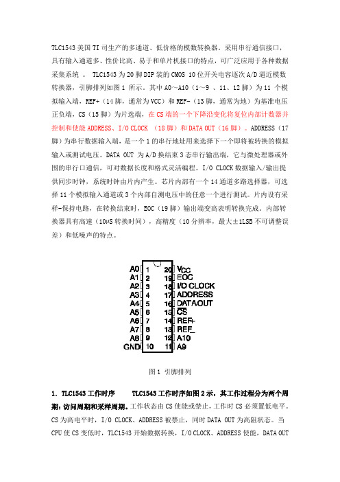
TLC1543为20脚DIP装的CMOS 10位开关电容逐次A/D逼近模数转换器,引脚排列如图1 所示。
其中A0~A10(1~9 、11、12脚)为11 个模拟输入端,REF+(14脚,通常为VCC)和REF-(13脚,通常为地)为基准电压正负端,CS(15脚)为片选端,在CS端的一个下降沿变化将复位内部计数器并控制和使能ADDRESS、I/O CLOCK (18脚)和DATA OUT(16脚)。
ADDRESS(17脚)为串行数据输入端,是一个1的串行地址用来选择下一个即将被转换的模拟输入或测试电压。
DATA OUT 为A/D换结束3态串行输出端,它与微处理器或外围的串行口通信,可对数据长度和格式灵活编程。
I/O CLOCK数据输入/输出提供同步时钟,系统时钟由片内产生。
芯片内部有一个14通道多路选择器,可选择11个模拟输入通道或3个内部自测电压中的任意一个进行测试。
片内设有采样-保持电路,在转换结束时,EOC(19脚)输出端变高表明转换完成。
内部转换器具有高速(10µS转换时间),高精度(10分辨率,最大±1LSB不可调整误差)和低噪声的特点。
图1 引脚排列1.TLC1543工作时序TLC1543工作时序如图2示,其工作过程分为两个周期:访问周期和采样周期。
工作状态由CS使能或禁止,工作时CS必须置低电平。
CS 为高电平时,I/O CLOCK、ADDRESS被禁止,同时DATA OUT为高阻状态。
当CPU 使CS变低时,TLC1543开始数据转换,I/O CLOCK、ADDRESS使能,DATA OUT脱离高阻状态。
随后,CPU向ADDRESS提供4位通道地址,控制14个模拟通道选择器从11个外部模拟输入和3个内部自测电压中选通1 路送到采样保持电路。
TLC1543
IMPORTANT NOTICETexas Instruments (TI) reserves the right to make changes to its products or to discontinue any semiconductor product or service without notice, and advises its customers to obtain the latest version of relevant information to verify, before placing orders, that the information being relied on is current.TI warrants performance of its semiconductor products and related software to the specifications applicable at the time of sale in accordance with TI’s standard warranty. Testing and other quality control techniques are utilized to the extent TI deems necessary to support this warranty. Specific testing of all parameters of each device is not necessarily performed, except those mandated by government requirements.Certain applications using semiconductor products may involve potential risks of death, personal injury, or severe property or environmental damage (“Critical Applications”).TI SEMICONDUCTOR PRODUCTS ARE NOT DESIGNED, INTENDED, AUTHORIZED, OR WARRANTED TO BE SUITABLE FOR USE IN LIFE-SUPPORT APPLICATIONS, DEVICES OR SYSTEMS OR OTHER CRITICAL APPLICATIONS.Inclusion of TI products in such applications is understood to be fully at the risk of the customer. Use of TI products in such applications requires the written approval of an appropriate TI officer. Questions concerning potential risk applications should be directed to TI through a local SC sales office.In order to minimize risks associated with the customer’s applications, adequate design and operating safeguards should be provided by the customer to minimize inherent or procedural hazards.TI assumes no liability for applications assistance, customer product design, software performance, or infringement of patents or services described herein. Nor does TI warrant or represent that any license, either express or implied, is granted under any patent right, copyright, mask work right, or other intellectual property right of TI covering or relating to any combination, machine, or process in which such semiconductor products or services might be or are used.Copyright © 1995, Texas Instruments Incorporated。
IBM 部分电源控制IC中文引脚说明

MAX1631的引脚说明PIN1:CSH3。
3.3V SMPS(开关电源Switch Mode Power Supply )电流检测输入,以CSL3为参考限流电平为100mV。
PIN2:CSL3。
电流检测输入。
常在固定输出模式里作为反馈输入。
PIN3:FB3。
3.3V SMPS的反馈输入;将FB3调整在REF(约2.5V)时为输出可调模式。
当FB3接地时,为固定3.3V输出。
当FB3连接一个分压电阻时为输出可调节模式。
PIN4:对MAX1630、MAX1632来说,此脚为12V输出。
可往外提供12V,120mA的电压。
但要外接一个1uF电容。
对MAX1631来说,此脚为STEER。
次级反馈的逻辑控制输入。
用来选择PWM采用那路变压器和次级反馈信号。
当STEER为GND时,SECFB(secondary feedback次级反馈采用3.3V 变压器次级反馈。
当STEER为VL时,SECFB采用5V 变压器次级反馈。
PIN5:对MAX1630、MAX1632,VDD。
内置线性12V的电源。
对MAX1631,SECFB,次级线圈反馈输入。
通常从辅助输出连接一个电阻分压器。
SECFB调整在。
当接时为不采用。
2.5V VLPIN6:SYNC,振荡同步和频率选择。
连接到VL时工作在300kHZ;接地工作在200kHZ。
当有外接同步时时钟范围可在240kHZ至350Khz。
PIN7:TIME/ON5,具有双用途,用作定时电容引脚和开关控制输入。
PIN8:GND,低噪音模拟地和反馈参考点。
PIN9:REF,2.5V参考电压输出。
接1uF电容至地。
PIN10:SKIP#。
逻辑控制输入。
当为高电平时取消空闲模式。
接地为正常模式。
PIN11:RESET#,低电平有效的定时复位输出。
RESET#在地至VL之间变化。
在上电后的32,000个周32000期变高电平。
PIN12:FB5,5V SMPS反馈输入;调整到FB5=REF(约2.5V)工作输出可调整模式。
MAXIM 化数字电位器MAX5481, MAX5482, MAX5483, MAX548 说明书

ENGLISH•简体中文•日本語•概述状况状况:生产中。
下载Notes MAX5481Linear13-WireSerial SPINon-Volatile102410253519.6$1.95@1kMAX548250$1.95 @1kMAX548310$1.95 @1kMAX548450$1.95 @1k查看所有Digital Potentiometers (128)引脚配置相关产品MAX5494,MAX5495,MAX5496, ...10位、双路、非易失、线性变化数字电位器类似产品:浏览其它类似产品线查看所有Digital Potentiometers (128产品)顶标MAX5481顶标MAX5482顶标MAX5483顶标MAX5484新品发布[ 2005-08-03 ]应用工程师帮助选型,下个工作日回复参数搜索应用帮助概述技术文档定购信息概述关键特性应用/使用关键指标图表注释、注解相关产品数据资料应用笔记评估板设计指南可靠性报告软件/模型价格与供货样品在线订购封装信息无铅信息参考文献: 19-3708 Rev. 4; 2008-03-12本页最后一次更新: 2008-03-27联络我们:信息反馈、提出问题 • 对该网页的评价 • 发送本网页 • 隐私权政策 • 法律声明 © 2010 Maxim Integrated Products版权所有General DescriptionThe MAX5481–MAX5484 10-bit (1024-tap) nonvolatile,linear-taper, programmable voltage-dividers and vari-able resistors perform the function of a mechanical potentiometer, but replace the mechanics with a pin-configurable 3-wire serial SPI™-compatible interface or up/down digital interface. The MAX5481/MAX5482 are 3-terminal voltage-dividers and the MAX5483/MAX5484are 2-terminal variable resistors.The MAX5481–MAX5484 feature an internal, non-volatile, electrically erasable programmable read-only memory (EEPROM) that stores the wiper position for ini-tialization during power-up. The 3-wire SPI-compatible serial interface allows communication at data rates up to 7MHz. A pin-selectable up/down digital interface is also available.The MAX5481–MAX5484 are ideal for applications requiring digitally controlled potentiometers. Two end-to-end resistance values are available (10k Ωand 50k Ω) in a voltage-divider or a variable-resistor configuration (see the Selector G uide ). The nominal resistor temperature coefficient is 35ppm/°C end-to-end, and only 5ppm/°C ratiometric, making these devices ideal for applications requiring low-temperature-coefficient voltage-dividers,such as low-drift, programmable gain-amplifiers.The MAX5481–MAX5484 operate with either a +2.7V to +5.25V single power supply or ±2.5V dual power sup-plies. These devices consume 400µA (max) of supply current when writing data to the nonvolatile memory and 1.0µA (max) of standby supply current. The MAX5481–MAX5484 are available in a space-saving (3mm x 3mm), 16-pin TQFN, or a 14-pin TSSOP pack-age and are specified over the extended (-40°C to +85°C) temperature range.ApplicationsFeatures♦1024 Tap Positions♦Power-On Recall of Wiper Position from Nonvolatile Memory♦16-Pin (3mm x 3mm x 0.8mm) TQFN or 14-Pin TSSOP Package♦35ppm/°C End-to-End Resistance Temperature Coefficient♦5ppm/°C Ratiometric Temperature Coefficient ♦10kΩand 50kΩEnd-to-End Resistor Values♦Pin-Selectable SPI-Compatible Serial Interface or Up/Down Digital Interface ♦1µA (max) Standby Current♦Single +2.7V to +5.25V Supply Operation ♦Dual ±2.5V Supply OperationMAX5481–MAX548410-Bit, Nonvolatile, Linear-Taper DigitalPotentiometers________________________________________________________________Maxim Integrated Products1Ordering InformationPin Configurations19-3708; Rev 5; 4/10For pricing delivery, and ordering information please contact Maxim Direct at 1-888-629-4642,or visit Maxim’s website at .Selector Guide appears at end of data sheet.SPI is a trademark of Motorola, Inc.temperature range.+Denotes a lead(Pb)-free/RoHS-compliant package.*EP = Exposed pad.Ordering Information continued at end of data sheet.Gain and Offset AdjustmentLCD Contrast Adjustment Pressure SensorsLow-Drift Programmable Gain AmplifiersMechanical Potentiometer ReplacementM A X 5481–M A X 548410-Bit, Nonvolatile, Linear-Taper Digital PotentiometersABSOLUTE MAXIMUM RATINGSStresses beyond those listed under “Absolute Maximum Ratings” may cause permanent damage to the device. These are stress ratings only, and functional operation of the device at these or any other conditions beyond those indicated in the operational sections of the specifications is not implied. Exposure to absolute maximum rating conditions for extended periods may affect device reliability.V DD to GND...........................................................-0.3V to +6.0V V SS to GND............................................................-3.5V to +0.3V V DD to V SS .............................................................-0.3V to +6.0V H, L, W to V SS ..................................(V SS - 0.3V) to (V DD + 0.3V)CS , SCLK(INC ), DIN(U/D ), SPI/UD to GND..-0.3V to (V DD + 0.3V)Maximum Continuous Current into H, L, and WMAX5481/MAX5483.........................................................±5mA MAX5482/MAX5484......................................................±1.0mA Maximum Current into Any Other Pin...............................±50mAContinuous Power Dissipation (T A = +70°C)16-Pin TQFN (derate 17.5mW/°C above +70°C).....1398.6mW 14-Pin TSSOP (derate 9.1mW/°C above +70°C)..........727mW Operating Temperature Range ...........................-40°C to +85°C Junction Temperature......................................................+150°C Storage Temperature Range.............................-60°C to +150°C Lead Temperature (soldering, 10s).................................+300°C Soldering Temperature (reflow).......................................+260°CELECTRICAL CHARACTERISTICSMAX5481–MAX548410-Bit, Nonvolatile, Linear-Taper DigitalPotentiometers_______________________________________________________________________________________3ELECTRICAL CHARACTERISTICS (continued)(V DD = +2.7V to +5.25V, V SS = V GND = 0V, V H = V DD , V L = 0V, T A = -40°C to +85°C, unless otherwise noted. Typical values are at V DD = +5.0V, T A = +25°C, unless otherwise noted.) (Note 1)M A X 5481–M A X 548410-Bit, Nonvolatile, Linear-Taper Digital Potentiometers 4_______________________________________________________________________________________TIMING CHARACTERISTICSNote 2:The DNL and INL are measured with the device configured as a voltage-divider with H = V DD and L = V SS . The wiper termi-nal (W) is unloaded and measured with a high-input-impedance voltmeter.Note 3:The DNL_R and INL_R are measured with D.N.C. unconnected and L = V SS = 0V. For V DD = +5V, the wiper terminal is dri-ven with a source current of I W = 80µA for the 50k Ωdevice and 400µA for the 10k Ωdevice. For V DD = +3V, the wiper termi-nal is driven with a source current of 40µA for the 50k Ωdevice and 200µA for the 10k Ωdevice.Note 4:The wiper resistance is measured using the source currents given in Note 3.Note 5:The device draws higher supply current when the digital inputs are driven with voltages between (V DD - 0.5V) and (V GND +0.5V). See Supply Current vs. Digital Input Voltage in the Typical Operating Characteristics .Note 6:Wiper settling test condition uses the voltage-divider configuration with a 10pF load on W. Transition code from 00000 00000to 01111 01111 and measure the time from CS going high to the wiper voltage settling to within 0.5% of its final value.MAX5481–MAX548410-Bit, Nonvolatile, Linear-Taper DigitalPotentiometers_______________________________________________________________________________________5-1.0-0.6-0.8-0.2-0.40.200.40.80.61.002563841285126407688961024DNL vs. CODE (MAX5483)CODED N L (L S B )V DD = 2.7V-1.0-0.6-0.8-0.2-0.40.200.40.80.61.002563841285126407688961024DNL vs. CODE (MAX5483)CODED N L (L S B )V DD = 5V-2.0-1.0-1.50-0.50.51.01.5 2.0INL vs. CODE (MAX5483)I N L (L S B )V DD = 2.7V02563841285126407688961024CODE-2.0-1.0-1.50-0.50.51.01.5 2.0INL vs. CODE (MAX5483)I N L (L S B )V DD = 3V2563841285126407688961024CODE-2.0-1.0-1.50-0.50.51.01.5 2.0INL vs. CODE (MAX5483)I N L (L S B )V DD = 5V02563841285126407688961024CODE-1.0-0.6-0.8-0.2-0.40.200.40.80.61.002563841285126407688961024DNL vs. CODE (MAX5481)CODED N L (L S B )-1.0-0.6-0.8-0.2-0.40.200.40.80.61.002563841285126407688961024DNL vs. CODE (MAX5481)CODED N L (L S B )V DD = 5V-1.0-0.6-0.8-0.2-0.40.200.40.80.61.002563841285126407688961024INL vs. CODE (MAX5481)CODEI N L (L S B )-1.0-0.6-0.8-0.2-0.40.200.40.80.61.002563841285126407688961024INL vs. CODE (MAX5481)CODEI N L (L S B )Typical Operating Characteristics(V DD = 5.0V, V SS = 0V, T A = +25°C, unless otherwise noted.)M A X 5481–M A X 548410-Bit, Nonvolatile, Linear-Taper Digital Potentiometers 6_______________________________________________________________________________________-1.0-0.6-0.8-0.2-0.40.200.40.80.61.002563841285126407688961024DNL vs. CODE (MAX5484)CODED N L (L S B )-1.0-0.6-0.8-0.2-0.40.200.40.80.61.002563841285126407688961024DNL vs. CODE (MAX5484)CODED N L (L S B )-1.0-0.6-0.8-0.2-0.40.200.40.80.61.002563841285126407688961024INL vs. CODE (MAX5484)CODEI N L (L S B )-1.0-0.6-0.8-0.2-0.40.200.40.80.61.002563841285126407688961024INL vs. CODE (MAX5484)CODEI N L (L S B )-1.0-0.6-0.8-0.2-0.40.200.40.80.61.002563841285126407688961024DNL vs. CODE (MAX5482)CODED N L (L S B )-1.0-0.6-0.8-0.2-0.40.200.40.80.61.002563841285126407688961024DNL vs. CODE (MAX5482)CODED N L (L S B )-1.0-0.6-0.8-0.2-0.40.200.40.80.61.002563841285126407688961024INL vs. CODE (MAX5482)CODEI N L (L S B )V DD = 2.7V-1.0-0.6-0.8-0.2-0.40.200.40.80.61.02563841285126407688961024INL vs. CODE (MAX5482)CODEI N L (L S B )V DD = 5V02010403050607080WIPER RESISTANCE vs. CODE (VARIABLE RESISTOR, T A = -40°C)M A X 5481 t o c 18R W (Ω)2563841285126407688961024CODETypical Operating Characteristics (continued)(V DD = 5.0V, V SS = 0V, T A = +25°C, unless otherwise noted.)MAX5481–MAX5484Typical Operating Characteristics (continued)(V DD = 5.0V, V SS = 0V, T A = +25°C, unless otherwise noted.)10-Bit, Nonvolatile, Linear-Taper DigitalPotentiometers_______________________________________________________________________________________702010403050607080WIPER RESISTANCE vs. CODE (VARIABLE RESISTOR, T A = +25°C)M A X 5481 t oc 19R W (Ω)2563841285126407688961024CODE2010403050607080WIPER RESISTANCE vs. CODE (VARIABLE RESISTOR, T A = +85°C)M A X 5481 t o c 20R W (Ω)2563841285126407688961024CODE10302050604070W-TO-L RESISTANCE vs. CODE(MAX5484)R W L (k Ω)02563841285126407688961024CODE02641012814W-TO-L RESISTANCE vs. CODE(MAX5483)R W L (k Ω)2563841285126407688961024CODE18.018.519.019.520.020.521.021.522.0012345WIPER RESISTANCE vs. WIPER VOLTAGE(VARIABLE RESISTOR)WIPER VOLTAGE (V)R W (Ω)-2.0-1.5-1.0-0.500.51.01.52.0-40-1510356085END-TO-END (R HL ) % CHANGE vs. TEMPERATURE (VOLTAGE-DIVIDER)M A X 5481 t o c 24TEMPERATURE (°C)E N D -T O -E N D R E S I S T A N C E C H A N G E (%)-2.0-1.5-1.0-0.500.51.01.52.0-40-1510356085WIPER-TO-END RESISTANCE (R WL ) % CHANGE vs. TEMPERATURE (VARIABLE RESISTOR)TEMPERATURE (°C)W I P E R -T O -E N D R E S I S T A N C E C H A N G E (%)00.30.90.61.21.5-4010-15356085STANDBY SUPPLY CURRENTvs. TEMPERATURETEMPERATURE (°C)I D D (μA )DIGITAL SUPPLY CURRENT vs. DIGITAL INPUT VOLTAGEDIGITAL INPUT VOLTAGE (V)I D D (μA )4.54.03.53.02.52.01.51.00.5110100100010,0000.15.0M A X 5481–M A X 548410-Bit, Nonvolatile, Linear-Taper Digital Potentiometers Typical Operating Characteristics (continued)(Circuit of Figure 1, T A = +25°C, unless otherwise noted.)1μs/divTAP-TO-TAP SWITCHING TRANSIENTRESPONSE (MAX5481)V W(AC-COUPLED)20mV/divCS 2V/divH = V DD , L = GND C W = 10pFFROM CODE 01 1111 1111TO CODE 10 0000 00004μs/divTAP-TO-TAP SWITCHING TRANSIENTRESPONSE (MAX5482)V W(AC-COUPLED)20mV/divCS 2V/divH = V DD , L = GND C W = 10pFFROM CODE 01 1111 1111TO CODE 10 0000 0000WIPER RESPONSE vs. FREQUENCY(MAX5481)FREQUENCY (kHz)G A I N (d B )100101-20-15-10-5-250.11000WIPER RESPONSE vs. FREQUENCY(MAX5482)FREQUENCY (kHz)G A I N (d B )100101-20-15-10-50-250.11000THD+N vs. FREQUENCY(MAX5481)FREQUENCY (kHz)T H D +N (%)1010.10.0010.010.11100.00010.01100THD+N vs. FREQUENCY(MAX5482)FREQUENCY (kHz)T H D +N (%)1010.10.0010.010.11100.00010.0110004020806012010014018016020002563841285126407688961024RATIOMETRIC TEMPERATURE COEFFICIENT vs. CODECODER A T I O M E T R I C T E M P C O (p p m )100300200500600400700VARIABLE-RESISTOR TEMPERATURECOEFFICIENT vs. CODET C V R (p p m )02563841285126407688961024CODE10-Bit, Nonvolatile, Linear-Taper DigitalPotentiometersPin DescriptionMAX5481–MAX5484M A X 5481–M A X 548410-Bit, Nonvolatile, Linear-Taper Digital Potentiometers Pin Description (continued)(MAX5483/MAX5484 Variable Resistors)MAX5481–MAX548410-Bit, Nonvolatile, Linear-Taper DigitalPotentiometersFunctional DiagramsM A X 5481–M A X 548410-Bit, Nonvolatile, Linear-Taper Digital Potentiometers Detailed DescriptionThe MAX5481/MAX5482 linear programmable voltage-dividers and the MAX5483/MAX5484 variable resistors feature 1024 tap points (10-bit resolution) (see the Functional Diagrams ). These devices consist of multi-ple strings of equal resistor segments with a wiper con-tact that moves among the 1024 points through a pin-selectable 3-wire SPI-compatible serial interface or up/down interface. The MAX5481/MAX5483 provide a total end-to-end resistance of 10k Ω, and the MAX5482/MAX5484 have an end-to-end resistance of 50k Ω. The MAX5481/MAX5482 allow access to the high, low, and wiper terminals for a standard voltage-divider configuration.MAX5481/MAX5482 ProgrammableVoltage-DividersThe MAX5481/MAX5482 programmable voltage-dividers provide a weighted average of the voltage between the H and L inputs at the W output. Both devices feature 10-bit resolution and provide up to 1024 tap points between the H and L voltages. Ideally,the V L voltage occurs at the wiper terminal (W) when all data bits are zero and the V H voltage occurs at the wiper terminal when all data bits are one. The step size (1 LSB) voltage is equal to the voltage applied across terminals H and L divided by 210. Calculate the wiper voltage V Was follows:Functional Diagrams (continued)MAX5481–MAX548410-Bit, Nonvolatile, Linear-Taper DigitalPotentiometerswhere D is the decimal equivalent of the 10 data bits writ-ten (0 to 1023), V HL is the voltage difference between the H and L terminals:The MAX5481 includes a total end-to-end resistance value of 10k Ωwhile the MAX5482 features an end-to-end resistance value of 50k Ω. These devices are not intended to be used as a variable resistor . Wiper cur-rent creates a nonlinear voltage drop in series with the wiper. To ensure temperature drift remains within speci-fications, do not pull current through the voltage-divider wiper. Connect the wiper to a high-impedance node.Figures 1 and 2 show the behavior of the MAX5481’s resistance from W to H and from W to L. This does not apply to the variable-resistor devicesMAX5483/MAX5484 Variable ResistorsThe MAX5483/MAX5484 provide a programmable resistance between W and L. The MAX5483 features a total end-to-end resistance value of 10k Ω, while the MAX5484 provides an end-to-end resistance value of 50k Ω. The programmable resolution of this resistance is equal to the nominal end-to-end resistance divided by 1024 (10-bit resolution). For example, each nominal segment resistance is 9.8Ωand 48.8Ωfor the MAX5483and the MAX5484, respectively.wiper position from the 1024 possible positions, result-ing in 1024 values for the resistance from W to L.Calculate the resistance from W to L (R WL ) by using the where D is decimal equivalent of the 10 data bits writ-ten, R W-L is the nominal end-to-end resistance, and R Z is the zero-scale error. Table 1 shows the values of R WL at selected codes for the MAX5483/MAX5484.Digital InterfaceConfigure the MAX5481–MAX5484 by a pin-selectable,3-wire, SPI-compatible serial data interface or an up/down interface. Drive SPI/UD high to select the 3-wire SPI-compatible interface. Pull SPI/UD low to select the up/down interface.V FSE V andV ZSE V FSE HL ZSE HL =⎡⎣⎢⎤⎦⎥=⎡⎣⎢⎤⎦⎥10241024,Figure 1. Resistance from W to H vs. Code (10k ΩVoltage-Divider)Figure 2. Resistance from W to L vs. Code (10k ΩVoltage-Divider)M A X 5481–M A X 548410-Bit, Nonvolatile, Linear-Taper Digital Potentiometers SPI-Compatible Serial InterfaceDrive SPI/UD high to enable the 3-wire SPI-compatible serial interface (see Figure 3). This write-only interface contains three inputs: chip select (CS ), data in (DIN(U/D )), and data clock (SCLK(INC )). Drive CS low to load the data at DIN(U/D ) synchronously into the shift register on each SCLK(INC ) rising edge.The WRITE command (C1, C0 = 00) requires 24 clock cycles to transfer the command and data (Figure 4a).The COPY commands (C1, C0 = 10 or 11) use either eight clock cycles to transfer the command bits (Figure 4b) or 24 clock cycles with the last 16 data bits disre-garded by the device.After loading the data into the shift register, drive CS high to latch the data into the appropriate control regis-ter. Keep CS low during the entire serial data stream to avoid corruption of the data. Table 2 shows the com-mand decoding.Write Wiper RegisterData written to this register (C1, C0 = 00) controls the wiper position. The 10 data bits (D9–D0) indicate the position of the wiper. For example, if DIN(U/D ) = 00 00000000, the wiper moves to the position closest to L. If DIN(U/D ) = 11 1111 1111, the wiper moves closest to H.This command writes data to the volatile random access memory (RAM), leaving the NV register unchanged. When the device powers up, the data stored in the NV register transfers to the wiper register,moving the wiper to the stored position. Figure 5 shows how to write data to the wiper register.Table 2. Command Decoding*X = Don’t care.Figure 3. SPI-Compatible Serial-Interface Timing Diagram (SPI/UD = 1)10-Bit, Nonvolatile, Linear-Taper DigitalPotentiometers ArrayMAX5481–MAX5484Figure4. Serial SPI-Compatible Interface FormatFigure5. Write Wiper Register OperationM A X 5481–M A X 548410-Bit, Nonvolatile, Linear-Taper Digital Potentiometers Copy Wiper Register to NV RegisterThe copy wiper register to NV register command (C1,C0 = 10) stores the current position of the wiper to the NV register for use at power-up. Figure 6 shows how to copy data from wiper register to NV register. The oper-ation takes up to 12ms (max) after CS goes high to complete and no other operation should be performed until completion.Copy NV Register to Wiper RegisterThe copy NV register to wiper register (C1, C0 = 11)restores the wiper position to the current value stored in the NV register. Figure 7 shows how to copy data from the NV register to the wiper register.Digital Up/Down InterfaceFigure 8 illustrates an up/down serial-interface timing diagram. In digital up/down interface mode (SPI/UD =0), the logic inputs CS , DIN(U/D ), and SCLK(INC ) con-trol the wiper position and store it in nonvolatile memory (see Table 3). The chip-select (CS ) input enables the serial interface when low and disables the interface when high. The position of the wiper is stored in the nonvolatile register when CS transitions from low to high while SCLK(INC ) is high.When the serial interface is active (CS low), a high-to-low (falling edge) transition on SCLK(INC ) increments or decrements the internal 10-bit counter depending on the state of DIN(U/D ). If DIN(U/D ) is high, the wiper increments. If DIN(U/D ) is low, the wiper decrements.The device stores the value of the wiper position in the nonvolatile memory when CS transitions from low to high while SCLK(INC ) is high. The host system can disablethe serial interface and deselect the device without stor-ing the latest wiper position in the nonvolatile memory by keeping SCLK(INC ) low while taking CS high.Upon power-up, the MAX5481–MAX5484 load the value of nonvolatile memory into the wiper register, and set the wiper position to the value last stored.Figure 6. Copy Wiper Register to NV Register OperationFigure 7. Copy NV Register to Wiper Register OperationMAX5481–MAX548410-Bit, Nonvolatile, Linear-Taper DigitalPotentiometersStandby ModeThe MAX5481–MAX5484 feature a low-power standby mode. When the device is not being programmed, it enters into standby mode and supply current drops to 0.5µA (typ).Nonvolatile MemoryThe internal EEPROM consists of a nonvolatile register that retains the last value stored prior to power-down.The nonvolatile register is programmed to midscale at the factory. The nonvolatile memory is guaranteed for 50 years of wiper data retention and up to 200,000wiper write cycles.Power-UpUpon power-up, the MAX5481–MAX5484 load the data stored in the nonvolatile wiper register into the volatile wiper register, updating the wiper position with the data stored in the nonvolatile wiper register.Applications InformationThe MAX5481–MAX5484 are ideal for circuits requiring digitally controlled adjustable resistance, such as LCD contrast control (where voltage biasing adjusts the dis-play contrast), or programmable filters with adjustable gain and/or cutoff frequency.Positive LCD Bias ControlFigures 9 and 10 show an application where a voltage-divider or a variable resistor is used to make an adjustable, positive LCD-bias voltage. The op amp pro-vides buffering and gain to the voltage-divider network made by the programmable voltage-divider (Figure 9) or to a fixed resistor and a variable resistor (see Figure 10).Programmable Gain and Offset AdjustmentFigure 11 shows an application where a voltage-divider and a variable resistor are used to make a programma-ble gain and offset adjustment.Figure 8. Up/Down Serial-Interface Timing Diagram (SPI/UD = 0)M A X 5481–M A X 548410-Bit, Nonvolatile, Linear-Taper Digital Potentiometers 18______________________________________________________________________________________Programmable FilterFigure 12 shows the configuration for a 1st-order pro-grammable filter using two variable resistors. Adjust R2for the gain and adjust R3 for the cutoff frequency. Use the following equations to estimate the gain (G) and the 3dB cutoff frequency (f C):Figure 10. Positive LCD Bias Control Using a Variable ResistorFigure 12. Programmable FilterFigure 11. Programmable Gain/Offset AdjustmentFigure 9. Positive LCD Bias Control Using a Voltage-DividerMAX5481–MAX548410-Bit, Nonvolatile, Linear-Taper DigitalPotentiometers______________________________________________________________________________________19Chip InformationPROCESS: BiCMOSSelector GuidePin Configurations (continued)Ordering Information (continued)Note: All devices are specified over the -40°C to +85°C operating temperature range.+Denotes a lead(Pb)-free/RoHS-compliant package.*EP = Exposed pad.Package InformationFor the latest package outline information and land patterns, go to /packages . Note that a “+”, “#”, or “-” in the package code indicates RoHS status only. Package draw-ings may show a different suffix character, but the drawing per-tains to the package regardless of RoHS status.M A X 5481–M A X 548410-Bit, Nonvolatile, Linear-Taper Digital Potentiometers Maxim cannot assume responsibility for use of any circuitry other than circuitry entirely embodied in a Maxim product. No circuit patent licenses are implied. Maxim reserves the right to change the circuitry and specifications without notice at any time.20____________________Maxim Integrated Products, 120 San Gabriel Drive, Sunnyvale, CA 94086 408-737-7600©2010 Maxim Integrated ProductsMaxim is a registered trademark of Maxim Integrated Products, Inc.。
MAX320-MAX322中文资料
ELECTRICAL CHARACTERISTICS
(V+ = +5V ±10%, V- = -5V ±10%, VINH = 3.5V, VINL = 2.5V, TA = TMIN to TMAX, unless otherwise noted.)
PARAMETER ANALOG SWITCH Analog Signal Range
For equivalent devices specified for single-supply operation, see the MAX323/MAX324/MAX325 data sheet. For quad versions of these switches, see the MAX391/MAX392/MAX393 data sheet.
Plastic DIP (derate 9.09mW/°C above +70°C) .............727mW Narrow SO (derate 5.88mW/°C above +70°C) .............471mW
µMAX (derate 4.10mW/°C above +70°C) .....................330mW CERDIP (derate 8.00mW/°C above +70°C) ..................640mW Operating Temperature Ranges MAX32_C_ _ ........................................................0°C to +70°C MAX32_E_ _......................................................-40°C to +85°C MAX32_MJA ...................................................-55°C to +125°C Storage Temperature Range .............................-65°C to +150°C Lead Temperature (soldering, 10sec) .............................+300°C
MAX1483ESA+中文资料

元器件交易网
µMAX is a registered trademark of Maxim Integrated products, Inc.
________________________________________________________________ Maxim Integrated Products 1
元器件交易网
19-0367; Rev 1; 5/06
MAX1482/MAX1483
20µA, 1⁄8-Unit-Load, Slew-Rate-Limited RS-485 Transceivers
_______________General Description
The MAX1482 and MAX1483 are low-power transceivers for RS-485 and RS-422 communication. Both feature slew-rate-limited drivers that minimize EMI and reduce reflections caused by improperly terminated cables. Data rates are guaranteed up to 250kbps. The MAX1482/MAX1483 draw only 20µA of supply current. Additionally, they have a low-current shutdown mode that consumes only 0.1µA. Both parts operate from a single +5V supply. Drivers are short-circuit current limited and are protected against excessive power dissipation by thermal shutdown circuitry that places the driver outputs into a high-impedance state. The receiver input has a fail-safe feature that guarantees a logic-high output if the input is open circuit. The MAX1482 is full duplex and the MAX1483 is half duplex. Both parts have a 1⁄8-unit-load input impedance that guarantees up to 256 transceivers on the bus.
TDA1543中文资料

元器件交易网
Philips Semiconductors
Dual 16-bit DAC (economy version) (I2S input format)
Product specification
TDA1543
PINNING
SYMBOL PIN
DESCRIPTION
This flexible input data format (I2S) allows easy interfacing with signal processing chips such as interpolation filters, error correction circuits and audio signal processor circuits (ASP).
ORDERING INFORMATION
EXTENDED TYPE NUMBER
TDA1543(1)
8
TDA1543T(2)
16
PINS
Notes 1. SOT97-1; 1996 August 13. 2. SOT162-1 1996 August 13.
PIN POSITION DIL mini-pack
13 reference voltage output 14 right channel output
n.c.
15 not connected
n.c.
16 not connected
handbook, halfpage
n.c. n.c.
BCK 3
14 AOR
WS 4
supply voltage
supply current
full scale output current
智能仪器3

(2)MC14433MC14433是Motorola公司的3(1/2)位双积分型A/D转换器。
分辨率相当于二进制11位,远高于ADC0809,转换时间100m S,转换误差小于±1LSB。
具有自动调零、自动极性判断功能,具有自动量程控制信号输出,数据输出采用动态字位扫描BCD码输出。
曾经广泛应用于各类模拟量测量仪器。
1)引脚功能简介:见附图3-3所示。
2)时钟频率f CP的选择:如果正向积分阶段的时间(4000*T CP)是干扰信号周期的整倍数,对此干扰抑制效果很好,如50Hz工频干扰的周期为20mS,取正向积分时间为40mS,则40000μS=4000×T CP,即T CP=40000μS/4000=10μS,f CP=1/T CP=1/10μS=100kHz。
其关系请参见《中国集成电路大全—CMOS集成电路》P600图13-76所示,当R C=300kΩ时f CP≈100kHz。
3)A/D转换速度:A/D转换速度由f CP决定。
该芯片完成1次A/D转换需要16400个时钟周期,当f CP=100kHz即T CP=10μS时,转换周期为T≈16400*10μS=164mS,A/D转换速度约每秒6次。
为提高对50Hz工频干扰的抗干扰能力,正向积分时间应≥20mS,即T CP≥20000μS/4000=5μS,转换周期为T≥16400*5μS=82mS/次,所以,转换速度应≤12.2次/s。
若不考虑抗干扰性能,该芯片的最高转换速度可达30次/秒。
4)千位编码:Q3—千位值,千位数转换结果为1时,输出低电平,Q3=0。
Q2—电压极性,正极性时输出高电平,Q2=1。
Q0—超量程范围标志,Q0=1表示超量程范围,若同时Q3=0表示过量程;若同时Q3=1表示欠量程。
5) 输出时序:见附图3-4所示。
6) 接口电路设计:MC14433的Q0~Q3、DS1~DS4连接到AT89C51的P1.0~P1.7;MC14433的EOC (A/D 转换结束标志)与DU (更新A/D 转换结果)相连后,实现连续转换,再连接到AT89C51的INT0作为中断请求信号,见附图3-5所示。
- 1、下载文档前请自行甄别文档内容的完整性,平台不提供额外的编辑、内容补充、找答案等附加服务。
- 2、"仅部分预览"的文档,不可在线预览部分如存在完整性等问题,可反馈申请退款(可完整预览的文档不适用该条件!)。
- 3、如文档侵犯您的权益,请联系客服反馈,我们会尽快为您处理(人工客服工作时间:9:00-18:30)。
ELECTRICAL CHARACTERISTICS
(VIN = 3V, VSUP = 8V, VSRC = 28V, FREQ = IN (MAX1543), PGND = AGND = 0, TA = 0°C to +85°C, typical values at TA = +25°C, unless otherwise noted.)
o Ultra-High-Performance Step-Up Regulator Fast Transient Response to Pulsed Load Using Current-Mode Control Architecture High-Accuracy Output Voltage (1.3%) Built-In 14V, 1.2A, 0.2Ω N-Channel Power MOSFET with Lossless Current-Sensing High Efficiency (85%) 8-Step Current-Controlled Digital Soft-Start o Two High-Performance Operational Amplifiers 150mA Output Short-Circuit Current 7.5V/µs Slew Rate 12MHz -3dB Bandwidth Rail-to-Rail Inputs/Outputs Unity Gain Stable o Logic-Controlled High-Voltage Switch with Adjustable Delay o Timer Delay Latch FB Fault Protection o Thermal Protection o 2.6V to 5.5V Input Operating Voltage Range o 3.6mA (Switching), 0.45mA (Not Switching) Quiescent Current o Ultra-Thin 20-Pin Thin QFN Package (5mm x 5mm x 0.8mm)
NEG1
OUT2
9
Rail-to-Rail is a registered trademark of Nippon Motorola, Ltd. 1
________________________________________________________________ Maxim Integrated Products
TOP VIEW
20
19
18
17
COMP
COM SRC I.C. PGND AGND
1 2 3 4 5 NEG2 10
16
15 14
FREQ IN LX SUP POS2
MAX1543
13 12 11
6
7
8பைடு நூலகம்
OUT1
POS1
THIN QFN (5mm x 5mm)
Pin Configurations continued at end of data sheet.
MAX1542/MAX1543
The MAX1542/MAX1543 include a high-performance boost regulator and two high-current operational amplifiers for active matrix, thin-film transistor (TFT), liquidcrystal displays (LCDs). Also included is a logiccontrolled, high-voltage switch with adjustable delay. The MAX1543 includes an additional high-voltage load switch and features pin-selectable boost regulator switching frequency. The step-up DC-to-DC converter is a high-frequency 640kHz (MAX1543)/1.2MHz (MAX1542/MAX1543) current-mode regulator with a built-in power MOSFET that allows the use of ultra-small inductors and ceramic capacitors. It provides fast transient response to pulsed loads while producing efficiencies over 85%. The two easy-to-use, high-performance operational amplifiers can drive the LCD backplane (VCOM) and/or the gamma correction divider string. The devices feature high short-circuit current (150mA), fast slew rate (7.5V/µs), wide bandwidth (12MHz), and Rail-to-Rail® inputs and outputs. The MAX1542/MAX1543 are available in 20-pin thin QFN packages with a maximum thickness of 0.8mm for ultra-thin LCD panel design.
For pricing, delivery, and ordering information, please contact Maxim/Dallas Direct! at 1-888-629-4642, or visit Maxim’s website at .
元器件交易网
元器件交易网
19-2741; Rev 0; 4/03
KIT ATION EVALU LE B A IL A AV
TFT LCD DC-to-DC Converter with Operational Amplifiers
General Description Features
Stresses beyond those listed under “Absolute Maximum Ratings” may cause permanent damage to the device. These are stress ratings only, and functional operation of the device at these or any other conditions beyond those indicated in the operational sections of the specifications is not implied. Exposure to absolute maximum rating conditions for extended periods may affect device reliability.
TFT LCD DC-to-DC Converter with Operational Amplifiers MAX1542/MAX1543
ABSOLUTE MAXIMUM RATINGS
IN, CTL, COMP, FB, DEL, FREQ (MAX1543) to AGND ...............................................................-0.3V to +6V COMP, FB, DEL to AGND .............................-0.3V to (IN + 0.3V) PGND to AGND ..................................................................±0.3V LX to PGND ............................................................-0.3V to +14V SUP, POS1, NEG1, OUT1, POS2, NEG2, OUT2 to AGND .......................................-0.3V to +14V POS1, NEG1, OUT1, POS2, NEG2, OUT2 to AGND ......................................-0.3V to (SUP + 0.3V) SRC, COM to AGND...............................................-0.3V to +30V SRC to COM ...........................................................-0.3V to +30V SRC to DRN (MAX1543).........................................-0.3V to +30V COM to AGND ...........................................-0.3V to (SRC + 0.3V) DRN (MAX1543) to AGND .........................-0.3V to (SRC + 0.3V) DRN (MAX1543) to COM.........................................-30V to +30V MAX1542 COM RMS Output Current ...............................+75mA MAX1543 COM RMS Output Current ...............................±50mA OUT1, OUT2 Continuous Output Current.........................±75mA Continuous Power Dissipation (TA = +70°C) 20-Pin Thin QFN 5mm x 5mm (derate 20.8mW/°C above +70°C) .............................1667mW Operating Temperature Range ...........................-40°C to +85°C Junction Temperature .....................................................+150°C Storage Temperature Range .............................-65°C to +150°C Lead Temperature (soldering, 10s) .................................+300°C