YNC9.6S20A-0中文资料
2SA966资料

TOSHIBA Transistor Silicon PNP Epitaxial Type (PCT Process)2SA966Audio Power Amplifier Applications• Complementary to 2SC2236 and 3-W output applications.Absolute Maximum Ratings (Ta = 25°C)Characteristics Symbol Rating UnitCollector-base voltage V CBO −30 V Collector-emitter voltage V CEO −30 V Emitter-base voltage V EBO −5 V Collector current I C−1.5 AEmitter currentI E 1.5 A Collector power dissipation P C 900 mW Junction temperature T j 150 °C Storage temperature rangeT stg−55 to 150°CNote: Using continuously under heavy loads (e.g. the application of high temperature/current/voltage and the significant change in temperature, etc.) may cause this product to decrease in thereliability significantly even if the operating conditions (i.e. operating temperature/current/voltage, etc.) are within the absolute maximum ratings.Please design the appropriate reliability upon reviewing the Toshiba Semiconductor Reliability Handbook (“HandlingPrecautions”/Derating Concept and Methods) and individual reliability data (i.e. reliability test report and estimated failure rate, etc).Unit: mmJEDEC TO-92MOD JEITA ―TOSHIBA 2-5J1A Weight: 0.36 g (typ.)Electrical Characteristics (Ta = 25°C)Characteristics Symbol TestCondition MinTyp.Max UnitCollector cut-off current I CBO V CB = −30 V, I E = 0 ――−100nAEmitter cut-off current I EBO V EB = −5 V, I C = 0 ――−100nA Collector-emitter breakdown voltage V (BR) CEO I C = −10 mA, I B = 0 −30 ―― V Emitter-base breakdown voltage V (BR) EBO I E = −1 mA, I C = 0 −5 ―― VDC current gain h FE(Note)V CE = −2 V, I C = −500 mA 100 ― 320Collector-emitter saturation voltage V CE (sat)I C = −1.5 A, I B = −0.03 A ――−2.0V Base-emitter voltage V BE V CE = −2 V, I C = −500 mA ――−1.0V Transition frequency f T V CE = −2 V, I C = −500 mA ― 120 ― MHz Collector output capacitance C ob V CB = −10 V, I E = 0, f = 1 MHz ― 40 ― pF Note: h FE classification O: 100 to 200, Y: 160 to 320Markinglead (Pb)-free package orlead (Pb)-free finish.indicatorCollector current I C (mA)h FE – ICD C c u r re n t g a i n h F ECollector current I C (mA)V CE (sat) – I CC o l l e c t o r -e m i t t e r s a t u r a t i on v o l t a g eV C E (s a t ) (V )Base-emitter voltage V BE (V)I C – V BEC oll e c t o rc u r r e n t I C (m A )Ambient temperature Ta (°C)P C – TaC o l l e c t o r p owe r d i s s ip a t io n P C (W )Collector-emitter voltage V CE (V)Safe Operating AreaC o l l e c t o r c u r r e n t I C (A )1.00 0 20 40 60 80 100 120 140 160 1800.20.40.60.8−−−−−−−−−−−−−−−−−−Collector-emitter voltage V CE (V)I C – V CEC o l l e c t o r c u r r e n t I C (m A )−−−−−−−−−−−−−−−−−RESTRICTIONS ON PRODUCT USE20070701-EN •The information contained herein is subject to change without notice.•TOSHIBA is continually working to improve the quality and reliability of its products. Nevertheless, semiconductor devices in general can malfunction or fail due to their inherent electrical sensitivity and vulnerability to physical stress. It is the responsibility of the buyer, when utilizing TOSHIBA products, to comply with the standards of safety in making a safe design for the entire system, and to avoid situations in which a malfunction or failure of such TOSHIBA products could cause loss of human life, bodily injury or damage to property.In developing your designs, please ensure that TOSHIBA products are used within specified operating ranges as set forth in the most recent TOSHIBA products specifications. Also, please keep in mind the precautions and conditions set forth in the “Handling Guide for Semiconductor Devices,” or “TOSHIBA Semiconductor Reliability Handbook” etc.• The TOSHIBA products listed in this document are intended for usage in general electronics applications (computer, personal equipment, office equipment, measuring equipment, industrial robotics, domestic appliances, etc.).These TOSHIBA products are neither intended nor warranted for usage in equipment that requires extraordinarily high quality and/or reliability or a malfunction or failure of which may cause loss of human life or bodily injury (“Unintended Usage”). Unintended Usage include atomic energy control instruments, airplane or spaceship instruments, transportation instruments, traffic signal instruments, combustion control instruments, medical instruments, all types of safety devices, etc.. Unintended Usage of TOSHIBA products listed in his document shall be made at the customer’s own risk.•The products described in this document shall not be used or embedded to any downstream products of which manufacture, use and/or sale are prohibited under any applicable laws and regulations.• The information contained herein is presented only as a guide for the applications of our products. No responsibility is assumed by TOSHIBA for any infringements of patents or other rights of the third parties which may result from its use. No license is granted by implication or otherwise under any patents or other rights of TOSHIBA or the third parties.• Please contact your sales representative for product-by-product details in this document regarding RoHS compatibility. Please use these products in this document in compliance with all applicable laws and regulations that regulate the inclusion or use of controlled substances. Toshiba assumes no liability for damage or losses occurring as a result of noncompliance with applicable laws and regulations.。
2N3906三极管规格书
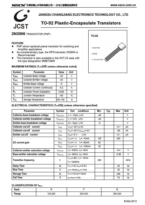
JIANGSU CHANGJIANG ELECTRONICS TECHNOLOGY CO., LTD
TO-92 Plastic-Encapsulate Transistors
2N3906 TRANSISTOR (PNP)
-100 -80 -60 -40 -20 -0 -0
-1000
-300 -100
-30
Static Characteristic
-500uA -450uA -400uA -350uA
-300uA
-250uA
COMMON
EMITTER T =25℃
a
-200uA
-150uA
-100uA
I =-50uA
C / C —— V / V
ob ib
CB EB
β=10
-100
-200
f=1MHz
I =0/I =0
E
C
T =25℃ a
Cib Cob
1 -0.1
750 625 500 375 250 125
0 0
-0.3
-1
-3
-10
-20
REVERSE BIAS VOLTAGE V (V)
P —— T
C
a
25
DC current gain
Collector-emitter saturation voltage Base-emitter saturation voltage
Transition frequency
Delay Time Rise Time Storage Time Fall Time
Symbol V(BR)CBO V(BR)CEO V(BR)EBO
轴承代号含义说明之欧阳术创编
轴承代号含义说明轴承代号由基本代号,前置代号和后置代号构成。
基本代号表示轴承系列及尺寸,前置代号表示轴承类型及轴承零件,位于基本代号之前,后置代号表示轴承的结构,保持架,密封与防尘,公差,油隙,热处理等技术要求,位于基本代号之后。
1.前置代号C- 圆柱滚子轴承附件(或轴承本身),例:C00210 45C- 成对安装圆锥滚子轴承,面对面安装,例:45C30210 46C- 成对安装圆锥滚子轴承,背对背安装,例:46C30210 4CRI- 四列圆柱滚子轴承内圈,例:4CRI4560F 4CRO- 四列圆柱滚子轴承外圈,例:4CRO660AF E- 磁电机球轴承,外径为正公差,例:E10 EN- 磁电机球轴承,外径为负公差,例:EN10 IR- 滚针轴承内圈(英制),例:IR1212 IRA- 滚针轴承内圈,比IR系列宽(英制),例:IRA20 IRM- 滚针轴承内圈,例:IRM710 M- 最大载荷容量型球轴承,例:M6311 OR- 滚针轴承,只有外圈,例:OR10876 F- 深沟球轴承带凸缘,例:F603TR- 尺寸非标准的单列圆锥滚子轴承,例:TR060702 W- 宽型,深沟球轴承,例:W602ZZX2.后置代号(1)内部结构A- 角接触轴承,接触角30度(不标出),例:7210 B- 角接触轴承,接触角40度,例:7210B C- 角接触轴承,接触角15度,例:7210C C- 圆锥滚子轴承,接触角20度,例:30303C D- 圆锥滚子轴承,接触角28度30分,例:30305D G- 压缩轴向油隙的调心和圆锥滚子轴承J- 圆锥滚子轴承,符合ISO分组,例:30206J N- 圆锥滚子轴承,特殊噪声要求,例:30208N R- 加大负荷容量的调心,圆锥和圆柱滚子轴承,例:22228R (2)密封和防尘OR- 球轴承带O型密封圈,例:6201+OR RK- 单面,双唇接触式合成橡胶密封,例:6210RK 2RK- 双面,双唇接触式合成橡胶密封,例:6210.2RK RS- 单面,接触式合成橡胶密封,例:6210RS 2RS- 双面,接触式合成橡胶密封,例:6210-2RS RSA- 单面,带金属罩接触式合成橡胶密封,例:88107RSA 2RSA- 双面,带金属罩接触式合成橡胶密封,例:88107-2RSA RSB- 单面,带加卡金属罩的接触式合成橡胶密封,例:88107RSB2RSB- 双面,带加卡金属罩的接触式合成橡胶密封,例:88107-2RSBRSC- 硅橡胶制RS型密封,例:6210RSCRSD- 聚丙烯橡胶制RS型密封,例:6210RSD RSE- 单面,挡边引导接触式合成橡胶密封,例:6206RSE 2RSE- 双面,挡边引导接触式合成橡胶密封,例:6206-2RSE RSF- RS型氟化橡胶密封,例:6210RSF RU- 单面,非接触式合成橡胶密封,例:6205RU 2RU- 双面,非接触式合成橡胶密封,例:6205-2RU TR- 单面,三唇金属罩合成橡胶密封,例:4508B-TR 2TR- 双面,三唇金属罩合成橡胶密封,例:4508B-2TR U- 一面带接触式合成橡胶密封的滚针轴承,例:NA4916U UU- 二面带接触式合成橡胶密封的滚针轴承,例:NA4916UU Z- 单面钢制防尘盖,例:6205.Z ZZ- 双面钢制防尘盖,例:6205ZZ ZL- 单面,L型内径的钢制防尘盖,例:6207ZL ZX- 单面,由止动环压紧的钢制防尘盖,例:6205ZX ZXL- 由止动环压紧L型内径单面钢制防尘盖,例:6203ZXL ZZL- 钢制防尘盖,双面,L型内径,例:6203ZZL ZZX- 钢制防尘盖,双面,由止动环压紧,例:605ZZX ZZXL- 钢制防尘盖,双面,由止动环压紧,L型内径,例:6303ZZXL(3)套圈形状a- 大于标准倒角的非标准倒角,例:6205a B- 圆锥滚子轴承,外圈带凸缘,例:30210B BI- 双半内圈球轴承,例:6215BI BO- 双半外圈球轴承,例:6215BO D- 圆锥滚子轴承,双外圈或双内圈(英制),例:594/592D K- 带锥孔轴承,锥度为1:12,例:1210K K30- 带锥孔轴承,锥度为1:30,例:23026K30 N- 外圈带止动槽轴承,例:6206N C- 带锁孔的圆锥滚子轴承NR- 外圈带止动环轴承,例:6210NR Y- 小于标准倒角尺寸的非标准倒角,例:30206Y S- 圆锥滚子轴承,非标准倒角(斜倒角)SG- 内径带螺旋槽的圆锥滚子轴承T- 锥孔或锥形外径(英制)圆锥滚子轴承TD- 双列、锥孔或锥形外径(英制)圆锥滚子轴承W- 双内圈、端面带槽的圆锥滚子轴承,例:47T694625WH W- 外圈有润滑油沟槽和孔的圆柱滚子轴承,例:NU316W Wi- 圆柱滚子轴承(1-外圈有润滑油孔;2-内圈有润滑油孔和槽;3-内圈有润滑油孔;4-内、外圈有润滑油孔;5-内、外圈有润滑油孔和槽;6-外圈有润滑油孔和槽,内圈有润滑油孔;10-外圈带锁孔;11-外圈带润滑油孔和锁孔;13-外圈带锁孔,内圈带润滑油孔;14-内圈带润滑油孔,外圈带润滑油孔和锁孔;I=1,2,…)。
2N3906中文资料(nte)中文数据手册「EasyDatasheet - 矽搜」
VCE = 1V, I C = 1mA
40 − − 80 − −
2N3905 2N3906
VCE = 1V, I C = 10mA
50 − 150 100 − 300
2N3905 2N3906
VCE = 1V, I C = 50mA
30 − − 60 − −
2N3905 2N3906
VCE = 1V, I C = 100mA
芯片中文手册,看全文,戳
2N3905 & 2N3906 硅PNP晶体管
一般用途
TO92类型封装
绝对最大额定值:
集电极 - 发射极电压,V
CEO . . . . . . . . . . . . . . . . . . . . . . . . . . . . . . . . . . . . . . . . . . . . . . . . . . . . . . 40V
器件总功耗(T
C = +255C), PD . . . . . . . . . . . . . . . . . . . . . . . . . . . . . . . . . . . . . . . . . . . . 1.5W
减免上述255℃. . . . . . . . . . . . . . . . . . . . . . . . . . . . . . . . . . . . . . . . . . . . . . . . . . . . . . 12MW / 5C
减免上述255℃. . . . . . . . . . . . . . . . . . . . . . . . . . . . . . . . . . . . . . . 5.0MW / 5C
器件总功耗(T
集成电路型号功能对照表20页word文档

集成电路型号功能对照表0206A 天线开关集成电路03VFG9 发射压控振荡集成电路1021AC 发射压控振荡集成电路1097C 升压集成电路140N 电源取样比较放大集成电路14DN363 伺服控制集成电路15105 充电控制集成电路15551 管理卡升压集成电路1710 视频信号处理集成电路1N706 混响延时集成电路20810-F6096 存储集成电路2252B 微处理集成电路2274 延迟集成电路24C01ACEA 存储集成电路24C026 存储集成电路24C04 存储集成电路24C64 码片集成电路24LC16B 存储集成电路24LC65 电可改写编程只读存储集成电路27C1000PC-12 存储集成电路27C2000QC-90 存储集成电路27C20T 存储集成电路27C512 电可改写编程只读存储集成电路2800 红外遥控信号接收集成电路28BV64 码片集成电路28F004 版本集成电路31085 射频电源集成电路32D54 电源、音频信号处理集成电路32D75 电源、音频信号处理集成电路32D92 电源中频放大集成电路4066B 电子开关切换集成电路4094 移位寄存串入、并出集成电路424260SDJ 存储集成电路4260 动态随机存储集成电路4270351/91B9905 中频放大集成电路4370341/90M9919 中频处理集成电路4464 存储集成电路4558 双运算放大集成电路4580D 双运算放大集成电路47C1638AN-U337 微处理集成电路47C1638AU-353 微处理集成电路47C432GP 微处理集成电路47C433AN-3888 微处理集成电路49/4CR1A 中频放大集成电路5101 天线开关集成电路5G052 发光二极管四位显示驱动集成电路5G24 运算放大集成电路5W01 双运算放大集成电路649/CRIA70612 中频放大集成电路673/3CR2A 多模转换集成电路74122 可重触发单稳态集成电路74HC04 逻辑与非门集成电路74HC04D 六反相集成电路74HC123 单稳态集成电路74HC125 端口功能扩展集成电路74HC14N 六反相集成电路74HC157A 多路转换集成电路74HC165 移相寄存集成电路74HC245 总线收发集成电路74HC32 或门四2输入集成电路74HC374八D 触发集成电路74HC573D 存储集成电路74HCT157 多路转换双输入集成电路74HCT4046A 压控振荡集成电路74HCT4538D 单稳态集成电路74HCT4538N 触发脉冲集成电路74HCT86D 异或门四2输入集成电路74HCU04 与非门集成电路74LS125 端口功能扩展集成电路74LS373 锁存集成电路74LS393 计数双四位二进制集成电路74LS74双D 触发集成电路78014DFP 系统控制处理集成电路811N 伴音阻容偏置集成电路83D33 压控振荡集成电路85712 场扫描信号校正处理集成电路85713 行扫描信号校正集成电路87C52 微处理集成电路87CK38N-3584 微处理集成电路87CK38N-3627 微处理集成电路89C52 系统控制处理集成电路89C55 系统控制处理集成电路93C66 电可改写编程只读存储集成电路93LC56 电可改写编程存储集成电路9821K03 系统控制集成电路A1642P 背景歌声消除集成电路A701 红外遥控信号接收集成电路A7950 场频识别集成电路A8772AN 色差信号延迟处理集成电路A9109 功率放大集成电路AAB 电源集成电路ACA650 色度信号解调集成电路ACFP2 色度、亮度信号分离集成电路ACP2371 多伴音、多语言改善集成电路ACVP2205 色度、亮度信号分离集成电路AD1853 立体声数/模转换集成电路AD1858 音频解调集成电路AD722 视频编码集成电路ADC2300E 音频数/模转换集成电路ADC2300J 音频数/模转换集成电路ADC2310E 音频数/模转换集成电路ADV7172 视频编码集成电路ADV7175A 视频编码集成电路AE31201 频率显示集成电路AJ7080 射频调制集成电路AK4321-VF-E1 音频数/模转换集成电路AN1319 双高速电压比较集成电路AN1358S 双运算放大集成电路AN1393 双运算放大集成电路AN1431T 稳压电源集成电路AN1452 音频前置放大集成电路AN1458S 双运算放大集成电路AN206 伴音中频及前置放大集成电路AN222 自动频率控制集成电路AN236 副载波信号处理集成电路AN239Q 图像、伴音中频放大集成电路AN247P 图像中频放大、AGC控制集成电路AN253P 调频/调幅中频放大集成电路AN262 音频前置放大集成电路AN2661NK 视频信号处理集成电路AN2663K 视频信号处理集成电路AN272 音频功率放大集成电路AN2751FAP 视频信号处理集成电路AN281 色度解码集成电路AN2870FC 多功能控制集成电路AN295 行、场扫描信号处理集成电路AN301 伺服控制集成电路AN305 视频自动增益控制集成电路AN306 色度自动相位控制集成电路AN318 直流伺服控制集成电路AN320 频率控制、调谐显示驱动集成电路AN3215K 视频信号处理集成电路AN3215S 视频信号处理集成电路AN3224K 磁头信号记录放大集成电路AN3248NK 亮度信号记录、重放处理集成电路AN331 视频信号处理集成电路AN3311K 磁头信号放大集成电路AN3313 磁头信号放大集成电路AN3321S 录像重放信号处理集成电路AN3331K 磁头信号处理集成电路AN3337NSB 磁头信号放大集成电路AN3380K 磁头信号处理集成电路AN3386NK 磁头信号处理集成电路AN3495K 色度、亮度信号降噪集成电路AN355 伴音中频放大、检波集成电路AN3581S 视频驱动集成电路AN366 调频/调幅中频放大集成电路AN3791 移位控制集成电路AN3792 磁鼓伺服控制接口集成电路AN3795 主轴伺服控制接口集成电路AN3814K 电机驱动集成电路AN4265 音频功率放大集成电路AN4558 运算放大集成电路AN5010 电子选台集成电路AN5011 电子选台集成电路AN5015K 电子选台集成电路AN5020 红外遥控信号接收集成电路AN5025S 红外遥控信号接收集成电路AN5026K 红外遥控信号接收集成电路AN5031 电调谐控制集成电路AN5034 调谐控制集成电路AN5036 调谐控制集成电路AN5043 调谐控制集成电路AN5071 频段转换集成电路AN5095K 电视信号处理集成电路AN5110 图像中频放大集成电路AN5130 图像中频、视频检波放大集成电路AN5138NK 图像、伴音中频放大集成电路AN5156K 电视信号处理集成电路AN5177NK 图像、伴音中频放大集成电路AN5179K 图像、伴音中频放大集成电路AN5183K 中频信号处理集成电路AN5195K 中频、色度、扫描信号处理集成电路AN5215 伴音信号处理集成电路AN5520 伴音中频放大及鉴频集成电路AN5222 伴音中频放大集成电路AN5250 伴音中频放大、鉴频及功率放大集成电路AN5262 音频前置放大集成电路AN5265 音频功率放大集成电路AN5270 音频功率放大集成电路AN5273 双声道音频功率放大集成电路AN5274 双声道音频功率放大集成电路AN5275 中置、3D放大集成电路AN5285K 双声道前置放大集成电路AN5295NK 音频信号切换集成电路AN5312 视频、色度信号处理集成电路AN5313NK 视频、色度信号处理集成电路AN5342 图像水平轮廓校正集成电路AN5342FB 水平清晰度控制集成电路AN5344FBP 色度信号处理集成电路AN5348K 人工智能信号处理集成电路AN5385K 色差信号放大集成电路AN5410 行、场扫描信号处理集成电路AN5421 同步检测集成电路AN5422 行、场扫描信号处理集成电路AN5512 场扫描输出集成电路AN5515 场扫描输出集成电路AN5521 场扫描输出集成电路AN5532 场扫描输出集成电路AN5534 场扫描输出集成电路AN5551 枕形校正集成电路AN5560 场频识别集成电路AN5600K 中频、亮度、色度及扫描信号处理集成电路AN5601K 视频、色度、同步信号处理集成电路AN5607K 视频、色度、行场扫描信号处理集成电路AN5615 视频信号处理集成电路AN5620X 色度信号处理集成电路AN5621 场扫描输出集成电路AN5625 色度信号处理集成电路AN5633K 色度信号处理集成电路AN5635 色度解码集成电路AN5635NS 色度解码集成电路AN5637 色度解码、亮度延迟集成电路AN5650 同步信号分离集成电路AN5682K 基色电子开关切换集成电路AN5693K 视频、色度、行场扫描信号处理集成电路AN5712 图像中频放大、AGC控制集成电路AN5722 图像中频放大、检波集成电路AN5732 伴音中频放大、鉴频集成电路AN5743 音频功率放大集成电路AN5750 行自动频率控制及振荡集成电路AN5757S 行扫描电源电压控制集成电路AN5762 场扫描振荡、输出集成电路AN5764 光栅水平位置控制集成电路AN5765 电源稳压控制集成电路AN5767 同步信号处理集成电路AN5768 光栅倾斜校正控制集成电路AN5769 行、场会聚控制集成电路AN5790N 行扫描信号处理集成电路AN5791 同步脉冲相位与脉宽调整集成电路AN5803 双声道立体声解调集成电路AN5836 双声道前置放大集成电路AN5858K 视频信号控制集成电路AN5862 视频信号控制集成电路AN5862S-E1 视频信号开关控制集成电路AN5870K 模拟信号切换集成电路AN5891K 音频信号处理集成电路AN614 行枕形校正集成电路AN6210 双声道前置放大集成电路AN6306S 亮度信号处理集成电路AN6308 模拟电子开关集成电路AN6327 视频重放信号处理集成电路AN6341N 伺服控制集成电路AN6342N 基准分频集成电路AN6344 伺服控制集成电路AN6345 分频集成电路AN6346N 磁鼓伺服控制集成电路AN6350 磁鼓伺服控制集成电路AN6357N 主轴接口集成电路AN6361N 色度信号处理集成电路AN6367NK 色度信号处理集成电路AN6371S 自动相位控制集成电路AN6387 电机伺服控制集成电路AN6550 卡拉OK音频放大集成电路AN6554 四运算放大集成电路AN6561 双运算放大集成电路AN6562SG 双运算放大集成电路AN6609N 电机驱动集成电路AN6612 电机稳速控制集成电路AN6650 电机速度控制集成电路AN6651 电机速度控制集成电路AN6652 电机稳速控制集成电路AN6875 发光二极管五位显示驱动集成电路AN6877 发光二极管七位显示驱动集成电路AN6884 发光二极管五位显示驱动集成电路AN6886 发光二极管五位显示驱动集成电路AN6888 发光二极管显示驱动集成电路AN6914 双电压比较集成电路AN7085N5 单片录、放音集成电路AN7105 双声道音频功率放大集成电路AN7106K 双声道音频功率放大集成电路AN7108 单片立体声放音集成电路AN710S 单片放音集成电路AN7110E 音频功率放大集成电路AN7114 音频功率放大集成电路AN7116 音频功率放大集成电路AN7118 双声道音频功率放大集成电路AN7118S 双声道音频功率放大集成电路AN7120 音频功率放大集成电路AN7124 双声道音频功率放大集成电路AN7145 双声道音频功率放大集成电路AN7148 双声道音频功率放大集成电路AN7158N 音频功率放大7.5W×2集成电路AN7161N 音频功率放大集成电路AN7164 双声道音频功率放大集成电路AN7171NK 音频功率放大集成电路AN7205 调频/调谐及高频放大集成电路AN7220 调频/调幅中频放大集成电路AN7222 调频/调幅中频放大集成电路AN7223 调频/调幅中频放大集成电路AN7226 调频/调幅中频放大集成电路AN7256 调频/调谐及中频放大集成电路AN7311 双声道前置放大集成电路AN7312 双声道前置放大集成电路AN7315 双声道前置放大集成电路AN7315S 双声道前置放大集成电路AN7320 音频前置放大集成电路AN7396K 双声道前置放大集成电路AN7397K 双声道前置放大集成电路AN7410 调频立体声多路解码集成电路AN7414 调频立体声解码集成电路AN7420N 调频立体声解码集成电路AN7470 调频立体声解码集成电路AN7805 三端电源稳压+5V/1A集成电路AN7806 三端电源稳压+6V/1A集成电路AN7807 三端电源稳压+7V/1A集成电路AN7808 三端电源稳压+8V/1A集成电路AN7809 电源稳压+9V/1A集成电路AN7810 三端电源稳压+10V/1A集成电路AN7812 三端电源稳压+12V/1A集成电路AN7815 三端电源稳压+15V/1A集成电路AN7818 三端电源稳压+18V/1A集成电路AN7820 三端电源稳压+20V/1A集成电路AN7824 三端电源稳压+24V/1A集成电路AN78L05 三端电源稳压+5V/0.1A集成电路AN78L06 三端电源稳压+6V/0.1A集成电路AN78L08 三端电源稳压+8V/0.1A集成电路AN78L09 三端电源稳压+9V/0.1A集成电路AN78L10 三端电源稳压+10V/0.1A集成电路AN78L12 三端电源稳压+12V/0.1A集成电路AN78L15 三端电源稳压+15V/0.1A集成电路AN78L18 三端电源稳压+18V/0.1A集成电路AN78L20 三端电源稳压+20V/0.1A集成电路AN78L24 三端电源稳压+24V/0.1A集成电路AN78M05 三端电源稳压+5V/0.5A集成电路AN78M06 三端电源稳压+6V/0.5A集成电路AN78M08 三端电源稳压+8V/0.5A集成电路AN78M09 三端电源稳压+9V/0.5A集成电路AN78M10 三端电源稳压+10V/0.5A集成电路AN78M12 三端电源稳压+12V/0.5A集成电路AN78M15 三端固定式稳压+15V/0.5A集成电路AN78M18 三端电源稳压+18V/0.5A集成电路AN78M20 三端电源稳压+20V/0.5A集成电路AN78M24 三端电源稳压+24V/0.5A集成电路AN7905 三端电源稳压-5V/1A集成电路AN7906 三端电源稳压-6V/1A集成电路AN7908T 三端电源稳压-8V/1A集成电路AN7909T 三端电源稳压-9V/1A集成电路AN7910T 三端电源稳压-10V/1A集成电路AN7912 三端电源稳压-12V/1A集成电路AN7915 三端电源稳压-15V/1A集成电路AN7918 三端电源稳压-18V/1A集成电路AN7920 三端电源稳压-20V/1A集成电路AN7924 三端电源稳压-24V/1A集成电路AN79L05 三端电源稳压-5V/0.1A集成电路AN79L06 三端电源稳压-6V/0.1A集成电路AN79L08 三端电源稳压-8V/0.1A集成电路AN79L09 三端电源稳压-9V/0.1A集成电路AN79L10 三端电源稳压-10V/0.1A集成电路AN79L12 三端电源稳压-12V/0.1A集成电路AN79L15 三端电源稳压-15V/0.1A集成电路AN79L18 三端电源稳压-18V/0.1A集成电路AN79L20 三端电源稳压-20V/0.1A集成电路AN79L24 三端电源稳压-24V/0.1A集成电路AN79M05 三端电源稳压-5V/0.5A集成电路AN79M06 三端电源稳压-6V/0.5A集成电路AN79M08 三端电源稳压-8V/0.5A集成电路AN79M09 三端电源稳压-9V/0.5A集成电路AN79M10 三端电源稳压-10V/0.5A集成电路AN79M12 三端电源稳压-12V/0.5A集成电路AN79M15 三端电源稳压-15V/0.5A集成电路AN79M18 三端电源稳压-18V/0.5A集成电路AN79M20 三端电源稳压-20V/0.5A集成电路AN79M24 三端电源稳压-24V/0.5A集成电路AN8028 自激式开关电源控制集成电路AN8270K 主轴电机控制集成电路AN8280 电机驱动集成电路AN8281S 电机驱动集成电路AN8290S 主轴电机驱动集成电路AN8355S 条形码扫描接收集成电路AN8370S 光电伺服控制集成电路AN8373S 射频伺服处理集成电路AN8375S 伺服处理集成电路AN8389S-E1 电机驱动集成电路AN8480NSB 主轴电机驱动集成电路AN8481SB-E1 主轴电机驱动集成电路AN8482SB 主轴电机驱动集成电路AN8623FBQ 主轴伺服处理集成电路AN8788FB 电机驱动集成电路AN8802CE1V 伺服处理集成电路AN8813NSBS 主轴电机驱动集成电路AN8819NFB 伺服驱动、直流交换集成电路AN8824FBQ 前置放大集成电路AN8825NFHQ-V 聚焦、循迹误差处理集成电路AN8831SC 视频预视放集成电路AN8832SB-E1 射频放大、伺服处理集成电路AN8837SB-E1 伺服处理集成电路AN89C2051-24PC 微处理集成电路APU2400U 音频信号处理集成电路APU2470 音频信号处理集成电路AS4C14405-60JC 动态随机存储1M×4集成电路AS4C256K16ED-60JC 存储集成电路ASD0204-015 图文控制集成电路ASD0204GF-022-3BA显示控制集成电路AT24C08 存储集成电路AT24C08A 存储集成电路AT24C256-10CI 码片集成电路AT27C010 电可改写编程只读存储集成电路AT27C020 存储集成电路ATMEL834 存储集成电路AVM-1 视频信号处理厚膜集成电路AVM-2 音频信号处理厚膜集成电路AVSIBCP08 倍压整流切换集成。
2N3906-AP;中文规格书,Datasheet资料

2N3906PNP General Purpose AmplifierFeaturesElectrical Characteristics @ 25°C Unless Otherwise SpecifiedSymbolParameterMin MaxUnits OFF CHARACTERISTICSV (BR)CEO Collector-Emitter Breakdown Voltage* (I C =1.0mAdc, I B =0)40 Vdc V (BR)CBO Collector-Base Breakdown Voltage (I C =10µAdc, I E =0)40 Vdc V (BR)EBO Emitter-Base Breakdown Voltage (I E =10µAdc, I C =0) 5.0VdcI BL Base Cutoff Current(V CE =30Vdc, V BE =3.0Vdc)50 nAdc I CEXCollector Cutoff Current (V CE =30Vdc, V BE =3.0Vdc)50 nAdcON CHARACTERISTICSh FEDC Current Gain*(I C =0.1mAdc, V CE =1.0Vdc) (I C =1.0mAdc, V CE =1.0Vdc) (I C =10mAdc, V CE =1.0Vdc) (I C =50mAdc, V CE =1.0Vdc) (I C =100mAdc, V CE =1.0Vdc)60801006030300V CE(sat)Collector-Emitter Saturation Voltage (I C =10mAdc, I B =1.0mAdc) (I C =50mAdc, I B =5.0mAdc)0.250.4VdcV BE(sat)Base-Emitter Saturation Voltage (I C =10mAdc, I B =1.0mAdc) (I C =50mAdc, I B =5.0mAdc)0.650.850.95VdcSMALL-SIGNAL CHARACTERISTICSf T Current Gain-Bandwidth Product(I C =10mAdc, V CE =20Vdc, f=100MHz) 250 MHz C obo Output Capacitance(V CB =5.0Vdec, I E =0, f=100k Hz) 4.5 pF C ibo Input Capacitance(V BE =0.5Vdc, I C =0, f=100kHz)10.0pF NFNoise Figure(I C =100µAdc, V CE =5.0Vdc, R S =1.0k Ωf=10Hz to 15.7kHz)4.0dB SWITCHING CHARACTERISTICSt dDelay Time (V CC =3.0Vdc, V BE =0.5Vdc 35ns t r Rise Time I C =10mAdc, I B1=1.0mAdc)35 ns t s Storage Time (V CC =3.0Vdc, I C =10mAdc 225 ns t fFall Time I B1=I B2=1.0mAdc)75ns*Pulse Width≤ 300µs, Duty Cycle ≤ 2.0%omp onents 20736Marilla Street Chatsworth! "# $ % ! "#Revision: D 2012/07/13TMMicro Commercial Componentswww.mccsemi .com1 of 5x Marking:Type numberx Capable of 600mW of Power Disspation and 200mA Ic x Through Hole Package x Moisure Sensitivity Level 1x Epoxy meets UL 94 V-0 flammability rating • Lead Free Finish/RoHS Compliant ("P" Suffix designates RoHS Compliant. See ordering information)2N3906DC Current Gain vs Collector Current h FEI C (mA)40801201602002200.1110100Base-Emitter ON Voltage vs Collector Current V BE(ON) - (V)I C - (mA)00.20.40.60.81.01.20.11.010100Collector-Emitter Saturation Volatge vs Collector Current Base-Emitter Saturation Voltage vs Collector CurrentV CE(SAT) - (V)V BE(SAT) - (V)00.10.20.30.40.50.61.01010010000.20.40.60.81.01.21.41.0101001000I C - (mA)I C - (mA)Collector-Base Diode Reverse Current vs Temperature Common Base Open Circuit Input andOutput Capacitance vs Reverse Bias Voltage I CBO - (mA)T J - (°C)Volts - (V)pF0.11.010100255075100125150V CB = 20V 024681.00.11.010C OBO C IBOT A = 25°CTO-92I C /I B = 10T A = 25°CI C /I B = 10T A = 25°CV CE = 1.0VV CE = 5.0VT A = 25°CT A = 100°C Revision: D 2012/07/13TMMicro Commercial Componentswww.mccsemi .com2 of 52N3906f - (kHz)Maximum Power Dissipation vs Ambient Temperature Noise Figure vs Source ResistanceP D(MAX) - (mW)T A - (°C)TO-92SOT-230200400600800050100150200NF - (dB)R S - (k Ω)0246810120.11.010100I C = 1.0mAI C = 100µAV CE = 5.0V f = 1.0kHzContours of Constant Gain Bandwidth Product (f T )Current GainV CE - (V)I C - (mA)h feI C - (mA)V CE = 10V f = 1.0kHz048121620240.11.0101001010010000.11.010Noise Figure vs Frequency Switching Times vs Collector Current NF - (dB)T - (ns)I C - (mA)1.01010010001.010100I B1 = I B2 = I C /10t st ft r t dV CE = 5.0VI C = 100µA R S = 200ΩI C = 1.0mA R S = 200ΩI C = 100µA R S = 2.0k Ω0.11.010100123456*100MHz increments from 100 to 700, 750 and 800MHzRevision: D 2012/07/13TMMicro Commercial Componentswww.mccsemi .com3 of 52N3906Input Impedance Output Admittanceh ie - (k Ω)I C - (mA)I C - (mA)h oe - (µΩ)V CE = 10V f = 1.0kHzV CE = 10V f = 1.0kHz0.11.0100.11.0100.11.010101001000Voltage Feedback Ratio Turn On and Turn Off Times vs Collector Currenth fe - (X10-4)I C - (mA)I C - (mA)T - (ns)1.0101000.1 1.0101.01010010001.010100t on I B1 = I C /10V BE(OFF) = 0.5V t off I B1 = I B2 = I C /10t offt onRevision: D 2012/07/13TMMicro Commercial Componentswww.mccsemi .com4 of 5Revision: D 2012/07/13Micro Commercial Componentswww.mccsemi .com5 of 5Part Number-BP Bulk: 100Kpcs/CartonOrdering Information :***IMPORTANT NOTICE***Micro Commercial Components Corp. reserve s the right to make changes without further notice to any product herein to make corrections, modifications , enhancements , improvements , or other changes . Micro Commercial Components Corp . does not assume any liability arising out of the application or use of any product described herein; neither does it convey any license under its patent rights ,nor the rights of others . The user of products in such applications shall assume all risks of such use and will agree to hold Micro Commercial Components Corp . and all the companies whose products are represented on our website, harmless against all damages.***LIFE SUPPORT***MCC's products are not authorized for use as critical components in life support devices or systems without the express writtenapproval of Micro Commercial Components Corporation.***CUSTOMER AWARENESS***Counterfeiting of semiconductor parts is a growing problem in the industry. Micro Commercial Components (MCC) is taking strong measures to protect ourselves and our customers from the proliferation of counterfeit parts. MCC strongly encourages customers to purchase MCC parts either directly from MCC or from Authorized MCC Distributors who are listed by country on our web page cited below . Products customers buy either from MCC directly or from Authorized MCC Distributors are genuine parts, have full traceability, meet MCC's quality standards for handling and storage. MCC will not provide any warranty coverage or other assistance for parts bought from Unauthorized Sources. MCC is committed to combat this global problem and encourage our customers to do their part in stopping this practice by buying direct or from authorized distributors.DevicePackingPart Number-AP Ammo Packing: 20Kpcs/Carton 3分销商库存信息: MICRO-COMMERICAL-CO 2N3906-AP。
06n90e场效应管参数
06n90e场效应管参数(原创实用版)目录1.场效应管的概述2.场效应管的主要参数3.场效应管参数的测试方法4.场效应管参数对性能的影响5.结论正文一、场效应管的概述场效应管(Field Effect Transistor,简称 FET)是一种半导体器件,是基于半导体材料的电子运动方式而设计的。
场效应管是三种主要的晶体管之一,另外两种是双极晶体管和绝缘栅双极晶体管。
场效应管具有高输入阻抗、低噪声和低功耗等特点,在电路设计中有着广泛的应用。
二、场效应管的主要参数场效应管的主要参数包括:1.源极和漏极之间的电流 ID:这是场效应管的主要工作参数,表示在特定的电压下,源极和漏极之间的电流。
2.源极和漏极之间的电压 VDS:这是指在源极和漏极之间的电压。
3.栅极和源极之间的电压 VGS:这是指在栅极和源极之间的电压。
4.阈值电压 VT:这是指栅极和源极之间的电压达到一定值时,源极和漏极之间的电流开始流动的电压值。
5.跨导 G:这是表示场效应管的导电性能的参数,单位是西门子(S)。
三、场效应管参数的测试方法场效应管参数的测试方法主要包括:1.直流参数测试:包括源极和漏极之间的电流 ID、源极和漏极之间的电压 VDS、栅极和源极之间的电压 VGS 和阈值电压 VT 等参数的测试。
2.交流参数测试:包括跨导 G 和输入阻抗等参数的测试。
四、场效应管参数对性能的影响场效应管的参数对它的性能有着重要的影响,其中:1.源极和漏极之间的电流 ID:这是场效应管的主要工作参数,它的大小直接影响着场效应管的工作性能。
2.源极和漏极之间的电压 VDS:这是表示场效应管的导电性能的参数,它的大小直接影响着场效应管的功耗。
3.栅极和源极之间的电压 VGS:这是控制场效应管导电性能的参数,它的大小直接影响着场效应管的输入阻抗。
4.阈值电压 VT:这是表示场效应管的开关速度的参数,它的大小直接影响着场效应管的响应速度。
5.跨导 G:这是表示场效应管的导电性能的参数,它的大小直接影响着场效应管的性能。
SA9.0A中文资料

SA5.0(C)A - SA170(C)A1:1Scale 1:1 on letter size paperDimensions shown below are in:inches [millimeters]Part Weight per unit (gram): 0.4TRADEMARKSACEx™CoolFET™CROSSVOLT™E 2CMOS TM FACT™FACT Quiet Series™FAST ®FASTr™GTO™HiSeC™The following are registered and unregistered trademarks Fairchild Semiconductor owns or is authorized to use and is not intended to be an exhaustive list of all such trademarks.LIFE SUPPORT POLICYFAIRCHILD’S PRODUCTS ARE NOT AUTHORIZED FOR USE AS CRITICAL COMPONENTS IN LIFE SUPPORTDEVICES OR SYSTEMS WITHOUT THE EXPRESS WRITTEN APPROV AL OF FAIRCHILD SEMICONDUCTOR CORPORA TION.As used herein:ISOPLANAR™MICROWIRE™POP™PowerTrench™QS™Quiet Series™SuperSOT™-3SuperSOT™-6SuperSOT™-8TinyLogic™1. Life support devices or systems are devices or systems which, (a) are intended for surgical implant intothe body, or (b) support or sustain life, or (c) whosefailure to perform when properly used in accordancewith instructions for use provided in the labeling, can be reasonably expected to result in significant injury to the user.2. A critical component is any component of a lifesupport device or system whose failure to perform can be reasonably expected to cause the failure of the life support device or system, or to affect its safety or effectiveness.PRODUCT STATUS DEFINITIONS Definition of Terms Datasheet Identification Product Status DefinitionAdvance InformationPreliminary No Identification Needed Obsolete This datasheet contains the design specifications for product development. Specifications may change in any manner without notice.This datasheet contains preliminary data, andsupplementary data will be published at a later date.Fairchild Semiconductor reserves the right to make changes at any time without notice in order to improve design.This datasheet contains final specifications. Fairchild Semiconductor reserves the right to make changes at any time without notice in order to improve design.This datasheet contains specifications on a product that has been discontinued by Fairchild semiconductor.The datasheet is printed for reference information only.Formative or In DesignFirst ProductionFull ProductionNot In ProductionDISCLAIMERFAIRCHILD SEMICONDUCTOR RESERVES THE RIGHT TO MAKE CHANGES WITHOUT FURTHER NOTICE TO ANY PRODUCTS HEREIN TO IMPROVE RELIABILITY , FUNCTION OR DESIGN. FAIRCHILD DOES NOT ASSUME ANY LIABILITY ARISING OUT OF THE APPLICATION OR USE OF ANY PRODUCT OR CIRCUIT DESCRIBED HEREIN; NEITHER DOES IT CONVEY ANY LICENSE UNDER ITS PATENT RIGHTS, NOR THE RIGHTS OF OTHERS.UHC™VCX™。
- 1、下载文档前请自行甄别文档内容的完整性,平台不提供额外的编辑、内容补充、找答案等附加服务。
- 2、"仅部分预览"的文档,不可在线预览部分如存在完整性等问题,可反馈申请退款(可完整预览的文档不适用该条件!)。
- 3、如文档侵犯您的权益,请联系客服反馈,我们会尽快为您处理(人工客服工作时间:9:00-18:30)。
YNC12S20 DC-DC Converter Data Sheet9.6-14 VDC Input; 0.7525-5.5 VDC Programmable @ 20 AApplications•Intermediate Bus Architectures• Telecommunications• Data communications•Distributed Power Architectures• Servers, workstationsBenefits• High efficiency – no heat sink required• Reduces total solution board area• Tape and reel packing• Compatible with pick & place equipment• Minimizes part numbers in inventoryThe Products: Y-SeriesFeatures•RoHS lead-free solder and lead-solder-exemptedproducts are available•Delivers up to 20 A (100 W)•Extended input range 9.6 V – 14 V•High efficiency (0.94 at 5 V output)• Surface-mount package• Industry-standard footprint and pinout• Small size and low profile: 1.30” x 0.53” x 0.314”(33.02 x 13.46 x 7.98 mm)• Weight: 0.22 oz [6.12 g]• Coplanarity less than 0.003”, maximum• Synchronous Buck Converter topology• Source and sink capable• Start-up into pre-biased output• No minimum load required• Programmable output voltage via external resistor• Operating ambient temperature: -40 °C to 85 °C• Remote output sense• Remote ON/OFF (Positive or Negative)• Fixed-frequency operation•Auto-reset output overcurrent protection•Auto-reset overtemperature protection•High reliability, MTBF = TBD Million Hours•All materials meet UL94, V-0 flammability rating• UL 60950 recognition in U.S. & Canada, and DEMKOcertification per IEC/EN 60950DescriptionThe YNC12S20 non-isolated DC-DC converter delivers up to 20 A of output current in an industry-standardsurface-mount package. Operating from a 9.6 to 14 VDC input, the YNC12S20 converter is an ideal choicefor Intermediate Bus Architectures where point-of-load power delivery is generally a requirement. It provides aresistor-programmable regulated output voltage of 0.7525V to 5.5V.The Y-Series converters provide exceptional thermal performance, even in high temperature environmentswith minimal airflow. This is accomplished through the use of circuit, packaging and processing techniques toachieve ultra-high efficiency, excellent thermal management and a very low body profile.The low body profile and the preclusion of heat sinks minimize impedance to system airflow, thus enhancingcooling for both upstream and downstream devices. The use of 100% automation for assembly, coupled withadvanced power electronics and thermal design, results in a product with extremely high reliability.元器件交易网Electrical SpecificationsConditions: T A=25ºC, Airflow=200 LFM (1 m/s), Vin=12 VDC, Vout = 0.7525 - 5.5V, unless otherwise specified.MAX UNITSTYP PARAMETER NOTESMIN ABSOLUTE MAXIMUM RATINGSInput Voltage Continuous -0.3 15 VDCOperating Ambient Temperature -40 85 °CStorage Temperature -55 125 °CFEATURE CHARACTERISTICSSwitching Frequency 300 kHzOutput Voltage Programming Range1 By external resistor, See Trim Table 1 0.7525 5.5 VDCVDC Remote Sense Compensation10.5Turn-On Delay Time Full resistive loadWith Vin = (Module Enabled, then Vin applied) From Vin = Vin(min) to Vo=0.1* Vo(nom) 3 msWith Enable (Vin = Vin(nom) applied, then enabled) From enable to Vo= 0.1*Vo(nom) 3 msRise time From 10% to 90%, full resistive load 4 msON/OFF Control (Positive Logic) 2Module Off -5 0.8 VDCModule On 2.4 V IN VDCON/OFF Control (Negative Logic) 2Module Off 2.4 V IN VDCModule On -5 0.8 VDCNote:1. The output voltage should not exceed 5.5V (taking into account both the programming and remote sense compensation).2. Converter is on if ON/OFF pin is left open.3. Note that start-up time is the sum of turn-on delay time and rise time.Electrical Specifications (continued)Conditions: T A=25ºC, Airflow=200 LFM (1 m/s), Vin=12 VDC, Vout = 0.7525 - 5.5V, unless otherwise specified.MAX UNITSTYP PARAMETER NOTESMIN INPUT CHARACTERISTICSOperating Input Voltage Range 9.6 12 14 VDCInput Under Voltage LockoutTurn-on Threshold 9 VDCTurn-off Threshold 8.5 VDCMaximum Input Current 20 ADC Out @ 9.6 VDC InV OUT = 5.0 VDC 11.1 ADCV OUT = 3.3 VDC 7.6 ADCV OUT = 2.5 VDC 5.9 ADCV OUT = 2.0 VDC 4.8 ADCV OUT = 1.8 VDC 4.4 ADCV OUT = 1.5 VDC 3.8 ADCV OUT = 1.2 VDC 3.1 ADCV OUT = 1.0 VDC 2.7 ADCV OUT = 0.7525 VDC 2.2 ADCInput Stand-by Current (Module disabled) 5 mAInput No Load Current (Module enabled) V= 5.0 VDC 80 mAOUTV OUT = 3.3 VDC 62 mAV OUT = 2.5 VDC 52 mAV OUT = 2.0 VDC 47 mAV OUT = 1.8 VDC 45 mAV OUT = 1.5 VDC 43 mAV OUT = 1.2 VDC 41 mAV OUT = 1.0 VDC 39 mAV OUT = 0.7525 VDC 35 mAInput Reflected-Ripple Current -i s See Fig. F for setup. (BW=20 MHz) TBD mA P-PInput Voltage Ripple Rejection 120 Hz 72 dBElectrical Specifications (continued)Conditions: T A=25 ºC, Airflow=200 LFM (1 m/s), Vin=12 VDC, Vout = 0.7525 – 5.5 V, unless otherwise specified.TYPMAX UNITSMIN PARAMETER NOTESOUTPUT CHARACTERISTICSOutput Voltage Set Point (no load) -1.5 Vout +1.5 %VoutOutput RegulationOver Line Full resistive load 2 mVOver Load From no load to full load 10 mVOutput Voltage Range(Over all operating input voltage, resistive load-2.5 +2.5 %Voutand temperature conditions until end of life )Output Ripple and Noise - 20MHz bandwidth (Fig. F) Over line, load and temperaturePeak-to-Peak V OUT = 0.7525 VDC 10 15 mV P-PPeak-to-Peak V OUT = 5.0 VDC 35 50 mV P-PExternal Load Capacitance Plus full load (resistive)μFMin ESR > 1mΩ1,000μFMin ESR > 10 mΩ5,000 Output Current Range 0 20 AOutput Current Limit Inception (I OUT) 26 AOutput Short-Circuit Current , RMS Value Short=10 mΩ, continuous 6 ADYNAMIC RESPONSEPOS 140 mVLoad current change from 10A – 20A, di/dt = 5 A/μS Co = 100μF ceramic + 470 μFSettling Time (V OUT < 10% peak deviation) 45 µsPOS 140 mVUnloading current change 20A – 10A, di/dt = -5 A/μS Co = 100 μF ceramic + 470 μFSettling Time (V OUT < 10% peak deviation) 45 µsEFFICIENCY Full load (20A)V OUT = 5.0 VDC 94 %V OUT = 3.3 VDC 91 %V OUT = 2.5 VDC 89 %V OUT = 2.0 VDC 87 %V OUT = 1.8 VDC 86 %V OUT = 1.5 VDC 84 %V OUT = 1.2 VDC 81.5 %V OUT = 1.0 VDC 78 %V OUT = 0.7525 VDC 73.5 %OperationInput and Output ImpedanceThe Y-Series converter should be connected via a low impedance to the DC power source. In many applications, the inductance associated with the distribution from the power source to the input of the converter can affect the stability of the converter. It is recommended to use decoupling capacitors in order to ensure stability of the converter and reduce input ripple voltage. The converter has an internal input capacitance of 40 μF with very low ESR (ceramic capacitors).In a typical application, low - ESR tantalum or POS capacitors will be sufficient to provide adequate ripple voltage filtering at the input of the converter. However, very low ESR ceramic capacitors 47μF-100 μF are recommended at the input of the converter in order to minimize the input ripple voltage. They should be placed as close as possible to the input pins of the converter. YNC12S20 has been designed for stable operation with or without external capacitance. Low ESR ceramic capacitors placed as close as possible to the load (Min 47 μF) are recommended for improved transient performance and lower output voltage ripple.It is important to keep low resistance and low inductance PCB traces for connecting load to the output pins of the converter in order to maintain good load regulation.ON/OFF (Pin 1)The ON/OFF pin is used to turn the power converter on or off remotely via a system signal. There are two remote control options available, positive logic (standard option) and negative logic, and both are referenced to GND. Typical connections are shown in Fig. A.The positive logic version turns the converter on when the ON/OFF pin is at a logic high or left open, and turns the converter off when at a logic low or shorted to GND.R* is for negative logic option onlyRloadFig. A: Circuit configuration for ON/OFF function. The negative logic version turns the converter on when the ON/OFF pin is at logic low or left open, and turns the converter off when the ON/OFF pin is at a logic high or connected to Vin.ON/OFF pin is internally pulled-up to Vin for a positive logic version, and pulled-down for a negative logic version. A TTL or CMOS logic gate, open collector (open drain) transistor can be used to drive ON/OFF pin. When using open collector (open drain) transistor with a negative logic option, add a pull-up resistor (R*) of 75 kΩ to Vin as shown in Fig. A; This device must be capable of:- sinking up to 0.2 mA at a low level voltage of≤ 0.8 V- sourcing up to 0.25 mA at a high logic level of 2.3V – 5V- sourcing up to 0.75 mA when connected to Vin. Remote Sense (Pin 2)The remote sense feature of the converter compensates for voltage drops occurring only between Vout pin (Pin 4) of the converter and the load. The SENSE (Pin 2) pin should be connected at the load or at the point where regulation is required (see Fig. B). There is no sense feature on the output GND return pin, where a solid ground plane is recommended to provide low voltage drop.If remote sensing is not required, the SENSE pin must be connected to the Vout pin (Pin 4) to ensure the converter will regulate at the specified output voltage. If these connections are not made, the converter will deliver an output voltage that is slightly higher than the specified value.Fig. B: Remote sense circuit configuration.Because the sense lead carries minimal current, large traces on the end-user board are not required. However, sense traces should be located close to a ground plane to minimize system noise and ensure optimum performance. When utilizing the remote sense feature, care must be taken not to exceed the maximum allowable output power capability of the converter, equal to the product of the nominal output voltage and the allowable output current for the given conditions.When using remote sense, the output voltage at the converter can be increased up to 0.5V above the nominal rating in order to maintain the required voltage across the load. Therefore, the designer must, if necessary, decrease the maximum current (originally obtained from the derating curves) by the same percentage to ensure the converter’s actual output power remains at or below the maximum allowable output power. Output Voltage Programming (Pin 3)The output voltage can be programmed from 0.7525V to 5.5V by connecting an external resistor between TRIM pin (Pin 3) and GND pin (Pin 5); see Fig. C.A trim resistor, R TRIM , for a desired output voltage can be calculated using the following equation:10.7525)- (V 5.10R REQ -O RIM T −=[k Ω]where,=TRIM R Required value of trim resistor [k Ω] =−REQ O V Desired (trimmed) output voltage [V]RloadFig. C: Configuration for programming output voltage.Note that the tolerance of a trim resistor directly affects the output voltage tolerance. It is recommended to use standard 1% or 0.5% resistors; for tighter tolerance, two resistors in parallel are recommended rather than one standard value from Table 1.The ground pin of the trim resistor should be connected directly to the converter GND pin (Pin 5) with no voltage drop in between. Table 1 provides the trim resistor values for popular output voltages.Table 1: Trim Resistor ValueV 0-REG [V] R TRIM [k Ω]The ClosestStandard Value [k Ω]0.7525 open 1.0 41.2 41.2 1.2 22.46 22.6 1.5 13.0 13.0 1.8 9.0 9.09 2.0 7.4 7.32 2.5 5.0 4.99 3.3 3.12 3.09 5.0 1.47 1.47 5.5 1.211.21The output voltage can be also programmed by external voltage source. To make trimming less sensitive, a series external resistor Rext is recommended between the TRIM pin and the programming voltage source. Control Voltage can be calculated by the formula: 150.7525)- )(V R 1(7.0V REQ -O EXT CTRL +−= [V]where,=CTRL V Control voltage [V]=EXT R External resistor between TRIM pin and voltage source; the value can be chosen depending on the required output voltage range [k Ω].Control voltages with =EXT R 0 and =EXT R 15k are shown in Table 2.Table 2: Control Voltage [VDC]V 0-REG [V] V CTRL (R EXT = 0) V CTRL (R EXT= 15k)0.7525 0.700 0.700 1.0 0.684 0.436 1.2 0.670 0.223 1.5 0.650 -0.097 1.8 0.630 -0.417 2.0 0.617 -0.631 2.5 0.584 -1.164 3.3 0.530 -2.017 5.0 0.417 -3.831 5.5 0.384-4.364Protection FeaturesInput Undervoltage LockoutInput undervoltage lockout is standard with this converter. The converter will shut down when the input voltage drops below a pre-determined voltage; it will start automatically when Vin returns to a specified range.The input voltage must be at least 9.6V (typically 9V) for the converter to turn on. Once the converter has been turned on, it will shut off when the input voltage drops below typically 8.5V. Output Overcurrent Protection (OCP)The converter is protected against overcurrent and short-circuit conditions. Upon sensing an over-current condition (see Fig. D), the converter will enter hiccup mode. Once the overload or short circuit condition is removed, Vout will return to nominal value.Fig. D: Output short circuit current (10 A/div)(R LOAD = 10 mOhm) for Vout = 5.0 V Time scale:1 ms/div.; Bottom trace: Zoomed current with time scale 0.1 ms/div.Overtemperature Protection (OTP)The converter will shut down under an overtemperature condition to protect itself from overheating caused by operation outside the thermal derating curves, or operation in abnormal conditions such as system fan failure. After the converter has cooled to a safe operating temperature, it will automatically restart. Safety RequirementsThe converter meets North American and International safety regulatory requirements per UL60950 and EN60950. The maximum DC voltage between any two pins is Vin under all operating conditions. Therefore, the unit has ELV (extra low voltage) output; it meets SELV requirements under the condition that all input voltages are ELV.The converter is not internally fused. To comply with safety agencies requirements, a recognized fuse with a maximum rating of 20 Amps must be used in series with the input line.CharacterizationGeneral InformationThe converter has been characterized for many operational aspects, to include thermal derating (maximum load current as a function of ambient temperature and airflow) for vertical and horizontal mounting, efficiency, start-up and shutdown parameters, output ripple and noise, transient response to load step-change, overload, and short circuit.The figures are numbered as Fig. x.y, where x indicates the different output voltages, and y associates with specific plots (y = 1 for the vertical thermal derating, …). For example, Fig. x.1 will refer to the vertical thermal derating for all the output voltages in general.The following pages contain specific plots or waveforms associated with the converter. Additional comments for specific data are provided below.Test ConditionsAll thermal and efficiency data presented were taken with the converter soldered to a test board, specifically a 0.060” thick printed wiring board (PWB) with four layers. The top and bottom layers were not metalized. The two inner layers, comprising two-ounce copper, were used to provide traces for connectivity to the converter. The lack of metalization on the outer layers as well as the limited thermal connection ensured that heat transfer from the converter to the PWB was minimized. This provides a worst-case but consistent scenario for thermal derating purposes. All measurements requiring airflow were made in vertical and horizontal wind tunnel facilities using Infrared (IR) thermography and thermocouples for thermometry.Ensuring components on the converter do not exceed their ratings is important to maintaining high reliability. If one anticipates operating the converter at or close to the maximum loads specified in the derating curves, it is prudent to check actual operating temperatures in the application. Thermographic imaging is preferable; if this capability is not available, then thermocouples may be used. Power-Onerecommends the use of AWG #40 gauge thermocouples to ensure measurement accuracy. Careful routing of the thermocouple leads will further minimize measurement error. Refer to Fig. E for optimum measuring thermocouple location. Thermal DeratingLoad current vs. ambient temperature and airflow rates are given in Figs. x.1 for maximum temperature of 120 °C. Ambient temperature was varied between 25 °C and 85 °C, with airflow rates from 30 to 500 LFM (0.15m/s to 2.5 m/s), and vertical converter mounting. The airflow during the testing is parallel to the short axis of the converter, going from pin 1 and pin 6 to pins 2 – 5.For each set of conditions, the maximum load current was defined as the lowest of:(i) The output current at which either any MOSFET temperature did not exceed a maximum specified temperature (120°C) as indicated by the thermographic image, or(ii) The maximum current rating of the converter (20 A)During normal operation, derating curves with maximum FET temperature less than or equal to 120 °C should not be exceeded. Temperature on the PCB at the thermocouple location shown in Fig. E should not exceed 120 °C in order to operate inside the derating curves.Fig. E: Location of the thermocouple for thermal testing.EfficiencyFigure x.2 shows the efficiency vs. load current plot for ambient temperature of 25 ºC, airflow rate of 200 LFM (1 m/s) and input voltages of 9.6 V, 12 V, and 14 V.Power DissipationFig. x.3 shows the power dissipation vs. load current plot for Ta = 25 ºC, airflow rate of 200 LFM (1 m/s) with vertical mounting and input voltages of 9.6 V, 12 V, and 14 V.Ripple and NoiseThe output voltage ripple waveform is measured at full rated load current. Note that all output voltage waveforms are measured across a 1 μF ceramic capacitor.The output voltage ripple and input reflected ripple current waveforms are obtained using the test setup shown in Fig. F.Fig. F: Test setup for measuring input reflected ripple currents, i s and output voltage ripple.and airflow rates for Vout = 5.0 V converter mounted vertically with Vin 12 V, and maximum MOSFET temperature ≤ 120 °C.Fig. 5.0V.2: Efficiency vs. load current and input voltage for Vout = 5.0 V converter mounted vertically with air flowing at a rate of 200 LFM (1 m/s) and Ta = 25 °C.Fig. 5.0V.3: Power loss vs. load current and input voltage for Vout = 5.0 V converter mounted vertically with air flowing at a rate of 200 LFM (1 m/s) and Ta = 25 °C.Fig. 5.0V.4: Turn-on transient for Vout = 5.0 V with application of Vin at full rated load current (resistive) and 100μF external capacitance at Vin = 12 V. Top trace: Vin (10 V/div.); Bottom trace: output voltage (1 V/div.); Time scale: 2 ms/div.Fig. 5.0V.6: Output voltage response for Vout = 5.0 V to positive load current step change from 10 A to 20 A with slew rate of 5 A/μs at Vin = 12 V. Top trace: output voltage (200 mV/div.); Bottom trace: load current (5 A/div.). Co = 100 μF ceramic. Time scale: 20 μs/div.Fig. 5.0V.5: Output voltage ripple (20 mV/div.) at full rated load current into a resistive load with external capacitance 100 μF ceramic + 1 μF ceramic and Vin =12 V for Vout = 5.0 V. Time scale: 2 μs/div.Fig. 5.0V.7: Output voltage response for Vout = 5.0 V to negative load current step change from 20 A to 10 A with slew rate of -5 A/μs at Vin = 12 V. Top trace: output voltage (200 mV/div.); Bottom trace: load current (5 A/div.). Co = 100 μF ceramic. Time scale: 20 μs/div.temperature and airflow rates for Vout = 3.3 V converter mounted vertically with Vin = 12 V, and maximum MOSFET temperature ≤ 120 °C.Fig. 3.3V.2: Efficiency vs. load current and input voltage for Vout = 3.3 V converter mounted vertically with air flowing at a rate of 200 LFM (1 m/s) and Ta = 25 °C.Fig. 3.3V.3: Power loss vs. load current and input voltage for Vout = 3.3 V converter mounted vertically with air flowing at a rate of 200 LFM (1 m/s) and Ta = 25 °C.Fig. 3.3V.4: Turn-on transient for Vout = 3.3 V with application of Vin at full rated load current (resistive) and 100 μF external capacitance at Vin = 12 V. Top trace: Vin (10 V/div.); Bottom trace: output voltage (1 V/div.); Time scale: 2 ms/div.Fig. 3.3V.6: Output voltage response for Vout = 3.3 V to positive load current step change from 10 A to 20 A with slew rate of 5 A/μs at Vin = 12 V. Top trace: output voltage (200 mV/div.); Bottom trace: load current (5 A/div.). Co = 100 μF ceramic. Time scale: 20 μs/div.Fig. 3.3V.5: Output voltage ripple (20 mV/div.) at full rated load current into a resistive load with external capacitance 100 μF ceramic + 1 μF ceramic and Vin =12 V for Vout = 3.3 V. Time scale: 2 μs/div.Fig. 3.3V.7: Output voltage response for Vout = 3.3 V to negative load current step change from 20 A to 10 A with slew rate of -5A/μs at Vin = 12 V. Top trace: output voltage (200 mV/div.); Bottom trace: load current (5 A/div.). Co = 100 μF ceramic. Time scale: 20 μs/div.temperature and airflow rates for Vout = 2.5 V converter mounted vertically with Vin = 12 V, and maximum MOSFET temperature ≤ 120 °C.Fig. 2.5V.2: Efficiency vs. load current and input voltage for Vout = 2.5 V converter mounted vertically with air flowing at a rate of 200 LFM (1 m/s) and Ta = 25 °C.Fig. 2.5V.3: Power loss vs. load current and input voltage for Vout = 2.5 V converter mounted vertically with air flowing at a rate of 200 LFM (1 m/s) and Ta = 25 °C.Fig. 2.5V.4: Turn-on transient for Vout = 2.5 V with application of Vin at full rated load current (resistive) and 100μF external capacitance at Vin = 12V. Top trace: Vin (10 V/div.); Bottom trace: output voltage (1 V/div.); Time scale: 2 ms/div.Fig. 2.5V.6: Output voltage response for Vout = 2.5 V to positive load current step change from 10 A to 20 A with slew rate of 5A/μs at Vin = 12 V. Top trace: output voltage (200 mV/div.); Bottom trace: load current (5 A/div.). Co = 100 μF ceramic. Time scale: 20μs/div.Fig. 2.5V.5: Output voltage ripple (20 mV/div.) at full rated load current into a resistive load with external capacitance 100 μF ceramic + 1 μF ceramic and Vin =12 V for Vout = 2.5 V. Time scale: 2 μs/div.Fig. 2.5V.7: Output voltage response for Vout = 2.5 V to negative load current step change from 20 A to 10 A with slew rate of -5A/μs at Vin = 12 V. Top trace: output voltage (200 mV/div.); Bottom trace: load current (5 A/div.). Co = 100 μF ceramic. Time scale: 20 μs/div.temperature and airflow rates for Vout = 2.0 V converter mounted vertically with Vin = 12 V, and maximum MOSFET temperature ≤ 120 °C.Fig. 2.0V.2: Efficiency vs. load current and input voltage for Vout = 2.0 V converter mounted vertically with air flowing at a rate of 200 LFM (1 m/s) and Ta = 25 °C.Fig. 2.0V.3: Power loss vs. load current and input voltage for Vout = 2.0 V converter mounted vertically with air flowing at a rate of 200 LFM (1 m/s) and Ta = 25 °C.Fig. 2.0V.4: Turn-on transient for Vout = 2.0 V with application of Vin at full rated load current (resistive) and 100 μF external capacitance at Vin = 12 V. Top trace: Vin (10 V/div.); Bottom trace: output voltage (1 V/div.); Time scale: 2 ms/div.Fig. 2.0V.6: Output voltage response for Vout = 2.0 V to positive load current step change from 10 A to 20 A with slew rate of 5 A/μs at Vin = 12 V. Top trace: output voltage (200 mV/div.); Bottom trace: load current (5 A/div.). Co = 100 μF ceramic. Time scale: 20 μs/div.Fig. 2.0V.5: Output voltage ripple (20mV/div.) at full rated load current into a resistive load with external capacitance 100 μF ceramic + 1 μF ceramic and Vin =12 V for Vout = 2.0 V. Time scale: 2 μs/div.Fig. 2.0V.7: Output voltage response for Vout = 2.0 V to negative load current step change from 20 A to 10 A with slew rate of -5A/μs at Vin = 12 V. Top trace: output voltage (200 mV/div.); Bottom trace: load current (5 A/div.). Co = 100 μF ceramic. Time scale: 20 μs/div.temperature and airflow rates for Vout = 1.8 V converter mounted vertically with Vin = 12 V, and maximum MOSFET temperature ≤ 120 °C.Fig. 1.8V.2: Efficiency vs. load current and input voltage for Vout = 1.8 V converter mounted vertically with air flowing at a rate of 200 LFM (1 m/s) and Ta = 25 °C.Fig. 1.8V.3: Power loss vs. load current and input voltage for Vout = 1.8 V converter mounted vertically with air flowing at a rate of 200 LFM (1 m/s) and Ta = 25 °C.Fig. 1.8V.4: Turn-on transient for Vout = 1.8 V with application of Vin at full rated load current (resistive) and 100 μF external capacitance at Vin = 12 V. Top trace: Vin (10 V/div.); Bottom trace: output voltage (1 V/div.); Time scale: 2 ms/div.Fig. 1.8V.6: Output voltage response for Vout = 1.8 V to positive load current step change from 10 A to 20 A with slew rate of 5 A/μs at Vin = 12 V. Top trace: output voltage (200 mV/div.); Bottom trace: load current (5 A/div.). Co = 100 μF ceramic. Time scale: 20 μs/div.Fig. 1.8V.5: Output voltage ripple (20 mV/div.) at full rated load current into a resistive load with external capacitance 100 μF ceramic + 1 μF ceramic and Vin =12 V for Vout = 1.8 V. Time scale: 2 μs/div.Fig. 1.8V.7: Output voltage response for Vout = 1.8 V to negative load current step change from 20 A to 10 A with slew rate of -5 A/μs at Vin = 12 V. Top trace: output voltage (200 mV/div.); Bottom trace: load current (5 A/div.). Co = 100 μF ceramic. Time scale: 20 μs/div.temperature and airflow rates for Vout = 1.5 V converter mounted vertically with Vin = 12 V, air flowing and maximum MOSFET temperature ≤ 120 °C.Fig. 1.5V.2: Efficiency vs. load current and input voltage for Vout = 1.5 V converter mounted vertically with air flowing at a rate of 200 LFM (1 m/s) and Ta = 25 °C.Fig. 1.5V.3: Power loss vs. load current and input voltage for Vout = 1.5V converter mounted vertically with air flowing at a rate of 200 LFM (1 m/s) and Ta = 25 °C.Fig. 1.5V.4: Turn-on transient for Vout = 1.5 V with application of Vin at full rated load current (resistive) and 100 μF external capacitance at Vin = 12 V. Top trace: Vin (10 V/div.); Bottom trace: output voltage (1 V/div.); Time scale: 2 ms/div.Fig. 1.5V.6: Output voltage response for Vout = 1.5 V to positive load current step change from 10 A to 20 A with slew rate of 5 A/μs at Vin = 12 V. Top trace: output voltage (200 mV/div.); Bottom trace: load current (5 A/div.). Co = 100 μF ceramic. Time scale: 20 μs/div.Fig. 1.5V.5: Output voltage ripple (20 mV/div.) at full rated load current into a resistive load with external capacitance 100 μF ceramic + 1 μF ceramic and Vin =12 V for Vout = 1.5 V. Time scale: 2 μs/div.Fig. 1.5V.7: Output voltage response for Vout = 1.5 V to negative load current step change from 20 A to 10 A with slew rate of -5 A/μs at Vin = 12 V. Top trace: output voltage (200 mV/div.); Bottom trace: load current (5 A/div.). Co = 100 μF ceramic. Time scale: 20 μs/div.temperature and airflow rates for Vout = 1.2 V converter mounted vertically with Vin = 12 V, and maximum MOSFET temperature ≤ 120 °C.Fig. 1.2V.2: Efficiency vs. load current and input voltage for Vout = 1.2 V converter mounted vertically with air flowing at a rate of 200 LFM (1 m/s) and Ta = 25 °C.Fig. 1.2V.3: Power loss vs. load current and input voltage for Vout = 1.2 V converter mounted vertically with air flowing at a rate of 200 LFM (1 m/s) and Ta = 25 °C.。