AA3021YS, 规格书,Datasheet 资料
SAN3021资料

SAN3021PDS038-SA2531/2-004 Rev. B 21-03-00This Application Note describes how to modify the standard application AN1500A to use a dynamic microphone instead of the standard electret microphone. Additionally, an application is shown, which uses the dynamic microphone as tone ringer.• Updating existing systems using dynamic handset microphone• No need for a piezo ringer when using the dynamic microphone as tone ringerTable of Contents1SCOPE.................................................................................................................................................................12KEY FEATURES .................................................................................................................................................13OTHER APPLICABLE DOCUMENTS AND PAPERS........................................................................................14REVISION STATUS.............................................................................................................................................15GENERAL DESCRIPTION. (26)HARDWARE CONFIGURATION (2)6.1U SING THE DYNAMIC MICROPHONE AS TONE RINGER (SCHEMATIC :A ).................................................................2 6.1.1Ringer part.............................................................................................................................................2 6.1.2Microphone amplifier part......................................................................................................................36.2A MPLIFIER FOR GENERAL PURPOSE APPLICATIONS (SCHEMATIC :B )...................................................................37 APPLICATION SCHEMATIC:.. (48)LIABILITY AND COPYRIGHT STATEMENT (5)Application Note AN1500A: SA2532K Single Chip Telephone Demo BoardSAN3021 Application Note (this document)SAN3021 SchematicRev. 1.1SA2531/2 Single Chip Telephone:Using dynamic microphoneas tone ringer1 Scope2 Key Features3 Other applicable documents and papers4 Revision status5 General descriptionDynamic handset microphones have been widely replaced by electret microphones, mainly because of higher output level, low EMC sensitivity and price issues. Therefore, the standard Single Chip Telephone application, AN1500 is based on using an electret handset microphone.However, there are situations where usage of a dynamic microphone is still desired, e.g.•when updating an existing design , using a dynamic handset microphone•when taking advantage of the higher speech quality of dynamic microphones•when using the dynamic microphone as tone ringer6 Hardware configurationGenerally, because of the lower output level of a dynamic microphone (≈10dB less than an electret microphone) the microphone signal must be amplified by a simple 10dB amplifier before it can be fed into the microphone inputs, M1 and M2 of the SA2531/2.In the following schematic, two basic considerations when using dynamic microphones are shown:1. A single ended circuit, which uses the dynamic microphone for both microphone and tone ringer.2. A differential circuit, which is fully balanced, to replace an electret microphone.6.1 Using the Dynamic Microphone as Tone Ringer (Schematic :A)6.1.1 Ringer partThe piezo tone ringer used in AN1500 can be replaced by a dynamic microphone, when close attention is paid to the following considerations :Since a maximum sound pressure is required in ringing mode, the maximum DC current and AC levelfor the type of dynamic microphone used must not be exceeded.To limit the output of the ringer amplifier Q4, the zener diode D4 should be reduced to 15V . R18 limits the output current, it can also be used to set the ringer volume.Since the microphone (= the ringer) is connected single ended to V DD, any noise on V DD would be amplified by the microphone amplifier, causing higher noise for the transmitted signal. Therefore, D6 and C10 are added to reference the microphone amplifier input to V SS (over C10) but at the same time keep the DC level above V DD in ringing mode.The ringer cannot be referenced to V SS, because it would discharge V DD during ringing!With the application shown, the anode of D6 will be V DD+0.7V, because during ringing V DD is supplied over the ringing capacitor. (not shown).6.1.2 Microphone AmplifierQ5 is a simple “classic” amplifier, which amplifies the single ended signal by ≈10dB. Gain can be adjusted by varying R21. R23 is the feedback resistor to set a stable DC bias point. R24 and R25 are setting the base voltage. The transistor type used (in this case BC549) should be a general purpose low noise transistor.The single ended signal is decoupled by C17. R26 is required to limit the input current to the amplifier during ringing.C15 and C16 are EMC capacitors to limit the bandwidth of the amplifier. Frequencies >10kHz are being attenuated.The amplifier is supplied by (the initial electret microphone supply) R20 and C14. C14 should be increased to 220µF. Since this supply is derived from the line output, there will be some small ripple from the transmitted signal at C14.In order not to form a positive feedback loop from LI over the microphone supply, Q5 and the internal microphone amplifier (M1/M2 to LI) , care must be taken to connect M1/M2 inputs in the correct manner as shown in the application.With this connection, a negative feedback loop is formed, rejecting any ripple on C14.Because of the unbalanced, single ended structure of this amplifier, its input is very sensitive. Therefore it is recommended to use this application only in one-piece telephones with shortest possible wires between microphone and amplifier !6.2 Amplifier for General Purpose Applications (Schematic :B)This amplifier is similar to the amplifier described in pt. 6.1, however the microphone is balanced (RR23B and RR26 = 2kΩ).Amplifier gain = RR21 / RR23B = 3:1 = 10dB.This application can directly replace an electret microphone. Because of the differential, balanced structure of the amplifier input , it is also suitable for longer distances between microphone and amplifier, e.g. corded handsets.SAN30214/57 Application schematic:元器件交易网元器件交易网SAN30218 Liability and Copyright StatementDisclaimer:The information contained in this document is confidential and proprietary to South African Micro-Electronic Systems (Pty) Ltd ("SAMES”) and may not be copied or disclosed to a third party, in whole or in part, without the express written consent of SAMES. The information contained herein is current as of the date of publication; however, delivery of this document shall not under any circumstances create any implication that the information contained herein is correct as of any time subsequent to such date. SAMES does not undertake to inform any recipient of this document of any changes in the information contained herein, and SAMES expressly reserves the right to make changes in such information, without notification,even if such changes would render information contained herein inaccurate or incomplete. SAMES makes no representation or warranty that any circuit designed by reference to the information contained herein, will function without errors and as intended by the designer.South African Micro-Electronic Systems (Pty) LtdP O Box 15888,33 Eland Street,Lynn East,Koedoespoort Industrial Area,0039Pretoria,Republic of South Africa,Republic of South AfricaTel: 012 333-6021Tel:Int +27 12 333-6021Fax: 012 333-3158Fax:Int +27 12 333-3158Web Site : http://www.sames.co.za。
2000314;2000329;2000335;2000316;2000330;中文规格书,Datasheet资料

• OEM and End User• One Piece Pressure Port Construction • No O-Rings • No Silicon Oil •No WeldsDESCRIPTIONThe MSP300 pressure transducer from the Microfused™ line of MEAS sets a new price performancestandard for low cost, high volume, commercial and industrial applications. This series is suitable for measurement of liquid or gas pressure, even for difficult media such as contaminated water, steam, and mildly corrosive fluids.The transducer pressure cavity is machined from a solid piece of 17-4 PH stainless steel. The standardversion includes a 1/4 NPT pipe thread allowing a leak-proof, all metal sealed system. There are no O-rings, welds or organics exposed to the pressure media. The durability is excellent.MEAS’ proprietary Microfused™ technology, derived from demanding aerospace applications, employsmicromachined silicon piezoresistive strain gages fused with high temperature glass to a stainless steel diaphragm. This approach achieves media compatibility simply and elegantly while providing an exceptionally stable sensor without the PN junctions of conventional micromachined sensors.This product is geared to the OEM customer who uses medium to high volumes. The standard versionis suitable for many applications, but the dedicated design team at our Transducer Engineering Center stands ready to provide a semi-custom design where the volume and application warrants.FEATURESAPPLICATIONS• One Piece Stainless Steel Construction • Pumps and Compressors• Ranges up to 10kpsi or 700Bar • Hydraulic/Pneumatic Systems • mV or Amplified Outputs • Automotive Test Systems• Excellent Accuracy• Energy and Water Management • Wide Operating Temperature Range• Agriculture – Sprayers and Dusters• Refrigeration – Freon and Ammonia Based•General Pressure MeasurementsSTANDARD RANGESRange psig Range Barg 0 to 100 • 0 to 7 • 0 to 250 • 0 to 17 • 0 to 500 • 0 to 35 • 0 to 1000 • 0 to 70 • 0 to 2500 • 0 to 175 • 0 to 5000 •0 to 350 •PERFORMANCE SPECIFICATIONSSupply Voltage: 5.0V, Ambient Temperature: 25°C (unless otherwise specified)PARAMETERS MIN TYP MAX UNITS NOTES Zero Offset Tolerance (mV Output) -3.0 3.0 %F.S.Zero Offset Tolerance (V Output) -2.0 2.0 %F.S.Span Tolerance -2.0 2.0 %F.S.Accuracy (combined non linearity, hysteresis, and repeatability) -1.0 1.0 %F.S. 1 Long Term Stability (1 year) -0.25 0.25 %F.S.Isolation, Body to Any Lead (@250Vdc) 50 MΩTemperature Error – Zero -2.0 2.0 %F.S. 2 Temperature Error – Span -2.0 2.0 %F.S. 2 Compensated Temperature 0 55 °COperating Temperature -20 +85 °CStorage Temperature -40 +85 °CPressure Cycles (Zero to Full Scale) 10 MillionProof Pressure 2X RatedBurst Pressure 5X RatedLoad Resistance (RL, mV Output) RL > 1 MΩLoad Resistance (RL, V Output) RL > 5 KΩBandwidth DC to 1KHz (typical)Shock 50g, 11 msec Half Sine Shock per MIL-STD-202G, Method 213B,Condition AVibration ±20g, MIL-STD-810C, Procedure 514.2-2, Curve LFor custom configurations, consult factory.Notes1. Best fit straight line.2. Over compensated temperature range.Wiring Color CodeCode Output Red Black Green White2 0 – 20mV/V (ratiometric) +Supply -Supply +Output -Output3 0.5 – 4.5V (ratiometric) +Supply Common Cut Off +Output4 1 – 5V +Supply Common Cut Off +Output5 4 – 20mA +Supply -Supply Cut Off Cut Off45738 Northport Loop West Fremont, CA 94538Tel: 1-800-767-1888Fax: 1-510-498-1578Sales: pfg.cs.amer@ 26 Rue des Dames78340 Les Clayes-sous-Bois, FranceTel: +33 (0) 130 79 33 00Fax: +33 (0) 134 81 03 59Sales: pfg.cs.emea@Shenzhen High-Tech Park (North)Nanshan District, Shenzhen 518057ChinaTel: +86 755 3330 5088Fax: +86 755 3330 5099Sales: @The information in this sheet has been carefully reviewed and is believed to be accurate; however, no responsibility is assumed for inaccuracies. Furthermore, this information does not convey to the purchaser of such devices any license under the patent rights to the manufacturer. Measurement Specialties, Inc. reserves the right to make changes without further notice to any product herein. Measurement Specialties, Inc. makes no warranty, representation or guarantee regarding the suitability of its product for any particular purpose, nor does Measurement Specialties, Inc. assume any liability arising out of the application or use of any product or circuit and specifically disclaims any and all liability, including without limitation consequential or incidental damages. Typical parameters can and do vary in different applications. All operating parameters must be validated for each customer application by customer’s technical experts. Measurement Specialties, Inc. does not convey any license under its patent rights nor the rights of others.分销商库存信息:MEASUREMENT-SPECIALTIES200031420003292000335 200031620003302000336 200031020002222000130M3021-000005-05KPG M3021-000005-01KPG2000260 200013120002232000099 200020220002262000132M3041-000005-05KPG20001332000261M3041-000006-01KPG2000262M3051-000005-05KPG 200026420001372000050 200015720001582000046M3041-000005-10KPG M3041-000005-250PG M3041-000005-01KPG 20002072000206M3051-000006-100PG 200022720001602000049 200025520002952000203 200029020002992000286 20006582000291。
欧阳光电19-21SMD LED 产品说明书

SMD B19-21SYGC/S530-E2/TR8Features․Package in 8mm tape on 7〞diameter reel.․Compatible with automatic placement equipment.․Compatible with infrared and vapor phase reflow solder process. ․Mono-color type. ․Pb-free.․The product itself will remain within RoHS compliant version. ․Compliance with EU REACH․Compliance Halogen Free .(Br <900 ppm ,Cl <900 ppm , Br+Cl < 1500 ppm).Description․The 19-21 SMD LED is much smaller than lead frame type components, thus enable smaller board size, higher packing density, reduced storage space and finally smaller equipment to be obtained. ․Besides, lightweight makes them ideal for miniature applications. etc.Applications․Backlighting in dashboard and switch.․Telecommunication: indicator and backlighting in telephone and fax.․Flat backlight for LCD, switch and symbol. ․General use.Device Selection GuideChipMaterialsEmitted Color Resin Color AlGaInP Brilliant Yellow Green Water Clear Absolute Maximum Ratings (Ta=25)℃Parameter Symbol Rating Unit Reverse Voltage V R 5 V Forward Current I F25 mA eak Forward Current(Duty 1/10 @1KHz)I FP60 mA Power Dissipation Pd60 mW Electrostatic Discharge ESD HBM2000 V Operating Temperature T opr-40 ~ +85 ℃Storage Temperature Tstg -40 ~ +90 ℃Soldering Temperature Tsol Reflow Soldering : 260 ℃ for 10 sec. Hand Soldering : 350 ℃ for 3 sec.Electro-Optical Characteristics (Ta=25)℃Parameter Symbol Min. Typ. Max. Unit ConditionLuminous Intensity Iv 16 21 ----- mcd I F =20mAViewing Angle 2θ1/2-----100-----degPeak Wavelength λp ----- 575 ----- nmDominant Wavelength λd-----573-----nmSpectrumRadiation Bandwidth △λ ----- 20 ----- nm Forward Voltage V F 1.7 2.0 2.4 V Reverse CurrentI R----------10µAV R =5VTypical Electro-Optical Characteristics CurvesPackage Outline DimensionsNote: Tolerances unless mentioned ±0.1mm. Unit = mmMoisture Resistant Packing MaterialsLabel Explanation‧CPN: Customer’s Product Number ‧P/N: Product Number ‧QTY: Packing Quantity‧CAT: Luminous Intensity Rank‧HUE: Chromaticity Coordinates & Dom. Wavelength Rank ‧REF: Forward Voltage Rank ‧LOT No: Lot NumberReel DimensionsNote: The tolerances unless mentioned is ±0.1mm ,Unit = mmCarrier Tape Dimensions: Loaded quantity 3000 PCS per reelPrecautions For Use1. Over-current-proofCustomer must apply resistors for protection, otherwise slight voltage shift will cause bigcurrent change ( Burn out will happen ).2. Storage2.1 Do not open moisture proof bag before the products are ready to use.2.2 Before opening the package :The LEDs should be kept at 30℃or less and 90% RH or less.2.3 After opening the package: The LED's floor life is 1 year under 30℃ or less and 60% RH or less.If unused LEDs remain, it should be stored in moisture proof packages.2.4 If the moisture absorbent material (silica gel) has faded away or the LEDs have exceeded the3.3 When soldering, do not put stress on the LEDs during heating.3.4 After soldering, do not warp the circuit board.4.Soldering IronEach terminal is to go to the tip of soldering iron temperature less than 350℃for 3 seconds within once in less than the soldering iron capacity 25W. Leave two seconds and more intervals, and do soldering of each terminal. Be careful because the damage of the product is often started at the time of the hand solder.5.RepairingRepair should not be done after the LEDs have been soldered. When repairing is unavoidable, a double-head soldering iron should be used (as below figure). It should be confirmed beforehand whether the characteristics of the LEDsApplication RestrictionsHigh reliability applications such as military/aerospace, automotive safety/security systems,and medical equipment may require different product. If you have any concerns, please contact Everlight before using this product in your application. This specification guarantees the quality and performance of the product as an individual component. Do not use this product beyond the specification described in this document.。
深圳扬兴科技有限公司石英晶体谐振器YSX211SL规格书说明书
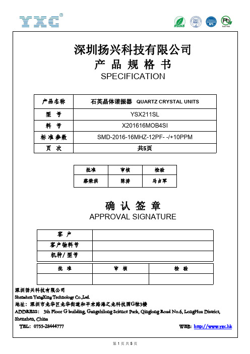
深圳扬兴科技有限公司产品规格书SPECIFICATION产品名称石英晶体谐振器QUARTZ CRYSTAL UNITS型号YSX211SL料号X201616MOB4SI标准参数SMD-2016-16MHZ-12PF--/+10PPM页次共5页批准审核检验蔡荣洪陈涛马占军确认签章APPROVAL SIGNATURE客户客户物料号机种/型号批准审核检验深圳扬兴科技有限公司Shenzhen YangXing Technology Co.,Ltd.地址:深圳市龙华区龙华街道和平东路港之龙科技园G栋3楼ADDRESS:3th Floor G building,Gangzhilong Science Park,Qinglong Road No.6,LongHua District, Shenzhen,ChinaWEB:http://www.yxc.hkREV.版本Description of Revision History修改内容Date日期Engineer工程师Reviewer审核A0.0新版页面修改2021/1/20马占军蔡荣洪A0.1可靠性指标修改2021/1/25马占军蔡荣洪MHz Range Crystal unitYSX211SLProduct name 系列型号YSX211SL16.00000MHz 12PF -/+10.0PPMProduct Number /Ordering code 产品料号X201616MOB4SI1.Absolute maximum ratings Parameter(电气参数)Symbol Min.(最小值)Typ.(典型值)Max.(最大值)Unit (单位)Storage temperature (储存温度)T_stg -55-125ºC Maximum drive level (最大激励功率)GL-100-µW2.Specifications (characteristics)(规格参数)Parameter (电气参数)SymbolMin.(最小值)Typ.(典型值)Max.(最大值)Unit (单位)Type (型号)SEAM 2.0*1.6Oscillation Mode (振动模式)☑Fundamental ☐3rdCutting Mode (切割方式)☑AT☐BT☐X +2°Nominal frequency (标称频率)f_nom -16-MHz Frequency tolerance at 25ºC (常温频差)f_tol -10-10x 10-6Stability Over Temperature (温度稳定性)f_tem -30-30x 10-6Load capacitance(负载电容)CL -12-pF Motional resistance (ESR)(等效谐振电阻)R1--120ΩShunt capacitance (静电容)C0-3-pF Motional capacitance (动态电容)C1-5-fF Level of drive (激励功率)DL -100-µW Operating temperature (工作温度)T_use -40-85ºC Frequency aging (老化率)f_age-3-3x10⁻⁶/year5.Marking information (丝印说明)[1]The suffix "I"in marking stands for operating temperature range between -40℃~+85℃.3.External dimensions (外观尺寸)(Unit:mm)4.Footprint(Recommended)(焊盘推荐)(Unit:mm)YXC ①16.000②028t I③④⑤⑥①YangXing LOGO ⑥Operating Temperature②Frequency ③Year④Production Cycle ⑤Line6.Taping Specification(载带规格)(Unit:mm)Size A B C D E F G H SMD-2016180±2.08.0±0.3 2.30±0.1 1.90±0.1 4.0±0.10.90±0.161.0±1.08.0±1.0 3000pcs per reel7.Reliability characteristic(可靠性)序号检测项目测试要求判定标准1Drop characteristics Free drop from75cm height on a hardwooden board for3times.△f/f≤±5ppm △Rr≤5Ωor15%2Reflow260℃±10℃,Keep10sec△f/f≤±5ppm △Rr≤5Ωor15%3MechanicalshockDevice are shocked to half sine wave(100g)three mutually perpendicular axeseach3times△f/f≤±5ppm△Rr≤5Ωor15%4Shakecharacteristics Shake frequency10~2000Hz,cyc1~2minutes,swing1.5mm,direction x/y/z,each21h all63h test after1hours△f/f≤±5ppm△Rr≤5Ωor15%5Humiditycharacteristics+85℃±2℃&85%~95%R H1000hours△f/f≤±5ppm △Rr≤5Ωor15%6High temperaturecharacteristics +85℃±2℃,1000hours,put in roomtemperature,test after1hours.△f/f≤±5ppm△Rr≤5Ωor15%7Low temperaturecharacteristics -40℃±2℃,250hours,put in roomtemperature,test after1hours.△f/f≤±5ppm△Rr≤5Ωor15%8Temperaturecycling -40±2℃/30min~+125±2℃/30min1000cycles△f/f≤±5ppm△Rr≤5Ωor15%9weldability245℃±10℃,Immersion tin2±05sec Tin leaching rate≥95%10Salt fog The solution concentration is required tobe5%,the temperature is35℃,and theduration is72hNo rust anddelamination第4页共5页Contact uswww.yxc.hk8.Reflow profile (回流焊)Pre Heating TemperatureTp1~Tp2=+170°C Heating TemperatureTMlt =+220°C Peek TemperatureTMax.=+260°CTemperature+260ºCTMax.+220ºCTmlt Point of measuringIn case of Solder ability Terminal.In case of Resistance to soldering heat Surface.Tp2Tp135s100st(time)9.Notice (注意)·包装PACKING·包装方式应符合运输和装卸要求,特殊包装须经双方认可。
AAI-1200S规格书

中海科技(香港)有限公司 AAI-1200S 规格书中海科技(香港)有限公司AAI TECHNOLOGY (HK) LIMITEDSPECIFICATION 产 品 规 格 书DESCRIPTION :DVD MECHA名 称 : DVD 机芯 MODEL : AAI-1200S 型 号 : AAI-1200S CUSTOMER : 客 户 :中海科技(香港)有限公司AAI TECHNOLOGY (HK) LIMITEDTEL: (852) 2692 0790 Fax: (852) 2602 2304 Email:hebin@CUSTOMER APPROVED 客 户 承 认pproved 批准 Checked 确认 Prepared 制作Table of Contents目录1.Scope (3)适用范围2. General Specification (3)一般规格2.1 Applicable Disk Format (3)支持碟片格式2.2 Applicable Disk Capacity (3)支持碟片容量2.3 Applicable Disk Diameter (3)支持碟片直径2.4 Operation Environment (3)工作环境条件2.5 Pick Up Driving Mode (3)光头驱动方式2.6 Feeding Ratio (3)光头移动量2.7 Pick Up Moving Range (3)光头移动范围2.8 Operation Environment (3)工作环境条件2.9 Storage Environment (4)保存环境条件2.10 Dimension (4)外形尺寸2.11 Weight (4)重量3. Optic、Mechanical & Electric Specification (4)光学、机械及电气性能规格3.1 Main Parts (4)主要部品3.2 Optical Specification (4)光学性能规格3.3 Mechanical Specification (4)机械性能规格3.3.1Mechanical Noise (4)机械噪音3.3.2SPINDLE MOTOR (5)主轴马达3.3.3 SLED MOTOR (5)进给马达3.3.4TURN TABLE (5)转盘4. Condition of Performance Evaluation (6)性能评价条件4.1 Install Angle (6)放置角度4.2 Evaluation Environment (6)评价环境4.3 Evaluation disc (6)评价碟片4.4 Evaluation Equipment (6)评价设备5. Reliability Test (6)可靠性保证5.1 Reliability Specification (6)可靠性规格5.2 High Temperature Operation Test (7)高温动作试验5.3 Low Temperature Operation Test (7)低温动作试验5.4 High Temperature Storage Test (7)高温保存试验5.5 Low Temperature Storage Test (7)低温保存试验5.6 Constant Temperature and Humidity Test (7)恒定湿热试验5.7 Swept Vibration Test (7)扫频振动试验5.8 Impact Test (8)碰撞试验5.9 Drop Test (8)跌落试验5.10 Mechanical Life Test (8)机械寿命试验6. Sampling Examination (8)抽样检查7. Standard Quoted (8)引用标准8. Connector Description (8)端子说明9. Caution (9)使用注意事项10. Appendix附录10.1.Connector Description端子说明:(HOP1200S,TT MOTOR,SLED MOTOR)10.2. Mechanical Dimensions产品外形尺寸图10.3. Package Specification包装规格1. Scope适用范围1.1 This specification applies to DVD Mecha for DVD player( model: AAI-1200S).本规格书适用于DVD播放机用的DVD Mecha(型号: AAI-1200S);1.2 Any doubt to the specification can be resolved according to the agreement established withyour relevant department;对本规格书产生疑义时,可依据与贵司的有关部门达成的协议解决;1.3 For improving performance purpose, this specification is subject to change according topre-agreement established between us;为了改善产品性能,本协议书的内容可以依据双方的事前协议进行变更;1.4 Hardware and software or manufacturing process may subject to change for improvements withinthe rang of the specifications;在满足本规格书的范围内,为改善产品性能可能会对硬件、软件或制造工艺进行变更;2. General Specifications一般规格2.1 Applicable Disk Format:支持碟片格式:DVD-5,DVD-9,DVD-10,DVD-18VCD,SVCD,CVD,DVCDCD-DA,MP3CD-R,CD-RW2.2 Applicable Disk Capacity:支持碟片容量:DVD: 4.7GB(DVD-5), 8.5GB(DVD-9),9.4GB(DVD-10),17GB(DVD-18)CD: 650MB(mode 1,12cm),740MB(mode2,12cm),180MB(8cm)2.3 Applicable Disk Diameter: 12cm, 8cm支持碟片直径2.4 Regulate mode : 3Points regulate调整方式: 3点调整2.5 Pick Up Driving Mode : Reduction Gear And Rack Drive光头驱动方式: 3级减速齿轮和齿条驱动2.6 Feeding Ratio: 0.5mm/rev (Sled Motor Rotation One Circle)光头移动量: 0.5 mm/rev (进给马达旋转一周)2.7 Pick Up Moving Range: 22.6±0.3 — 59 ±0.4mm (Begin From Center Of Turn Table)光头移动范围: 22.6±0.3 — 59 ±0.4mm 从转盘中心开始.2.8 Operation Environment工作环境条件Temperature温度0℃~45℃Humidity湿度20%~80%RHAtmospheric pressure大气压85~106KPa2.9 Storage Environment:保存环境条件3.Optic,Mechanical & Electric Specification 光学、机械及电气性能规格 3.1 Main Parts 主要部品3.2 Optical Specification 光学性能规格(PVR520T)3.3 Mechanism Specifications 机械性能规格 3.3.1 Mechanical Noise 机械噪音Background noise is less than 25dB ,measured at 100mm distance, mechanical noise: 背境噪音小于为25dB, 在100mm 距离测量机械噪音Temperature: 温度 -30℃~60℃ Humidity: 湿度5%~90%RH Atmospheric pressure: 大气压85~106KPaSpindle motor: CCM03-030R1-26B 主轴马达Manufacturers: MORETECH 制造商 盟升公司 Sled motor: RF-300CH-11440 进给马达Manufacturers: FF MOTOR 制造商 发发 Pick-up: HOP-1200S 光头 Manufacturers: HITACHI 制造商 日立Specification 规格 Item 项目DVD CDRemarks 备注 Object lens 物镜 Focal distance 焦距(f ) 3.36mm 3.39mm Numerical aperture 数值孔径(NA ) 0.6 0.47 Working distance 动作距离(WD ) 1.71mm 1.35mm Objective emission light 物镜出射光Objective light power (Po ) 出射光功率(Po )0.33mW 0.33mW Typical 典型值 Objective light power (Pmax ) 出射光功率(Pmax )0.5mW 0.5mW Maximum 最大值 Wavelength (λ)出射光波长(λ) 635~665nm 770~810nm JITTER MAX 14% MAX 26nsPlay 播放时 50dB max3.3.2 SPINDLE MOTOR 主轴马达(CCM03-030R1-26B )3.3.3 进给马达(RF-300CH-11440)3.3.4 转盘(TURN TABLE )项 目 规 格备 注TURN TABLE HIGHT 转盘高度 6.8±0.15mm UP FACE OF CHASSIS FOR DATUM PLANE 以CHASSIS 的上表面为基准 TURN TABLE TILTMAX 0.25° 0.25°以下 TURN TABLE RUNOUT 端面跳动 MAX 0.06mm 0.06mm 以下 ECCENTRICITY 偏心 MAX 0.06mm 0.06mm 以下AXIAL LOAD 耐压负荷 MIN 49N (5Kg ) 49N (5Kg )以上BETWEEN TURN TABLE AND MOTOR SHAFT 转盘与马达轴之间耐压力。
AHT21 产品手册说明书

AHT21 产品手册温湿度传感器• 完全标定应用范围暖通空调 、除湿器、测试及检测设备、消费品、汽车 、自动控制、数据记录器、气象站、家电、湿度调节、医疗及其他相关温湿度检测控制。
图 1: AHT21 传感器封装图(单位:mm 公差:±0.1mm )2• 数字输出,I C 接口• 优异的长期稳定性• 采用SMD封装适于回流焊• 响应迅速、抗干扰能力强Top viewFront viewButtom view0.40.553.03.01.02.0Top viewButtom view1.00.50.50.95传感器性能相对湿度温度图 3温度典型误差和最大误差。
±0±2±4±6±8±10图 2 25°C 时相对湿度的最大误差。
△R H (%RH )相对湿度(%RH )电气特性表2 电气特性。
包装信息此精度为出厂检验时,传感器在 25℃供电电压为3.3V 条件下的测试精度。
此数值不包括迟滞和非线性,并只适用于非冷凝条件。
25℃和1m/s 气流条件下,达到一阶响应 63%所需时间。
正常工作范围:0-80%RH, 超出此范围,传感器读数会有偏差(在90%RH 湿度下 200 小时后,漂移<3%RH)。
如果传感器周围有挥发性溶剂、带刺激性气味的胶带、粘合剂以及包装材料,读数可能会偏高。
详细说明请参阅相关文件。
供电电流和功耗的最小值和最大值都是基于 VDD = 3.3V 和 T<60℃的条件。
平均值为每两秒中进行一次测量的数值。
响应时间取决于传感器基片的导热率。
表 1 湿度特性表表 3 温度特性表表4 包装信息。
123456温度(℃)表1中给出的功耗与温度和供电电压VDD有关。
关于功耗的估测参见图6和7。
请注意图6和7中的曲线为典型自然特性,有可能存在偏差。
图6VDD=3.3V时,典型的供电电流与温度的关系曲线(休眠模式)。
3590S-2-502L;3590S-2-102L;3590S-2-103L;3590S-2-203L;3590S-1-502L;中文规格书,Datasheet资料

Specifi cations are subject to change without notice.Customers should verify actual device performance in their specifi c applications.*RoHS Directive 2002/95/EC Jan. 27, 2003 including annex and RoHS Recast 2011/65/EU June 8, 2011.Stop Strength..............................................................................................................................................................................45 N-cm (64 oz.-in.) minimum Mechanical Angle ...........................................................................................................................................................................................3600 ° +10 °, -0 °Torque (Starting & Running) ................................................................................................................................0.35 N-cm (0.5 oz.-in.) maximum (unsealed) 1.1 N-cm (1.5 oz.-in.) maximum (sealed) Mounting ..............................................................................................................................................................................55-80 N-cm (5-7 lb.-in.) (plastic) 90-113 N-cm (8-10 in.-lb.) (metal)Shaft Runout......................................................................................................................................................................................0.13 mm (0.005 in.) teral Runout ...................................................................................................................................................................................0.20 mm (0.008 in.) T.I.R.Shaft End Play ...................................................................................................................................................................................0.25 mm (0.010 in.) T.I.R.Shaft Radial Play ...............................................................................................................................................................................0.13 mm (0.005 in.) T.I.R.Pilot Diameter Runout .......................................................................................................................................................................0.08 mm (0.003 in.) T.I.R.Backlash ............................................................................................................................................................................................................1.0 ° maximum Weight ........................................................................................................................................................................................................Approximately 19 G Terminals ................................................................................................................................................................................................Solder lugs or PC pins Soldering ConditionManual Soldering...........................................................96.5Sn/3.0Ag/0.5Cu solid wire or no-clean rosin cored wire; 370 °C (700 °F) max. for 3 seconds Wave Soldering ...................................................................................96.5Sn/3.0Ag/0.5Cu solder with no-clean fl ux; 260 °C (500 °F) max. for 5 seconds Wash processes .......................................................................................................................................................................................Not recommended Marking .....................................Manufacturer’s name and part number, resistance value and tolerance, linearity tolerance, wiring diagram, and date code.Ganging (Multiple Section Potentiometers) ......................................................................................................................................................1 cup maximum Hardware ............................................................................................................One lockwasher and one mounting nut is shipped with each potentiometer.NOTE: For Anti-rotation pin add 91 after confi guration dash number. Example: -2 becomes -291 to add AR pin.1At room ambient: +25 °C nominal and 50 % relative humidity nominal, except as noted. 2Consult manufacturer for complete specifi cation details for resistances below 1k ohms.BOLDFACE LISTINGS ARE IN STOCK AND READILY AVAILABLETHROUGH DISTRIBUTION. FOR OTHER OPTIONS CONSULT FACTORY.ROHS IDENTIFIER: L = COMPLIANTRecommended Part Numbers(Printed Circuit)(Solder Lug)(Solder Lug)Resistance (Ω)Resolution (%)3590P-2-102L 3590S-2-102L 3590S-1-102L 1,000.0293590P-2-202L 3590S-2-202L 3590S-1-202L 2,000.0233590P-2-502L 3590S-2-502L 3590S-1-502L 5,000.0253590P-2-103L 3590S-2-103L 3590S-1-103L 10,000.0203590P-2-203L 3590S-2-203L 3590S-1-203L 20,000.0193590P-2-503L 3590S-2-503L 3590S-1-503L 50,000.0133590P-2-104L3590S-2-104L3590S-1-104L100,000.009*Ro H S C O MP L I A N T/Panel Thickness Dimensions(For Bushing Mount Only)1.60 +.08/-.03(.063 +.003/-.001)DIA.ANTI-ROTATION PINAnti-rotation pin hole is shown at six o'clockposition for reference only. The actual location isdetermined by the customer's application. Referto the front view of the potentiometer to see thelocation of the optional A/R pin.Panel thickness and hole diameters arerecommended for best fit. However, customersmay adjust the dimensions to suit their specificapplication.Product DimensionsSpecifi cations are subject to change without notice.Customers should verify actual device performance in their specifi c applications.REV. 06/12 MOUNTING SURFACE-2, -4, -6, -8 Confi gurations-1, -3, -5, -7 Confi gurationsRecommended PCB LayoutHOLE DIAMETER5.08(.200)5.08(.200)6.99(.275)SchematicTOLERANCES: EXCEPT WHERE NOTED.508 .127DECIMALS: .XX ±(.02),.XXX ±(.005)FRACTIONS: ±1/64MMDIMENSIONS:(IN.)Shaft & Bushing Confi gurations(Bushing - DxL, Shaft - D):(-1) Plastic Bushing (3/8 ” x 5/16 ”)and Shaft (.2480 + .001, - .002)(-2) Metal Bushing (3/8 ” x 5/16 ”)and Shaft (.2497 + .0000, - .0009)(-3) Sealed, Plastic Bushing (3/8 ” x 5/16 ”)and Shaft (.2480 + .001, - .002)(-4) Sealed, Metal Bushing (3/8 ” x 5/16 ”)and Shaft (.2497 + .0000, - .0009)(-5) Metric, Plastic Bushing (9 mm x 7.94 mm)and Shaft (6 mm + 0, - .076 mm)(-6) Metric, Metal Bushing (9 mm x 7.94 mm)and Shaft (6 mm + 0, - .023 mm)(-7) Metric, Sealed, Plastic Bushing (9 mm x7.94 mm) and Shaft (6 mm + 0, - .076 mm)(-8) Metric, Sealed, Metal Bushing (9 mm x7.94 mm) and Shaft (6 mm + 0, - .023 mm)Terminal Styles“P” Terminal Style“S” Terminal Style/分销商库存信息:BOURNS3590S-2-502L3590S-2-102L3590S-2-103L 3590S-2-203L3590S-1-502L3590S-2-104L 3590S-1-203L3590S-2-501L3590S-2-202L 3590S-1-503L3590S-2-503L3590S-1-104L 3590S-291-102L3590S-291-203L3590S-291-502L 3590S-1-201L3590S-1-501L3590S-2-101L 3590S-2-201L3590P-1-102L3590P-1-103L 3590P-1-201L3590P-1-502L3590S-1-102L 3590S-1-103L3590S-2-252L3590P-291-501L 3590P-2-102L3590P-2-201L3590P-2-203L 3590P-2-502L3590S-1-202L3590S-6-102L 3590S-6-201L3590S-6-202L3590S-6-203L 3590S-6-501L3590P-1-104L3590S-6-502L 3590S-4-102L3590S-4-103L3590S-4-202L 3590S-4-203L3590S-4-502L3590S-8-102L 3590S-8-103L3590S-8-202L3590P-2-104L 3590P-4-103L3590P-4-202L3590S-6-503L 3590S-6-104L3590S-4-104L3590P-4-503L 3590P-4-104L3590S-2-5023590S-1-102 3590S-1-1033590S-1-1043590S-1-203 3590S-1-5023590S-1-5033590S-2-102 3590S-2-1033590S-2-1043590S-2-203 3590S-2-5033590S-1-2023590S-2-202 3590S-2-501。
AMIS30621AUA;中文规格书,Datasheet资料

AMIS-30621Micro-Stepping Motor Driver INTRODUCTIONThe AMIS−30621 is a single−chip micro−stepping motor driver with position controller and control/diagnostic interface. It is ready to build dedicated mechatronics solutions connected remotely with a LIN master.The chip receives positioning instructions through the bus and subsequently drives the motor coils to the desired position. The on−chip position controller is configurable (OTP or RAM) for different motor types, positioning ranges and parameters for speed, acceleration and deceleration. The AMIS−30621 acts as a slave on the LIN bus and the master can fetch specific status information like actual position, error flags, etc. from each individual slave node. The chip is implemented in I2T100 technology, enabling both high voltage analog circuitry and digital functionality on the same chip. The AMIS−30621 is fully compatible with the automotive voltage requirements.PRODUCT FEATURESMotordriver•Micro−Stepping Technology•Peak Current Up to 800 mA•Fixed Frequency PWM Current−Control•Automatic Selection of Fast and Slow Decay Mode•No External Fly−Back Diodes Required•Compliant with 14 V Automotive Systems and Industrial Systems Up to 24 VController with RAM and OTP Memory•Position Controller•Configurable Speeds and Acceleration•Input to Connect Optional Motion SwitchLIN Interface•Physical Layer Compliant to LIN rev. 2.0. Data−Link Layer Compatible with LIN Rev. 1.3 (Note 1)•Field−Programmable Node Addresses •Dynamically Allocated Identifiers •Diagnostics and Status InformationProtection•Overcurrent Protection•Undervoltage Management•Open−Circuit Detection•High Temperature Warning and Management •Low Temperature Flag•LIN Bus Short−Circuit Protection to Supply and Ground •Lost LIN Safe Operation Power Saving•Powerdown Supply Current < 50 m A•5 V Regulator with Wake−up on LIN ActivityEMI Compatibility•LIN Bus Integrated Slope Control•HV Outputs with Slope Control •These are Pb−Free Devices1.Minor exceptions to the conformance of the data−link layer to LIN rev. 1.3.See detailed ordering and shipping information in the package dimensions section on page 2 of this data sheet.ORDERING INFORMATIONSOIC−203 & 7 SUFFIXCASE 751AQNQFP−326 SUFFIXCASE 560AA*For additional information on our Pb−Free strategy and soldering details, please download the ON Semiconductor Soldering and Mounting T echniques Reference Manual, SOLDERRM/D.APPLICATIONSThe AMIS−30621 is ideally suited for small positioning applications. Target markets include: automotive (headlamp alignment, HV AC, idle control, cruise control), industrial equipment (lighting, fluid control, labeling, process control, XYZ tables, robots...) and building automation (HV AC,surveillance, satellite dish, renewable energy systems). Suitable applications typically have multiple axes or require mechatronic solutions with the driver chip mounted directly on the motor.Table 1. ORDERING INFORMATIONPart No.Peak Current UV*Package Shipping†AMIS30621C6213G800 mA High SOIC−20(Pb−Free)Tube / TrayAMIS30621C6213RG800 mA High Tape & ReelAMIS30621C6216G800 mA Low NQFP−32 (7 x 7 mm)(Pb−Free)Tube / TrayAMIS30621C6216RG800 mA Low Tape & ReelAMIS30621C6217G**800 mA Low SOIC−20(Pb−Free)Tube / TrayAMIS30621C6217RG**800 mA Low Tape & Reel†For information on tape and reel specifications, including part orientation and tape sizes, please refer to our Tape and Reel Packaging Specification Brochure, BRD8011/D.*UV undervoltage lock out levels: see DC Parameters UV1 & UV2 (Stop Voltage thresholds).** For prodcut versions AMIS30621C6217G and AMIS30621C6217RG the Ihold0 bit in OTP is programmed to ‘1’.QUICK REFERENCE DATATable 2. ABSOLUTE MAXIMUM RATINGSSymbol Parameter Min Max UnitV BB, VHW2, VSWI Supply voltage, Hardwired Address and SWI Pins−0.3+40(Note 1)VV lin Bus input voltage−40+40VT J Junction temperature range (Note 2)−50+175°CT st Storage temperature−55+160°CV esd Human Body Model Electrostatic discharge voltage on LINpin (Note 3)−4+4kVHuman Body Model Electrostatic discharge voltage on otherpins (Note 3)−2+2kV CDM Electrostatic discharge voltage on other pins (Note 4)−500+500VStresses exceeding Maximum Ratings may damage the device. Maximum Ratings are stress ratings only. Functional operation above the Recommended Operating Conditions is not implied. Extended exposure to stresses above the Recommended Operating Conditions may affect device reliability.1.For limited time: V BB < 0.5 s, SWI and HW2 pins < 1.0 s.2.The circuit functionality is not guaranteed.3.Human Body Model according to MIL−STD−883 Method 3015.7, measured on SOIC devices, and according to AEC−Q100:EIA−JESD22−A114−B (100 pF via 1.5 k W) measured on NQFP device.4.CDM according to EOS_ESD−DS5.3−1993 (draft)−socketed mode, measured on SOIC devices, and according to AEC−Q100:EIA−JESD22−A115−A measured on NQFP devices.Table 3. OPERATING RANGESSymbol Parameter Min Max UnitV BB Supply voltage+6.5+29VT J Operating temperature range (Note 5)−40+165°C5.Note that the thermal warning and shutdown will get active at the level specified in the “DC Parameters”.No more than 100 cumulated hoursin life time above T tw.Table of ContentsGeneral Description 1. . . . . . . . . . . . . . . . . . . . . . . . . . . . Product Features 1. . . . . . . . . . . . . . . . . . . . . . . . . . . . . . Applications 2. . . . . . . . . . . . . . . . . . . . . . . . . . . . . . . . . . Ordering Information 2. . . . . . . . . . . . . . . . . . . . . . . . . . . Quick Reference Data 2. . . . . . . . . . . . . . . . . . . . . . . . . . Maximum Ratings 2. . . . . . . . . . . . . . . . . . . . . . . . . . . . . Block Diagram 3. . . . . . . . . . . . . . . . . . . . . . . . . . . . . . . . Pin Description 4. . . . . . . . . . . . . . . . . . . . . . . . . . . . . . . Package Thermal Resistance 5. . . . . . . . . . . . . . . . . . . . .DC Parameters 6. . . . . . . . . . . . . . . . . . . . . . . . . . . . . . . . AC Parameters 8. . . . . . . . . . . . . . . . . . . . . . . . . . . . . . . . Typical Application 9. . . . . . . . . . . . . . . . . . . . . . . . . . . . Positioning Parameters 10. . . . . . . . . . . . . . . . . . . . . . . . Structural Description 13. . . . . . . . . . . . . . . . . . . . . . . . . Functions Description 14. . . . . . . . . . . . . . . . . . . . . . . . . Lin Controller 33. . . . . . . . . . . . . . . . . . . . . . . . . . . . . . . LIN Application Commands 42. . . . . . . . . . . . . . . . . . . . Package Outline 57. . . . . . . . . . . . . . . . . . . . . . . . . . . . . . Figure 1. Block DiagramTSTLINMOTXP MOTXNHW[2:0]MOTYP MOTYNXP VBB SWI NC HW0XP VBB VBB CPNCPP VCP YN VBB YN VBB VBB YPXNGND GNDXNYPGNDGNDHW1VDDGNDTSTLINHW2GNDNCHW0GND SWI GND HW1MOTXP VBB VDD GND GND MOTXN MOTYP MOTYN TST LIN HW2CPN CPPVBB VCPFigure 2. SOIC −20 and NQFP −32 Pin −outNQFP −32Table 4. PIN DESCRIPTIONPin Name Pin DescriptionSOIC −20NQFP −32HW0Bit 0 of LIN −ADD To be Tied to GND or V DD18HW1Bit 1 of LIN −ADD29V DD Internal supply (needs external decoupling capacitor)310GND Ground, heat sink4,7,14,1711, 14, 25, 26, 31, 32TST Test pin (to be tied to ground in normal operation)512LIN LIN −bus connection 613HW2Bit 2 LIN −ADD815CPN Negative connection of pump capacitor (charge pump)917CPP Positive connection of pump −capacitor (charge pump)1018VCP Charge −pump filter −capacitor 1119V BB Battery voltage supply 12,193, 4, 5, 20, 21, 22MOTYN Negative end of phase Y coil 1323, 24MOTYP Positive end of phase Y coil 1527, 28MOTXN Negative end of phase X coil 1629, 30MOTXP Positive end of phase X coil 181, 2SWI Switch input206NCNot connected (to be tied to ground)7, 16PACKAGE THERMAL RESISTANCEThe AMIS −30621 is available in SOIC −20 and optimized NQFP32 packages. For cooling optimizations, the NQFP has an exposed thermal pad which has to be soldered to the PCB ground plane. The ground plane needs thermal vias to conduct the head to the bottom layer. Figures 3 and 4 give examples for good power distribution solutions.For precise thermal cooling calculations the major thermal resistances of the devices are given. The thermal media to which the power of the devices has to be given are:•Static environmental air (via the case)•PCB board copper area (via the device pins and exposed pad)The thermal resistances are presented in Table 5: DC Parameters.The major thermal resistances of the device are the Rth from the junction to the ambient (Rthja) and the overall Rth from the junction to the leads (Rthjp).The NQFP device is designed to provide superior thermal performance. Using an exposed die pad on the bottom surface of the package, is mainly contributing to this performance. In order to take full advantage of the exposed pad, it is most important that the PCB has features to conduct heat away from the package. A thermal grounded pad with thermal vias can achieve this.In below table, one can find the values for the Rthja and Rthjp, simulated according to the JESD −51standard:Package RthJunction −to −Leads and Exposed Pad (Rthjp)RthJunction −to −Leads(Rthjp)RthJunction −to −AmbientRthja 1S0PRthJunction −to −AmbientRthja 2S2PSOIC −20 196239NQFP −320.956030The Rthja for 2S2P is simulated conform to JESD −51 as follows:•A 4−layer printed circuit board with inner power planes and outer (top and bottom) signal layers is used •Board thickness is 1.46 mm (FR4 PCB material)•The 2 signal layers: 70 m m thick copper with an area of 5500 mm2 copper and 20% conductivity•The 2 power internal planes: 36 m m thick copper with an area of 5500 mm 2 copper and 90% conductivityThe Rthja for 1S0P is simulated conform to JESD −51 as follows:•A 1−layer printed circuit board with only 1 layer •Board thickness is 1.46 mm (FR4 PCB material)•The layer has a thickness of 70 m m copper with an area of 5500 mm 2 copper and 20% conductivityFigure 3. Example of SOIC −20 PCB Ground Plane Layout (Preferred Layout at Top and Bottom)Figure 4. Example of NQFP −32 PCB Ground Plane Layout (Preferred Layout at Top and Bottom)DC PARAMETERSThe DC parameters are guaranteed over temperature and V BB in the operating range, unless otherwise specified. Convention: currents flowing into the circuit are defined as positive.Table 5. DC PARAMETERSSymbol Pins Parameter Test Conditions Min Typ Max Unit MOTORDRIVERI MSmax,PeakMOTXPMOTXNMOTYPMOTYN Max current through motorcoil in normal operationV BB = 14 V800mAI MSmax,RMS Max RMS Current ThroughCoil in Normal OperationV BB = 14 V570mAI MSabs Absolute Error on Coil Current(Note 6)V BB = 14 V−1010%I MSrel Matching of X and Y CoilCurrentsV BB = 14 V−707%R DS(on)On Resistance for Each MotorPin at I MSmax (Note 7)V BB = 12 V, T J = 50°C0.501W V BB = 8 V, T J = 50°C0.551W V BB = 12 V, T J = 150°C0.701W V BB = 8 V, T J = 150°C0.851WI MSL Pull down current HiZ Mode, V BB = 7.7 V0.4 2.2mA LIN TRANSMITTERI bus_offLIN Dominant State, Driver Off V bus = 0 V, V BB = 8 V and 18 V−1mAI bus_off Recessive State, Driver Off V bus = V bat,V BB = 8 V and 18 V20m A I bus_lim Current Limitation V BB = 8 V and 18 V5075130mA R slave Pullup Resistance V BB = 8 V and 18 V203047k W LIN RECEIVERV bus_domLIN Receiver Dominant State V BB = 8 V and 18 V00.4 * V BB VV bus_rec Receiver Recessive State V BB = 8 V and 18 V0.6 * V BB V BB V V bus_hys Receiver Hysteresis V BB = 8 V and 18 V0.05 * V BB0.175 * V BB V THERMAL WARNING AND SHUTDOWNT tw Thermal warning138145152°C T tsd Thermal shutdown(Notes 8 and 9)T tw + 10°CT low Low temperature warning(Note 9)T tw− 152°C SUPPLY AND VOLTAGE REGULATORV BBOTPV BB Supply voltage for OTPzapping (Note 10)9.010.0VUV1Stop voltage high threshold Product versions with low UV;See Ordering Information7.78.38.9V UV2Stop voltage low threshold7.07.58.0V UV1Stop voltage high threshold Product versions with high UV;See Ordering Information8.89.39.8V UV2Stop voltage low threshold8.18.58.9V I bat Total current consumption Unloaded outputsV BB = 29 V1 3.5010.0mAI bat_s Sleep mode currentconsumptionV BB = 8 V and 18 V40100m AV DDV DD Regulated internal supply(Note 11)8 V < V BB < 29 V 4.755 5.25VV DDReset Digital supply reset level @powerdown (Note 12)4.5VI DDLim Current limitation Pin shorted to groundV BB = 14 V40mATable 5. DC PARAMETERSSymbol UnitMaxTypMinTest ConditionsParameterPinsSWITCH INPUT AND HARDWIRE ADDRESS INPUTRt_OFFSWI HW2Switch OPEN Resistance(Note 13)10k WRt_ON Switch ON Resistance(Note 13)Switch to GND or V BB2k WV BB_sw V BB range for guaranteedoperation of SWI and HW2629VI lim_sw Current limitation Short to GND or V batV BB = 29 V45mA HARDWIRED ADDRESS INPUTS AND TEST PINV highHW0HW1 TST Input level high V BB = 14 V0.7 * V DD VV low Input level low V BB = 14 V0.3 * V DD V HW hyst Hysteresis V BB = 14 V0.075 * V DD V CHARGE PUMPV CPVCP Output voltage7 V < V BB v 14 V 2 * V BB−2.5V14 V < V BB V BB + 10V BB + 15VC buffer External buffer capacitor220470nF C pump CPP CPN External pump capacitor220470nF PACKAGE THERMAL RESISTANCE VALUESRth ja SO Thermal resistancejunction−to−ambient (2S2P)Simulated conform JEDECJES.D5139K/WRth jp SO Thermal resistancejunction−to−leads19K/WRth ja NQ Thermal resistancejunction−to−ambient (2S2P)30K/WRth jpNQ Thermal resistancejunction−to−leads andexposed pad0.95K/W6.Tested in production for 800 mA, 400 mA, 200 mA and 100 mA current settings for both X and Y coil.7.Based on characterization data.8.No more than 100 cumulated hours in life time above T tw.9.Thermal shutdown and low temperature warning are derived from thermal warning. Guaranteed by design.10.A buffer capacitor of minimum 100 m F is needed between V BB and GND. Short connections to the power supply are recommended.11.Pin V DD must not be used for any external supply12.The RAM content will not be altered above this voltage.13.External resistance value seen from pin SWI or HW2, including 1 k W series resistor. For the switch OPEN, the maximum allowed leakagecurrent is represented by a minimum resistance seen from the pin.AC PARAMETERSThe AC parameters are guaranteed for temperature and V BB in the operating range unless otherwise specified.The LIN transmitter and receiver physical layer parameters are compliant to LIN rev. 2.0 & 2.1.Table 6. AC PARAMETERSSymbol Pins Parameter Test Conditions Min Typ Max Unit POWERUPT pu Powerup Time Guaranteed by Design10ms INTERNAL OSCILLATORf osc Frequency of Internal Oscillator V BB = 14 V 3.6 4.0 4.4MHz LIN TRANSMITTER CHARACTERISTICS ACCORDING TO LIN V2.0 & V2.1D1LIN Duty Cycle 1 = t Bus_rec(min)/(2 x t Bit); See Figure 5THRec(max)= 0.744 x V BBTHDom(max)= 0.581 x V BB;V BB = 7.0 V...18 V; t Bit =50 m s0.396D2Duty Cycle 2 = t Bus_rec(max)/(2 x t Bit); See Figure 5THRec(min)= 0.284 x V BBTHDom(min)= 0.422 x V BB;V BB = 7.6 V...18 V;t Bit = 50 m s0.581LIN RECEIVER CHARACTERISTICS ACCORDING TO LIN V2.0 & V2.1trx_pdrLIN Propagation delay bus dominantto RxD = LowV BB = 7.0 V & 18 V;See Figure 56m strx_pdf Propagation delay bus recess-ive to RxD = High V BB = 7.0 V & 18 V;See Figure 56m strx_sym Symmetry of receiver propaga-tion delaytrx_pdr – trx_pdf−2+2m s SWITCH INPUT AND HARDWIRE ADDRESS INPUTT sw SWIHW2Scan pulse period (Note 14)V BB = 14 V1024m sT sw_on Scan pulse duration (Note 14)V BB = 14 V64m s MOTORDRIVERF pwmMOTxx PWM frequency (Note 14)182022.0kHzT brise Turn−on transient time Between 10% and 90%V BB = 14 V 150nsT bfall Turn−off transient time140ns T stab Run current stabilization time(Note 14)1/Vmin s CHARGE PUMPf CP CPNCPP Charge pump frequency(Note 14)V BB = 14 V250kHz14.Derived from the internal oscillatorFigure 5. Timing Diagram for AC Characteristics According to LIN 2.0 & 2.1LINtRxD TxDttTH Rec(max)TH Dom(max)TH Rec(min)TH Dom(min)TYPICAL APPLICATIONFigure 6. Typical Application Diagram for SO device.LIN busV BATConnect to V BAT or GND Connect to V BAT or GND15.All resistors are ±5%, 1/4 W16.C 1, C 2 minimum value is 2.7 nF, maximum value is 10 nF17.Depending on the application, the ESR value and working voltage of C 7 must be carefully chosen 18.C 3 and C 4 must be close to pins V BB and GND19.C 5 and C 6 must be as close as possible to pins CPN, CPP , VCP , and V BB to reduce EMC radiation 20.C 9 must be a ceramic capacitor to assure low ESR21.C 10 is placed for EMC reasons; value depends on EMC requirements of the applicationPOSITIONING PARAMETERSStepping ModesOne of four possible stepping modes can be programmed:•Half−stepping•1/4 micro−stepping•1/8 micro−stepping•1/16 micro−stepping Maximum VelocityFor each stepping mode, the maximum velocity Vmax can be programmed to 16 possible values given in the table below.The accuracy of Vmax is derived from the internal oscillator. Under special circumstances it is possible to change the V max parameter while a motion is ongoing. All 16 entries for the Vmax parameter are divided into four groups. When changing Vmax during a motion the application must take care that the new Vmax parameter stays within the same group.Table 7. MAXIMUM VELOCITY SELECTION TABLEVmax indexVmax(full step/s)Group Stepping modeHex Dec Half−stepping(half−step/s)1/4thMicro−stepping(micro−step/s)1/8thMicro−stepping(micro−step/s)1/16thMicro−stepping(micro−step/s)0099A197395790157911136B 273546109121822216733466813352670 3319739579015793159 4421342585117013403 5522845691218233647 662434869731945389177273C 54610912182436488303607121324264852 99334668133526705341 A10364729145729145829 B11395790157931596317 C12456912182336477294D13546D 1091218243648728E1472914572914582911658 F1597319453891778215564分销商库存信息: ONSEMIAMIS30621AUA。
- 1、下载文档前请自行甄别文档内容的完整性,平台不提供额外的编辑、内容补充、找答案等附加服务。
- 2、"仅部分预览"的文档,不可在线预览部分如存在完整性等问题,可反馈申请退款(可完整预览的文档不适用该条件!)。
- 3、如文档侵犯您的权益,请联系客服反馈,我们会尽快为您处理(人工客服工作时间:9:00-18:30)。
5. As silicone encapsulation is permeable to gases, some corrosive substances such as H2S might corrode silver plating of leadframe. Special care should be taken if an LED with silicone encapsulation is to be used near such substances. SPEC NO: DSAL0968 APPROVED: WYNEC REV NO: V.2 CHECKED: Allen Liu DATE: MAR/18/2011 DRAWN: J.Yu PAGE: 2 OF 6 ERP: 1201007016
REV NO: V.2 CHECKED: Allen Liu
DATE: MAR/18/2011 DRAWN: J.Yu
PAGE: 6 OF 6 ERP: 1201007016
芯天下--/
DATE: MAR/18/2011 DRAWN: J.Yu
PAGE: 4 OF 6 ERP: 1201007016
芯天下--/
AA3021YS
Reflow soldering is recommended and the soldering profile is shown below. Other soldering methods are not recommended as they might cause damage to the product.
Notes: 1. All dimensions are in millimeters (inches). 2. Tolerance is ±0.2(0.008") unless otherwise noted. 3. The specifications, characteristics and technical data described in the datasheet are subject to change without prior notice. 4. The device has a single mounting surface. The device must be mounted according to the specifications.
2. Do not directly touch or handle the silicone lens surface. It may damage the internal circuitry.
3. Do not stack together assembled PCBs containing exposed LEDs. Impact may scratch the silicone lens or damage the internal circuitry.
DATE: MAR/18/2011 DRAWN: J.Yu
PAGE: 3 OF 6 ERP: 1201007016
芯天下--/
Yellow
AA3021YS
SPEC NO: DSAL0968 APPROVED: WYNEC
REV NO: V.2 CHECKED: Allen Liu
芯天下--/
Selection Guide
Part No. Dice Lens Type Iv (mcd) [2] @ 20mA Min. AA3021YS Yellow (GaAsP/GaP) Water Clear 8 Typ. 15 Viewing Angle [1] 2θ1/2 125°
Notes: 1.Wavelength: +/-1nm. 2. Forward Voltage: +/-0.1V.
Absolute Maximum Ratings at TA=25°C
Parameter Power dissipation DC Forward Current Peak Forward Current [1] Reverse Voltage Operating Temperature Storage Temperature
Note: 1. 1/10 Duty Cycle, 0.1ms Pulse Width.
Yellow 75 30 140 5 -40°C To +85°C -40°C To +85°C
Units mW mA mA V
SPEC NO: DSAL0968 APPROVED: WYNEC
REV NO: V.2 CHECKED: Allen Liu
Recommended Soldering Pattern (Units : mm; Tolerance: ± 0.1)
Reel Dimension
Tape Dimensions (Units : mm)
SPEC NO: DSAL0968 APPROVED: WYNEC
REV NO: V.2 CHECKED: Allen Liu
3.0x2.0mm SURFACE MOUNT LED LAMP
Part Number: AA3021YS Yellow
Features
3.0mm x 2.0mm, 1.3mm high, only minimum space required. Suitable for compact optoelectronic applications. Low power consumption. Package : 2000pcs / reel. Moisture sensitivity level : level 3. RoHS compliant.
SPEC NO: DSAL0968 APPROVED: WYNEC
REV NO: V.2 CHECKED: Allen Liu
DATE: MAR/18/2011 DRAWN: J.Yu
PAGE: 1 OF 6 ERP: 1201007016
芯天下--/
Handling Precautions
Description
The Yellow source color devices are made with n Gallium Phosphide Yellow Light Emitting Diode.
Package Dimensions
Notes: 1. θ1/2 is the angle from optical centerline where the luminous intensity is 1/2 of the optical peak value. 2. Luminous intensity/ luminous Flux: +/-15%.
DATE: MAR/18/2011 DRAWN: J.Yu
PAGE: 5 OF 6 ERP: 1201007016
芯天下--/
PACKING & LABEL SPECIFICATIONS
AA3021YS
SPEC NO: DSAL0968 APPROVED: WYNEC
Electrical / Optical Characteristics at TA=25°C
Symbol λpeak λD [1] Δλ1/2 C VF [2] IR Parameter Peak Wavelength Dominant Wavelength Spectral Line Half-width Capacitance Forward Voltage Reverse Current Device Yellow Yellow Yellow Yellow Yellow Yellow Typ. 590 588 35 20 2.1 2.5 10 Max. Units nm nm nm pF V uA Test Conditions IF=20mA IF=20mA IF=20mA VF=0V;f=1MHz IF=20mA VR=5V
Compare to epoxy encapsulant that is hard and brittle, silicone is softer and flexible. Although its characteristic significantly reduces thermal stress, it is more susceptible to damage by external mechanical force. As a result, special handling precautions need to be observed during assembly using silicone encapsulated LED products. Failure to comply might lead to damage and premature failure of the LED. 1. Handle the component along the side surfaces by using forceps or appropriate tools.
4.1. The outer diameter of the SMD pickup nozzle should not exceed the size of the LED to prevent air leaks. The inner diameter of the nozzle should be as large as possible. 4.2. A pliable material is suggested for the nozzle tip to avoid scratching or damaging the LED surface during pickup. 4.3. The dimensions of the component must be accurately programmed in the pick-and-place machine to insure precise pickup and avoid damage during production.