EqDiff1_EFS_jan2009_corr
[实用贴]西门子磁共振序列命名规则,看了涨N年功力!
![[实用贴]西门子磁共振序列命名规则,看了涨N年功力!](https://img.taocdn.com/s3/m/e88fb11aeef9aef8941ea76e58fafab069dc4485.png)
[实用贴]西门子磁共振序列命名规则,看了涨N年功力!来源: MR应用爱影之家序列类型的后缀比较简单,就是“R(快速恢复)”、“B(刀锋技术)”和“_r*(流动补偿系列)”三种。
“_r*(流动补偿系列)”有以下几种方式1._r:完全流动补偿(在读出及层面方向均进行流动补偿)2._rr:仅在读出方向上进行流动补偿3._rs:仅在层面方向上进行流动补偿4._rd:利用交互的重复时相及去时相检测来进行的交互存取采集se 自旋回波se_r 带流动补偿的自旋回波tse 快速自旋回波tse_rr 读出方向上进行流动补偿的快速自旋回波tseB 使用刀锋技术的快速自旋回波tseR 带快速恢复脉冲的快速自旋回波tseBR 使用刀锋技术和快速恢复脉冲的快速自旋回波tseR_rr 带快速恢复脉冲并在读出方向上进行流动补偿的的快速自旋回波tir 带反转脉冲的快速自旋回波tir_rr 读出方向上进行流动补偿的带反转脉冲的快速自旋回波tirB 使用刀锋技术的带反转脉冲的快速自旋回波tirBR 使用刀锋技术并带快速恢复脉冲及反转脉冲的快速自旋回波spc 可变翻转角快速自旋回波spcir 带反转恢复脉冲的可变翻转角快速自旋回波spcir_r 带反转恢复脉冲和流动补偿技术的可变翻转角快速自旋回波spcR 带快速恢复脉冲的可变翻转角快速自旋回波spcR_rr 带快速恢复脉冲和读出方向上流动补偿的可变翻转角快速自旋回波h 半傅里叶采集单次激发快速自旋回波hir 带反转脉冲的半傅里叶采集单次激发快速自旋回波fl 快速小角度激发fl_r 带流动补偿技术的快速小角度激发fl_rd 带交互式流动补偿技术的快速小角度激发tfl 带有磁化准备脉冲的快速小角度激发swi_r 带有磁敏感加权成像技术和流动补偿技术的快速小角度激发pc 相位对比法MRAfi 稳态进动快速成像tfi 真稳态进动快速成像ps_rr 读出方向上流动补偿的时间反转FISPme_r 多回波合并成像epfid 梯度回波EPIepir 带反转脉冲的EPIepse 自旋回波EPI序列名的后缀一般是“_*”形式,常见的有:_vfl:可变翻转角_vibe:容积内插体部扫描_pc:时相对比法MRA_tof:时间飞跃法MRA_ce:增强扫描_diff:弥散成像_rd:流动补偿(利用交互的重复时相及去时相检测来进行的交互存取采集)_se:自旋回波_bold:血氧合水平依赖比较特殊的是自旋回波序列(SE),其序列名可以为“se_15b130”或“se_17rb130”,“b130”指的是带宽,“r”指的是有流动补偿,无“r”则无流动补偿。
JEDEC_JS709-A JOINT JEDEC_ECA STANDARD, DEFINING “LOW-HALOGEN” ELECTRONIC PRODUCTS (REMOVAL OF BFR

JEDEC standards and publications are adopted without regard to whether or not their adoption may involve patents or articles, materials, or processes. By such action JEDEC does not assume any liability to any patent owner, nor does it assume any obligation whatever to parties adopting
Standards and Documents for alternative co源自tact information.
Published by ©JEDEC Solid State Technology Association 2012
3103 North 10th Street Suite 240 South
3
4
Requirements for low-halogen electronic products
5
5
Compliance process for low-halogen electronic materials and components
5
6
Marking and labeling for low-halogen electronic products
______________________________________Contents_______________________________________
【WO2019217850A1】基于光调制器和相干接收器的用于同时距离和速度测量的激光雷达系统【专利

) (1(51)International Patent Classification:(74)Agent:HAGGERSON,Michael et al.;K&l Gates LLP,G01S17/02(2006.01)G01S17/06(2006.01)210Sixth Avenue,K&l Gates Center,Pittsburgh,PA G01J9/04(2006.01)G01S17/42(2006.01)15222-2613(US).G01S17/00(2006.01)G01S17/88(2006.01)(81)Designated States(unless otherwise indicated,for every (21)International Application Number:kind o f national protection av ailable).AE,AG,AL,AM,PCT/US2019/031767AO,AT,AU,AZ,BA,BB,BG,BH,BN,BR,BW,BY,BZ,CA,CH,CL,CN,CO,CR,CU,CZ,DE,DJ,DK,DM,DO, (22)International Filing Date:DZ,EC,EE,EG,ES,FI,GB,GD,GE,GH,GM,GT,HN,10May2019(10.05.2019)HR,HU,ID,IL,IN,IR,IS,JO,JP,KE,KG,KH,KN,KP, (25)Filing Language:English KR,KW,KZ,LA,LC,LK,LR,LS,LU,LY,MA,MD,ME,MG,MK,MN,MW,MX,MY,MZ,NA,NG,NI,NO,NZ, (26)Publication Language:English OM,PA,PE,PG,PH,PL,PT,QA,RO,RS,RU,RW,SA, (30)Priority Data:SC,SD,SE,SG,SK,SL,SM,ST,SV,SY,TH,TJ,TM,TN,62/669,80310May2018(10.05.2018)US TR,TT,TZ,UA,UG,US,UZ,VC,VN,ZA,ZM,ZW.62/669,80810May2018(10.05.2018)US(84)Designated States(unless otherwise indicated,for every62/669,80110May2018(10.05.2018)US kind o f regional protectionavailable).ARIPO(BW,GH, (71)Applicant:OURS TECHNOLOGY,INC.[US/US];288GM,KE,LR,LS,MW,MZ,NA,RW,SD,SL,ST,SZ,TZ,Church Street,No.1,Mountain View,CA94041(US).UG,ZM,ZW),Eurasian(AM,AZ,BY,KG,KZ,RU,TJ,TM),European(AL,AT,BE,BG,CH,CY,CZ,DE,DK, (72)Inventors:SANDBOM,Phillip;288Church Street,No.1,EE,ES,FI,FR,GB,GR,HR,HU,IE,IS,IT,LT,LU,LV,Mountain View,CA94041(US).LIN,Sen;288Church MC,MK,MT,NL,NO,PL,PT,RO,RS,SE,SI,SK,SM, Street,No.1,Mountain View,CA94041(US).TR),OAPI(BF,BJ,CF,CG,Cl,CM,GA,GN,GQ,GW,KM,ML,MR,NE,SN,TD,TG).(54)Title:LIDAR SYSTEM BASED ON LIGHT MODULATOR AND COHERENT RECEIVER FOR SIMULTANEOUS RANGE AND VELOCITY MEASUREMENTFIG.1123(57)Abstract:A LIDAR system and method for determining a distance and a velocity of a target.The LIDAR system can include a laser modulated by a laser modulator,an optical combiner,an optical splitter,a photoreceiver,and a control circuit.The optical splitter can optically split the modulated laser beam into a first laser beam and a second laser beam and direct the first laser beam at the target such that the first laser beam is reflected by the target to the optical combiner.The optical combiner can optically combine the first laser beam and the second laser beam.The output an I-output and a Q-output according to the optically combined first laser beam and second laser beam.The control circuit can determine a nominal beat frequency,which corresponds to the distance of the target,and a frequency shift,which corresponds to the velocity of the target,accordingly.[Continued on next page]W O2019/217850A1 Published:with international search report(Art.21(3))with amended claims(Art.19(1))。
智能融合cSoC:多通道FFT共享处理器使用FPGA纤维说明书

Application Note AC381February 20121© 2012 Microsemi Corporation SmartFusion cSoC: Multi-Channel FFT Co-Processor Using FPGA FabricTable of ContentsIntroductionThe SmartFusion ® customizable system-on-chip (cSoC) device integrates FPGA technology with a hardened ARM ® Cortex™-M3 processor based microcontroller subsystem (MSS) and programmable high-performance analog blocks built on a low power flash semiconductor process. The MSS consists of hardened blocks such as a 100 MHz ARM Cortex-M3 processor, peripheral direct memory access (PDMA), embedded nonvolatile memory (eNVM), embedded SRAM (eSRAM), embedded FlashROM (eFROM), external memory controller (EMC), Watchdog Timer, the Philips Inter-Integrated Circuit (I 2C),serial peripheral interface (SPI), 10/100 Ethernet controller, real-time counter (RTC), GPIO block, fabric interface controller (FIC), in-application programming (IAP), and analog compute engine (ACE).The SmartFusion cSoC device is a good fit for applications that require interface with many analog sensors and analog channels. SmartFusion cSoC devices have a versatile analog front-end (AFE) that complements the ARM Cortex-M3 processor based MSS and general-purpose FPGA fabric. The SmartFusion AFE includes three 12-bit successive approximation register (SAR) ADCs, one first order sigma-delta DAC (SDD) per ADC, high performance signal conditioning blocks, and comparators. The SmartFusion cSoCs have a sophisticated controller for the AFE called the ACE. The ACE configures and sequences all the analog functions using the sample sequencing engine (SSE) and post-processes the results using the post processing engine (PPE) and handles without intervention of Cortex-M3 processor.Refer to the SmartFusion Programmable Analog User’s Guide for more details.This application note describes the capability of SmartFusion cSoC devices to compute the Fast Fourier Transform (FFT) in real time. The Multi Channel FFT example design can be used in medical applications, sensor network applications, multi channel audio Spectrum analyzers, Smart Metering, and sensing applications (such as vibration analysis).This example design uses the Cortex-M3 processor in the SmartFusion MSS as a master and the FFT processor in the FPGA fabric as a slave. All three of the SmartFusion cSoC A2F500’s ADCs are used for data acquisition. The example design uses Microsemi’s CoreFFT IP and the advanced peripheral bus interface (CoreAPB3). A custom-made APB3 interface has been developed to connect CoreFFT with the MSS via CoreAPB3. The Cortex-M3 processor uses the PDMA controller in the MSS for the data transfer and thus helps to free up the Cortex-M3 processor instruction bandwidth.A basic understanding of the SmartFusion design flow is assumed. Refer to Using UART with SmartFusion - Microsemi Libero ® SoC and SoftConsole Flow Tutorial to understand the SmartFusion design flow.Introduction . . . . . . . . . . . . . . . . . . . . . . . . . . . . . . . . . . . . . . . . . . . . . . . . 1Design Overview . . . . . . . . . . . . . . . . . . . . . . . . . . . . . . . . . . . . . . . . . . . . . 2Design Description . . . . . . . . . . . . . . . . . . . . . . . . . . . . . . . . . . . . . . . . . . . . 2Implementing Multi Channel FFT on EVAL KIT BOARD . . . . . . . . . . . . . . . . . . . . . . . . . 7Running the Design . . . . . . . . . . . . . . . . . . . . . . . . . . . . . . . . . . . . . . . . . . . . 8Conclusion . . . . . . . . . . . . . . . . . . . . . . . . . . . . . . . . . . . . . . . . . . . . . . . . 9Appendix A – Design Files . . . . . . . . . . . . . . . . . . . . . . . . . . . . . . . . . . . . . . . 10SmartFusion cSoC: Multi-Channel FFT Co-Processor Using FPGA Fabric2Design OverviewThis design example demonstrates the capability of the SmartFusion cSoC device to compute the FFT for multiple data channels. The FFT computation is a complex task that utilizes extensive logic resources and computation time. In general, for N number of channels, N number of FFT IP’s are needed to be instantiated, which in turn utilize more logic resources on the FPGA. A way to avoid this limitation is to use the same FFT logic for multiple input channels.This design illustrates the implementation of a Multichannel FFT to process multiple data channels through a single FFT and store FFT points in a buffer. The FFT computes the input data read from each channel and stores the N-point result in the respective channel’s allocated buffer. The channel multiplexing is done once each channel buffer has been loaded with the FFT length.Computing frequency components for a real time data of six channels is described in this application note. For sampling the input signals the AFE is used and the complex FFT computation is implemented in the fabric of the SmartFusion cSoC device. The Cortex-M3 processor in the MSS of the SmartFusion cSoC handles the buffer management and channel muxing.Figure 1 depicts the block diagram of six channel FFT co-processor in FPGA fabric.Design DescriptionThe design uses CoreFFT for computing the FFT results. You can download the core generator for CoreFFT at /soc/portal/default.aspx?r=4&p=m=624,ev=60.The design example uses a 512-point and 16-bit FFT. A custom-made APB3 interface has been developed to connect CoreFFT IP with the MSS’s FIC. The CoreFFT output data is stored in a 512x32FIFO within the fabric. The FIFO status signals are given in Table 1 on page 3. The status signals indicate that FFT is ready to receive data and data is available in the output of FIFO. These status signals are mapped to the GPIOs in the MSS. The Cortex-M3 processor can read the GPIOs to handle flow control in the data transfer process from the MSS to CoreFFT.Figure 1 • Multi Channel FFT Block DiagramDesign Description3Figure 2 shows the block diagram of logic in the fabric with custom-made APB3 bus.The data valid signal (ifiD_valid) is generated in custom logic whenever the master needs to write data into the input buffer of the FFT to process through the APB3 interface. The FFT_IP_RDY signal indicates the status of the input buffer of the FFT. If the input buffer is full, the FFT_IP_RDY goes low. The master can read the FFT_IP_RDY signal to get the FFT input buffer status. The FFT generates the processed data with a data valid signal (ifoY_valid). The processed data is stored in the FIFO. When FIFO is not ready to receive output data, it can stop the data fetching from the FFT by pulling down the ifiRead_y signal. The status signal FFT_OP_RDY is used to indicate to the master that processed data is available in the FIFO. FFT_OP_RDY goes High whenever processed data is available in the FFT output buffer.The master can use AEMPTY_OUT or EMPTY_OUT to determine whether the FIFO is empty and all the processed data has been read. Refer to the CoreFFT Handbook for more details on architecture and interface signal descriptions.Three ADCs are configured to have two channels, each channel with 100 ksps sampling rate. The external memory is used for input and output buffers. For each channel, one input buffer having length double to the length of FFT i.e. 1024 words and one output buffer having length equal to the length of FFT i.e. 512 words are used. After each channel's input buffer has 512 points required for the full length of the FFT, each channel, one after the other, streams its points from the FIFO through the FFT. During the FFT computational period, the sampled data values of each channel are stored in the second half of the input buffer. Once the FFT computations for the First half of input buffer completes then the points in the second half of the input buffer will be streamed to FFT. This operation utilizes a ping-pong method. The Cortex-M3 processor is used for data management, that is, buffering the sampled points and data routing or muxing of these values to the FFT computation block. Sampling of the real time data is done by the ACE. The PDMA handles the data transfer between the external SRAM (eSRAM) buffers and CoreFFT logic in FPGA fabric.Figure 2 • CoreFFT with APB Slave InterfaceTable 1 • FIFO Status Signals with DescriptionsSignalDescription FFT_IP_RDYFFT is ready to receive the Input from the master processor FFT_OP_RDYProcessed data is ready in output buffer of FFT AEMPTY_OUTOutput FIFO is almost empty EMPTY_OUT Output FIFO is emptySmartFusion cSoC: Multi-Channel FFT Co-Processor Using FPGA Fabric4Figure 3 shows the implementation of multi channel FFT on the SmartFusion cSoC device.Hardware ImplementationThe MSS is configured with an FIC, clock conditioning circuit (CCC), GPIOs, EMC and a UART. The CCC generates 80 MHz clock, which acts as the clock source. The FIC is configured to use a master interface with an AMBA APB3 interface. Four GPIOs in the MSS are configured as inputs that are used to handle flow control in data transfer from MSS to FFT coprocessor. The EMC is configured for Region 0as Asynchronous RAM and port size as half word. The UART_0 is configured for printing the FFT values to the PC though a serial terminal emulation program.ADC0, ADC1, and ADC2 are configured with 12-bit resolution, two channels and the sampling rate is set to approximately 100 KHz. Figure 4 on page 5 shows the ACE configuration window.Figure 3 • Implementation of Multi Channel FFT on the SmartFusion cSoCDesign Description5The APB wrapper logic is implemented on the top of CoreFFT and connected to CoreAPB3. A FIFO of size 512*32 is used to connect to CoreFFT output.CoreAPB3 acts as a bridge between the MSS and the FFT coprocessor block. It provides an advanced microcontroller bus architecture (AMBA3) advanced peripheral bus (APB3) fabric supporting up to 16APB slaves. This design example uses one slave slot (Slot 0) to interface with the FFT coprocessor block and is configured with direct addressing mode. Refer to the CoreAPB3 Handbook for more details on CoreAPB3 IP .For more details on how to connect FPGA logic MSS, refer to the Connecting User Logic to the SmartFusion Microcontroller Subsystem application note.The logic in the FPGA fabric consumes 18 RAM blocks out of 24. We cannot use eSRAM blocks for implementing CoreFFT as the transactions between these SRAM blocks and FFT logic are very high and are time critical.Figure 5 on page 6 illustrates the multi channel FFT example design in the SmartDesign.Figure 4 • Configure ACESmartFusion cSoC: Multi-Channel FFT Co-Processor Using FPGA Fabric6Table 2 summarizes the logic resource utilization of the design on the A2F500M3F device.Software ImplementationThe Cortex-M3 processor continuously reads the values from ACE and stores the values into the input buffers. If the first 512 points are filled then the processor initiates the FFT process. In the FFT process,the input buffers are streamed one after other to the CoreFFT with the help of PDMA. Using another channel of PDMA the output of FFT is moved to the corresponding channel output buffers.During the FFT process the Cortex-M3 processor stores the sampled values into the second half of the input buffers. Once the FFT process completes the first half of input buffer, then the second half of the input buffer are streamed to CoreFFT.Figure 5 • SmartDesign Implementation of Multi Channel FFTTable 2 • Logic Utilization of the Design on A2F500M3FCoreFFTOther Logic in Fabric Total Ram Blocks14418 (75%)Tiles 78424718313 (72.1%)Implementing Multi Channel FFT on EVAL KIT BOARD7The CALL_FFT(int *) application programmable interface (API) initiates the PDMA to transfer input buffer data to the FFT in the fabric. Before initiating PDMA it checks for FFT whether or not it is ready to read the data. The CALL_FFT(int *) API also checks if the output FIFO is empty so that all the FFT out values have been already read. When the input buffer has points equal to the full length of FFT, then it will be called.The Read_FFT() API initiates the PDMA for reading the FFT output values from FIFO in fabric to the corresponding output buffer. After reading all the values it calls the CALL_FFT() API with the next channel buffer to compute the FFT for next channel. This is done for all channels. After completion of FFT computation for all channels, if the continuous variable is not defined, it will print the FFT output values on the serial terminal. When FFT_OP_READY interrupt occurs then this API will be called.The GPIO1_IRQHandler() interrupt service routine occurs on the positive edge of FFT_OP_READY signal. It calls Read_FFT() API. This interrupt mechanism is used to read the sample values continuously while computing the FFT.If continuous variable is defined, then the FFT is computed without any loss of data samples. If #define continuous line is commented then after every completion of FFT computation of all channels the FFT output is printed on serial terminal. The printed values are in the form of complex numbers.The ping-pong mechanism is used for input data buffer to store the samples continuously. For each channel the input buffer length is double of the full FFT length. While computing the FFT for the first half of the buffer, the new sample values are stored in the second half of the input buffer and while computing the FFT for second half of buffer, the new sample values are stored in first half of the input buffer.Customizing the Number of ChannelsYou can change the design depending on your requirement. Configure the ADC (Figure 4 on page 5)with the required number of channels and required sampling rate. In SoftConsole project change the parameter value NUM_CHANNELS according to the ADC configuration. Edit the main code for reading ADCs data into buffers according to ACE configuration.Throughput CalculationsThe actual time to get 512 samples with 100 ksps is 5.12 ms. Each channel is configured to 100 ksps, so for every 5.12 ms we will have 512 samples in the input buffers.The actual time taken to compute the FFT for each channel is the sum of time taken to transfer 512points to CoreFFT, FFT computation time, and time to read FFT output to the output buffer.•Total time for computing FFT = (time taken to receive 512 data + computational latency for 512points + time taken to store 512 data) = 512*5 + 23292 + 512*5 =28412 clks •Time to compute FFT for 6 channels = 28412*6 = 170472 clksTime to compute FFT for six channels is 2.1309 ms (If CLK is 80 MHz). It is less than half the sample rate of 5.12 ms.If only one channel is configured with maximum sampling rate (600 ksps) then time to get 512 samples with 600 ksps is 0.853 ms. Time to compute FFT for these 512 samples is 0.355 ms. If you configure three ADCs with maximum sampling rate (1800 ksps) then time to compute the FFT for these three channels will be 1.065 ms which is higher than the sampling time. In this there is a loss of some samples.The design works fine up to 1440 ksps.Implementing Multi Channel FFT on EVAL KIT BOARDTo implement the design on the SmartFusion Evaluation Kit Board the FFT must be 256 point and 8 bit because the A2F200 device has less RAM blocks and logic cells. The ADC channels must be selected for only ADC0 and ADC1. Figure 6 on page 8 shows the implementation of multi channel FFT on the SmartFusion cSoC (A2F200M3F) device.SmartFusion cSoC: Multi-Channel FFT Co-Processor Using FPGA Fabric8Table 3 summarizes the logic resource utilization of the design with 256 points 8-bit FFT on A2F200M3F device.Running the DesignProgram the SmartFusion Evaluation Kit Board or the SmartFusion Development Kit Board with the generated or provided *.stp file (refer to "Appendix A – Design Files" on page 10) using FlashPro and then power cycle the board.For computing continuous FFT values for the all six signals sampled through the ADCs, uncomment the line #define continuous in the main program. The FFT output values are stored in the rdata buffer. This buffer is updated for every computation of FFT.For printing the FFT values on serial terminal (HyperTerminal or PuTTy), comment the line #define continuous in the main program.Figure 6 • Implementation of Multi Channel FFT on the SmartFusion Evaluation Kit BoardTable 3 • Logic Utilization of the Design on A2F200M3F DeviceCoreFFTOther Logic in Fabric Total Ram Blocks718 (100%)Tiles 3201853286 (66%)Conclusion9Connect the analog inputs to the SmartFusion Kit Board with the information provided in Table 4.Invoke the SoftConsole IDE, by clicking on Write Application code under Develop Firmware in Libero ®System-on-Chip (SoC) project (refer to "Appendix A – Design Files") and launch the debugger. Start HyperTerminal or PuTTY with a baud rate of 57600, 8 data bits, 1 stop bit, no parity, and no flow control.If your PC does not have the HyperTerminal program, use any free serial terminal emulation program such as PuTTY or Tera Term. Refer to the Configuring Serial Terminal Emulation Programs Tutorial for configuring the HyperTerminal, Tera Term, or PuTTY .ConclusionThis application note describes the capability of the SmartFusion cSoC devices to compute the multi channel FFT. The Cortex-M3 processor, AFE, and FPGA fabric together gives a single chip solution for real time multi channel FFT system. This design example also shows the 6-channel data acquisition system.Table 4 • SettingsChannelEvaluation Kit Development Kit Channel 173 of J21 (signal header)ADC0 of JP4Channel 274 of J21 (signal header)ADC1 of JP4Channel 377 of J21 (signal header)77 of J21 (signal header)Channel 478 of J21 (signal header)78 of J21 (signal header)Channel 585 of J21 (signal header)Channel 686 of J21 (signal header)Figure 7 • FFT Output Data for 1 kHz Sinusoidal Signal on PUTTYSmartFusion cSoC: Multi-Channel FFT Co-Processor Using FPGA Fabric10Appendix A – Design FilesThe Design files are available for download on the Microsemi SoC Product Groups website:/soc/download/rsc/?f=A2F_AC381_DF.The design zip file consists of Libero SoC projects and programming file (*.stp) for A2F200 and A2F500.Refer to the Readme.txt file included in the design file for directory structure and description.51900249-0/02.12© 2012 Microsemi Corporation. All rights reserved. Microsemi and the Microsemi logo are trademarks of Microsemi Corporation. All other trademarks and service marks are the property of their respective owners.Microsemi Corporation (NASDAQ: MSCC) offers a comprehensive portfolio of semiconductor solutions for: aerospace, defense and security; enterprise and communications; and industrial and alternative energy markets. Products include high-performance, high-reliability analog and RF devices, mixed signal and RF integrated circuits, customizable SoCs, FPGAs, and complete subsystems. Microsemi is headquartered in Aliso Viejo, Calif. Learn more at .Microsemi Corporate HeadquartersOne Enterprise, Aliso Viejo CA 92656 USAWithin the USA: +1 (949) 380-6100Sales: +1 (949) 380-6136Fax: +1 (949) 215-4996。
时间交织ADc

Bibliography[1] A.M.Abo,Design for reliability of low-voltage,switched-capacity circuits.Ph.D.Thesis,University of California,Berkeley,1999[2] A.M.Abo,P.R.Gray,A1.5-V,10-bit,14.3-MS/s CMOS pipeline analog-to-digital converter.IEEE J.Solid-State Circuits34(5),599–606(1999)[3] B.K.Ahuja,An improved frequency compensation technique for CMOS operational ampli-fiers.IEEE J.Solid-State Circuits18(6),629–633(1983)[4]V.J.Arkesteijn,Analog front-ends for software-defined radio receivers.Ph.D.dissertation,University of Twente,2007[5]V.J.Arkesteijn,E.A.M.Klumperink,B.Nauta,Jitter requirements of the sampling clock insoftware radio receivers.IEEE Trans.Circuits Syst.(TCAS)II53(2),90–94(2006)[6] C.W.Barbour,Simplified PCM analog to digital converter using capacity charge transfer,inProc.of the Telemetering Conf.(1971),pp.4.1–4.11[7] A.Barna,D.I.Porat,Integrated Circuits in Digital Electronics(Wiley,New York,1973),pp.353–354[8]W.C.Black,D.A.Hodges,Time interleaved converter arrays.IEEE J.Solid-State Circuits15(6),1022–1029(1980)[9]M.Boulemnakher,E.Andre,J.Roux,F.Paillardet,A1.2V4.5mW10b100MS/s pipelinedADC in65nm CMOS,in ISSCC Dig.Tech.Papers(2008),pp.250–251[10]T.B.Cho,P.R.Gray,A10b,20Msample/s,35mW pipeline A/D converter.IEEE J.Solid-State Circuits30(3),166–172(1995)[11]R.H.Dennard,F.H.Gaensslen,H.N.Yu,V.L.Rideovt,E.Bassous,A.R.LeBlanc,Design ofion-implanted MOSFET’s with very small physical dimensions.IEEE J.Solid-State Circuits 256–268(1974)[12]S.Devarajan,L.Singer,D.Kelly,S.Decker,A.Kamath,P.Wilkins,A16b125MS/s385mW78.7dB SNR CMOS pipeline ADC,in ISSCC Dig.Tech.Papers(2009),pp.86–87 [13] A.G.F.Dingwall,Monolithic expandable6bit20MHz CMOS/SOS A/D converter.IEEE J.Solid-State Circuits14(6),926–932(1979)[14]M.El-Chammas,B.Murmann,General analysis on the impact of phase-skew in time-interleaved ADCs,in IEEE International Symposium on Circuits and Systems(ISCAS) (2008),pp.17–20[15]S.L.J.Gierkink,Control linearity and jitter of relaxation oscillators.Ph.D.dissertation,Uni-versity of Twente,1999[16]S.K.Gupta,M.A.Inerfield,J.Wang,A1-GS/s11-bit ADC with55-dB SNDR,250-MAWpower realized by a high bandwidth scalable time-interleaved architecture.IEEE J.Solid-State Circuits41(12),2650–2657(2006)[17]K.Hadidi,A.Khoei,A highly linear cascode-driver CMOS source-follower buffer,in IEEEIntl.Conf.on Electronics,Circuits and Systems(1996),pp.1243–1246S.M.Louwsma et al.,Time-interleaved Analog-to-Digital Converters,131 Analog Circuits and Signal Processing,DOI10.1007/978-90-481-9716-3,©Springer Science+Business Media B.V.2011132Bibliography [18] C.-C.Hsu,F.-C.Huang,C.-Y.Shih,C.C.Huang,Y.-H.Lin,C.-C.Lee,B.Razavi,An11b800MS/s time-interleaved ADC with digital background calibration,in ISSCC Dig.Tech.Papers(2007),pp.464–465[19] E.Iroaga,B.Murmann,L.Nathawad,A background correction technique for timing errors intime-interleaved analog-to-digital converters,in IEEE International Symposium on Circuits and Systems(ISCAS),vol.6(2005),pp.5557–5560[20] E.A.M.Klumperink,B.Nauta,Systematic comparison of HF CMOS transconductors.IEEETrans.Circuits Syst.II,Analog Digit.Signal Process.50(20),728–741(2003)[21]N.Kurosawa,H.Kobayashi,K.Maruyama,H.Sugawara,K.Kobayashi,Explicit analysisof channel mismatch effects in time-interleaved ADC systems.IEEE Trans.Circuits Syst.I, Fundam.Theory Appl.48(3),261–271(2001)[22] F.Kuttner,A1.2V10b20MSample/s non-binary successive approximation ADC in0.13µmCMOS,in ISSCC Dig.Tech.Papers(2002),pp.176–177[23]Y.Z.Lin,S.J.Chang,Y.T.Liu,C.C.Liu,G.Y.Huang,A5b800MS/s2mW asynchronousbinary-search ADC in65nm CMOS,in ISSCC Dig.Tech.Papers(2009),pp.80–81 [24]S.M.Louwsma,E.J.M.van Tuijl,M.Vertregt,B.Nauta,A1.6GS/s,16times interleavedtrack&hold with7.6ENOB in0.12µm CMOS,in Proc.ESSCIRC(2004),pp.343–346 [25]S.M.Louwsma,E.J.M.van Tuijl,M.Vertregt,B.Nauta,A1.35GS/s,10b,175mW time-interleaved AD converter in0.13µm CMOS,in Proceedings of the Symposium on Very Large Scale Integration(VLSI)Circuits(2007),pp.62–63[26]S.M.Louwsma,E.J.M.van Tuijl,M.Vertregt,B.Nauta,A time-interleaved track&holdin0.13µm CMOS sub-sampling a4GHz signal with43dB SNDR,in Proceedings of the Custom Integrated Circuits Conference(CICC)(2007),pp.329–332[27]S.M.Louwsma,A.J.M.van Tuijl,M.Vertregt,B.Nauta,A1.35GS/s,10b,175mW time-interleaved AD converter in0.13µm CMOS.IEEE J.Solid-State Circuits43(4),778–786 (2008)[28]J.McCreary,P.Gray,All-MOS charge redistribution analog-to-digital conversion techniques.IEEE J.Solid-State Circuits10(6),371–379(1975)[29] E.Mensink,E.A.M.Klumperink,B.Nauta,Distortion cancellation by polyphase multipathcircuits.IEEE Trans.Circuits Syst.I,Regul.Pap.52(9),1785–1794(2005)[30]G.E.Moore,Cramming more components onto integrated circuits,in Electronics(1965),pp.114–2117[31] B.Murmann,A/D converter trends:power dissipation,scaling and digitally assisted architec-tures,in Proceedings of the Custom Integrated Circuits Conference(CICC),(2008),pp.751–758[32] B.Murmann,ADC Performance Survey1997–2009.Available online:http://www./~murmann/adcsurvey.html(2009)[33]K.Nagaraj, D.A.Martin,M.Wolfe,R.Chattopadhyay,S.Pavan,J.Cancio,T.R.Viswanathan,A dual-mode700-Msamples/s6-bit200-Msamples/s7-bit A/D converter in a0.25-µm digital CMOS process.IEEE J.Solid-State Circuits35(12),1760–1768(2000) [34]Y.Nakagome,H.Tanaka,K.Takeuchi,E.Kume,Y.Watanabe,T.Kaga,Y.Kawamoto,F.Murai,R.Izawa,D.Hisamoto,T.Kisu,T.Nishida,E.Takeda,K.Itoh,Experimental1.5-V 64-Mb DRAM.IEEE J.Solid-State Circuits26(4),465–472(1991)[35] B.Nauta,Analog CMOS low power design considerations,in Low Power Workshop on ES-SCIRC Conference(1996)[36] B.Nikoli´c,V.G.Oklobdžija,V.Stojanovi´c,W.Jia,J.K.S.Chiu,M.M.T.Leung,Improvedsense-amplifier-basedflip-flop:design and measurements.IEEE J.Solid-State Circuits35(6), 876–884(2000)[37]H.Pan,M.Segame,M.Choi,J.Cao,A.A.Abidi,A3.3-V12-b50-MS/s A/D converter in0.6-µm CMOS with over80-dB SFDR.IEEE J.Solid-State Circuits35,1769–1780(2000) [38]M.J.M.Pelgrom,A.C.J.Duinmaijer,A.P.G.Welbers,Matching properties of MOS transis-tors.IEEE J.Solid-State Circuits24(5),1433–1439(1989)Bibliography133 [39]K.Poulton,J.J.Corcoran,T.Hornak,A1-GHz6-bit ADC System.IEEE J.Solid-State Cir-cuits22(6),962–970(1987)[40]K.Poulton,R.Neff,B.Setterberg,B.Wuppermann,T.Kopley,R.Jewett,J.Pernillo,C.Tan,A.Montijo,A20GS/s8b ADC with a1MB memory in0.18µm CMOS,in ISSCC Dig.Tech.Papers(2003),pp.318–496[41] B.Razavi,Rf Microelectronics(Prentice Hall,New York,1998)[42] D.Schinkel,E.Mensink,E.A.M.Klumperink,A.J.M.van Tuijl,B.Nauta,A double-taillatch-type voltage sense amplifier with18ps setup+hold time,in ISSCC Dig.Tech.Papers (2007),pp.314–315[43] D.Schinkel,E.Mensink,E.A.M.Klumperink,A.J.M.van Tuijl,B.Nauta,A low-offsetdouble-tail latch-type voltage sense amplifier,in Proceedings of the18th ProRisc Workshop (2007)[44]H.Schmidt,Analog-Digital Conversion(Van Nostrand-Reinholt,New York,1970)[45] A.J.Scholten,G.D.J.Smit,B.A.D.Vries,L.F.Tiemeijer,J.A.Croon,D.B.M.Klaassen,R.van Langevelde,X.Li,W.Wu,G.Gildenblat,The new CMC standard compact MOS model PSP:advantages for RF applications,in IEEE Radio Frequency Integrated Circuits Symposium(2008),pp.247–250[46]T.Sepke,P.Holloway,C.G.Sodini,H.S.Lee,Noise analysis for comparator-based circuits.IEEE Trans.Circuits Syst.I,Regul Pap.56,541–553(2009)[47]R.C.Taft,P.A.Francese,M.R.Tursi,O.Hidri,A.MacKenzie,T.Hoehn,P.Schmitz,H.Werker,A.Glenny,A1.8V1.0GS/s10b self-calibrating unified-folding-interpolatingADC with9.1ENOB at Nyquist frequency,in ISSCC Dig.Tech.Papers(2009),pp.78–79 [48]H.P.Tuinhout,G.Hoogzaad,M.Vertregt,R.L.J.Roovers,C.Erdmann,Design and character-ization of a high precision resistor ladder test structure,in Proceedings of the IEEE Interna-tional Conference on Microelectronic Test Structures(ICMTS),vol.15(2002),pp.223–228 [49]R.C.H.van de Beek,High-speed low-jitter frequency multiplication in CMOS.Ph.D.disser-tation,University of Twente,2004[50]R.J.van de Plassche,Integrated Analog-to-Digital and Digital-to-Analog Converters(Kluwer Academic,Dordrecht,1994)[51]R.J.van de Plassche,R.E.J.van der Grift,A high-speed7bit A/D converter.IEEE J.Solid-State Circuits14(6),938–943(1979)[52]G.van der Plas,B.Verbruggen,A150MS/s133µW7b ADC in90nm digital CMOS using acomparator-based asynchronous binary-search sub-ADC,in ISSCC Dig.Tech.Papers(2008), pp.242–243[53]H.van der Ploeg,Calibration techniques in two-step a/d converters.Ph.D.dissertation,Uni-versity of Twente,2005[54]M.van Elzakker,A.J.M.van Tuijl,P.F.J.Geraedts,D.Schinkel,E.A.M.Klumperink,B.Nauta,A1.9µW4.4fJ/conversion-step10b1MS/s charge-redistribution ADC,in ISSCCDig.Tech.Papers(2008),pp.245–245[55] A.J.M.van Tuijl,personal communication[56] A.Verma,B.Razavi,A10b500MHz55mW CMOS ADC,in ISSCC Dig.Tech.Papers,(2009),pp.84–85[57]M.Vertregt,The analog challenge of nanometer CMOS,in International Electron DevicesMeeting(IEDM)(2006),pp.1–8[58]M.Vertregt,H.P.Tuinhout,personal communication[59]Video-transcript,Excerpts from a conversation with Gordon Moore:Moore’s law.ftp:///museum/Moores_Law/Video-Transcripts/Excepts_A_Conversation _with_Gordon_Moore.pdf(2005)[60]R.H.Walden,Analog-to-digital converter survey and analysis.IEEE J.Sel.Areas Commun.17(4),539–550(1999)[61] B.Wicht,T.Nirschl,D.Schmitt-Landsiedel,Yield and speed optimization of a latch-typevoltage sense amplifier.IEEE J.Solid-State Circuits39(7),1148–1158(2004)134Bibliography [62]Wikipedia,Orthogonal frequency-division multiplexing./wiki/Orthogonal_frequency-division_multiplexing(2009)[63]K.L.J.Wong,C.K.K.Yang,Offset compensation in comparators with minimum input-referred supply noise.IEEE J.Solid-State Circuits39(5),837–840(2004)[64]W.Yang,D.Kelly,L.Mehr,M.T.Sayuk,L.Singer,A3-V340-mW14-b75-Msample/sCMOS ADC with85-dB SFDR at Nyquist input.IEEE J.Solid-State Circuits36(12),1931–1936(2001)Index3D EM-field simulation,16AAD-Convertercounting,40flash,3,39,93folding,39pipeline,28,29,31,40,45,48,59,63–68, 93SA-ADC,40–57,91,94–108slope,40two-step,40amplifier,40,59,64,92,93,122interstage,108–111architectureTrack&Holdwith frontend sampler,17–20without frontend sampler,13–17Bbandwidthinput,16,19,30body effect,23bootstrapping,78–85bottom-plate sampling,6,28,29bufferbandwidth requirement,26distortion,23implementation,90input,14open-loop,22source follower,23,24,26,38,90,91Ccalibration,32–35,58,72,85,113,115,118 background,33bandwidth,12,22,35foreground,33gain,34,114offset,34,57,63,114,115timing,34,121,123 capacitancebuffer,input,25input,13,15–17interconnect,9capacitive load,26channel-charge injection,80,84,85 charge redistribution,27,83,110,111 clock feed-through,84,85clock generation,68,72,73,75,88,95 comparator,54–57,59,97,98Ddecoder,105digital control,40,41,94,99Eerrorgain,5offset,5timing,5Ffeedback,22Hhold-mode,5Jjitter,34–37,73,78,85,120,121,123S.M.Louwsma et al.,Time-interleaved Analog-to-Digital Converters,Analog Circuits and Signal Processing,DOI10.1007/978-90-481-9716-3,©Springer Science+Business Media B.V.2011135136IndexLladder connections,106layout,15,16,86,116look-ahead logic,53,99,101,103Mmatchingcapacitor,10Miller effect,25,109mismatchbandwidth,9–12between channels,6gain,6,7offset,6timing,6Nnoiseamplifier,64kT/C,16,58–61,64,85,111variance,59,64–66non-interleaved,5,6,22,26,30,39,68Ooffsetchannel,6comparator,57opamp,28,29,31,57,58,63,67,91,93,104, 108,109Pphase-differences,8Rreliability,79,82,83reset switch,15resistanceinterconnect,9switch,9,10,19,51,79Ssettling,14settling time,19,28,41–44,48,49single-sided overrange technique,46,47,49, 94,99,101spectrum,6spurious tones,6switchto avoid distortion,27switch-driver,85Ttechnology,10,14,16,19,22,32timing-misalignment,8,17Track and Holdbuffer,22–28track-mode,5track-timereduction,14,18track-time reduction,29 transconductance amplifier,59 transmission lines,13。
电子文献检索6

文献信息分析研究报告
班级:材08-4学号:20081040104姓名:孙炜E-mail: 412316586@
一、选择与你所学专业相关的一个具体问题(选定题目),检索相关数据库中的
文献信息。
说明
1.被检索的数据库包括中国期刊全文数据库、万方数字化期刊群、中国优秀硕士学位论文全文数据库、万方学位论文全文数据库、万方中国学术会议论文全文数据库。
期刊数据库,其“文献出处”为:刊名、年(卷)、期
学位论文数据库,其“文献出处”为:学位授予单位、学位授予时间
会议论文数据库,其“文献出处”为:会议录名称
2.检索年限取近三年。
如果文献量太少,可以放宽检索年限。
.
3.检出篇数指按检索词或检索式实际检出的文献篇数,而非经人工筛选的切题文献篇数。
3.检索式包括检索词、字段限定、检索途径(简单检索或高级检索等)
例1:用ELSEVIER查找芯片测量(chip Measurement)有关方面的文章,要求检索词分别出现在文章的标题和文摘中。
检索词(式):title (Chip*) and abs (Measurement)
例2:用《中国期刊全文数据库》检索有关“语言与性别(女性)研究”的期刊论文。
检索词(式):(题名 = 性别 or 题名 = 女性) and (题名 = 语言)
二、通过对检出信息的分析研究,就你选择的问题简述如下内容(字数控制在。
IC datasheet pdf-ULQ2003A-Q1,ULQ2004A-Q1,pdf(High-Voltage High-Current Darlington Transistor Array)
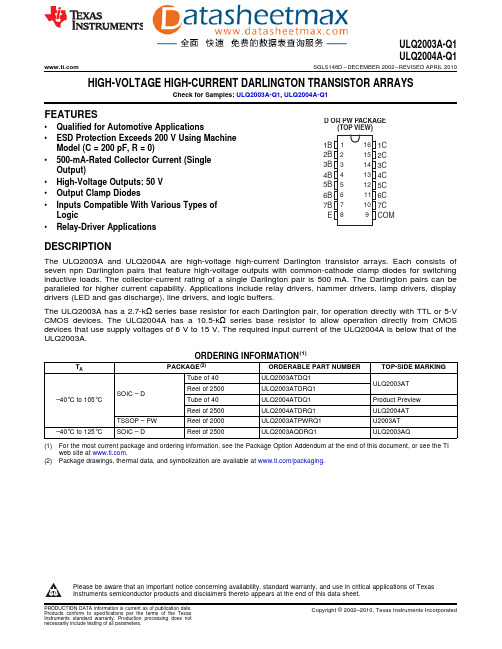
D OR PW PACKAGE(TOP VIEW)1B 1162B 2153B 3144B 4135B 5126B 6117B 710E891C 2C 3C 4C 5C 6C 7C COMULQ2003A-Q1ULQ2004A-Q1SGLS148D –DECEMBER 2002–REVISED APRIL 2010HIGH-VOLTAGE HIGH-CURRENT DARLINGTON TRANSISTOR ARRAYSCheck for Samples:ULQ2003A-Q1,ULQ2004A-Q1FEATURES•Qualified for Automotive Applications•ESD Protection Exceeds 200V Using Machine Model (C =200pF,R =0)•500-mA-Rated Collector Current (Single Output)•High-Voltage Outputs:50V •Output Clamp Diodes•Inputs Compatible With Various Types of Logic•Relay-Driver ApplicationsDESCRIPTIONThe ULQ2003A and ULQ2004A are high-voltage high-current Darlington transistor arrays.Each consists of seven npn Darlington pairs that feature high-voltage outputs with common-cathode clamp diodes for switching inductive loads.The collector-current rating of a single Darlington pair is 500mA.The Darlington pairs can be paralleled for higher current capability.Applications include relay drivers,hammer drivers,lamp drivers,display drivers (LED and gas discharge),line drivers,and logic buffers.The ULQ2003A has a 2.7-k Ωseries base resistor for each Darlington pair,for operation directly with TTL or 5-V CMOS devices.The ULQ2004A has a 10.5-k Ωseries base resistor to allow operation directly from CMOS devices that use supply voltages of 6V to 15V.The required input current of the ULQ2004A is below that of the ULQ2003A.ORDERING INFORMATION (1)T APACKAGE (2)ORDERABLE PART NUMBER TOP-SIDE MARKING Tube of 40ULQ2003ATDQ1ULQ2003AT Reel of 2500ULQ2003ATDRQ1SOIC –D–40°C to 105°CTube of 40ULQ2004ATDQ1Product Preview Reel of 2500ULQ2004ATDRQ1ULQ2004AT TSSOP –PWReel of 2000ULQ2003ATPWRQ1U2003AT –40°C to 125°C SOIC –DReel of 2500ULQ2003AQDRQ1ULQ2003AQ(1)For the most current package and ordering information,see the Package Option Addendum at the end of this document,or see the TI web site at .(2)Package drawings,thermal data,and symbolization are available at /packaging .Please be aware that an important notice concerning availability,standard warranty,and use in critical applications of Texas Instruments semiconductor products and disclaimers thereto appears at the end of this data sheet.7C 6C 5C 4C 3C 2C 1CCOM7B6B5B4B3B2B1BULQ2003A:R = 2.7 k B W ULQ2004A:R = 10.5 k B ULQ2003A-Q1ULQ2004A-Q1SGLS148D –DECEMBER 2002–REVISED APRIL 2010LOGIC DIAGRAMSCHEMATICS (EACH DARLINGTON PAIR)A.All resistor values shown are nominal.B.The collector-emitter diode is a parasitic structure and should not be used to conduct current.If the collector(s)go below ground an external Schottky diode should be added to clamp negative undershoots.2Submit Documentation Feedback Copyright ©2002–2010,Texas Instruments IncorporatedULQ2003A-Q1ULQ2004A-Q1 SGLS148D–DECEMBER2002–REVISED APRIL2010 ABSOLUTE MAXIMUM RATINGS(1)at25°C free-air temperature(unless otherwise noted)MIN MAX UNITV CC Collector-emitter voltage50V Clamp diode reverse voltage(2)50VV I Input voltage(2)30V Peak collector current See Figure14500mAI OK Output clamp current500mATotal emitter-terminal current–2.5ASee DissipationP D Continuous total power dissipationRatings TableULQ200xAT–40105T A Operating free-air temperature range°CULQ200xAQ–40125D package73q JA Package thermal impedance(3)(4)°C/WPW package108T stg Storage temperature range–65150°C (1)Stresses beyond those listed under"absolute maximum ratings"may cause permanent damage to the device.These are stress ratingsonly,and functional operation of the device at these or any other conditions beyond those indicated under"recommended operating conditions"is not implied.Exposure to absolute-maximum-rated conditions for extended periods may affect device reliability.(2)All voltage values are with respect to the emitter/substrate terminal E,unless otherwise noted.(3)Maximum power dissipation is a function of T J(max),q JA,and T A.The maximum allowable power dissipation at any allowable ambienttemperature is P D=(T J(max)–T A)/q JA.Operating at the absolute maximum T J of150°C can affect reliability.(4)The package thermal impedance is calculated in accordance with JESD51-7.DISSIPATION RATINGSDERATINGT A=25°CFACTOR T A=85°C T A=105°C T A=125°C PACKAGE POWERABOVE POWER RATING POWER RATING POWER RATINGRATINGT A=25°CD950mW7.6mW/°C494mW342mW190mW Copyright©2002–2010,Texas Instruments Incorporated Submit Documentation Feedback3ULQ2003A-Q1ULQ2004A-Q1SGLS148D –DECEMBER 2002–REVISED APRIL 2010ELECTRICAL CHARACTERISTICSover recommended operating conditions (unless otherwise noted)ULQ2003AT ULQ2003AQ ULQ2004AT TEST PARAMETERTEST CONDITIONSUNITFIGUREMINTYP MAXMINTYP MAXMINTYP MAXI C =125mA 5I C =200mA2.7 2.76I C =250mA 2.92.9On-state input V I(on)Figure 6V CE =2VV voltageI C =275mA 7I C =300mA 33I C =350mA8I I =250m A,I C =100mA 0.9 1.21 1.30.9 1.1Collector-emitter V CE(sat)saturation Figure 5I I =350m A,I C =200mA 1 1.41 1.51 1.3VvoltageI I =500m A,I C =350mA1.21.7 1.21.8 1.21.6T A =25°C 10010050V CE =50V,Figure 1I I =0T A =105°C 165Collector cutoff I CEXm A currentI I =0100Figure 2V CE =50V V I =1V500Clamp forward V F Figure 8I F =350mA1.72.21.72.21.72.1V voltage Off-state input I I(off)Figure 3V CE =50V,I C =500m A 306530655065m Acurrent V I =3.85V0.931.350.931.35I IInput current Figure 4V I =5V 0.350.5mAV I =12V11.45T A =25°C10010050Clamp reverse I R Figure 7V R =50V m A current 100100100InputC iV I =0,f =1MHz152515251525pF capacitanceSWITCHING CHARACTERISTICSover recommended operating conditions (unless otherwise noted)ULQ2003A,ULQ2004APARAMETERTEST CONDITIONSUNIT MINTYP MAX t PLH Propagation delay time,low-to high-level output See Figure 9110m s t PHL Propagation delay time,high-to low-level output See Figure 9110m s V S –V OHHigh-level output voltage after switchingV S =50V,I O =300mA,See Figure 10mV5004Submit Documentation Feedback Copyright ©2002–2010,Texas Instruments IncorporatedOpenOpenOpenV IOpenOpenVIOpenI COpenI CI IOpenI CIFV RULQ2003A-Q1ULQ2004A-Q1SGLS148D –DECEMBER 2002–REVISED APRIL 2010PARAMETER MEASUREMENT INFORMATIONFigure 1.I CEX Test CircuitFigure 2.I CEX Test CircuitFigure 3.I I(off)Test CircuitFigure 4.I I Test CircuitC.I I is fixed for measuring V CE(sat),variable for measuring h FE .Figure 5.h FE ,V CE(sat)Test CircuitFigure 6.V I(on)Test CircuitFigure 7.I R Test Circuit Figure 8.V F Test CircuitFigure 9.Propagation Delay-Time WaveformsCopyright ©2002–2010,Texas Instruments Incorporated Submit Documentation Feedback 5V IH(see Note C)0V V OHV OLOutputVOLTAGEWAVEFORMSULQ2003A-Q1ULQ2004A-Q1SGLS148D –DECEMBER 2002–REVISED APRIL 2010PARAMETER MEASUREMENT INFORMATION (continued)A.The pulse generator has the following characteristics:PRR =12.5kHz,Z O =50Ω.B.C L includes probe and jig capacitance.C.For testing the ULQ2003A,V IH =3V;for the ULQ2004A,V IH =8V.Figure tch-Up Test Circuit and Voltage Waveforms6Submit Documentation Feedback Copyright ©2002–2010,Texas Instruments Incorporated0I C -Collector Current -mA 2.58001002003004005006007000.511.52V C E (s a t )-C o l l e c t o r -E m i t t e r S a t u r a t i o n V o l t a g e -V V C E (s a t )21.510.570060050040030020010008002.5I C(tot)-Total Collector Current -mA0V CE (s a t )-C o l l e c t o r -E m i t t e r S a t u r a t i o n V o l t a g e -VC E (s a t )0I I -Input Current -µA500200025507510012515017550100150200250300350400450I C -C o l l e c t o r C u r r e n t -m AC 0Duty Cycle -%6001000102030405060708090100200300400500C -M a x i m u m C o l l e c t o r C u r r e n t -m AC I ULQ2003A-Q1ULQ2004A-Q1SGLS148D –DECEMBER 2002–REVISED APRIL 2010TYPICAL CHARACTERISTICSCOLLECTOR-EMITTER SATURATION VOLTAGECOLLECTOR-EMITTER SATURATION VOLTAGEvsvsTOTAL COLLECTOR CURRENT (TWO DARLINGTONS INCOLLECTOR CURRENT (ONE DARLINGTON)PARALLEL)Figure 11.Figure 12.D PACKAGECOLLECTOR CURRENTMAXIMUM COLLECTOR CURRENTvsvsINPUT CURRENTDUTY CYCLEFigure 13.Figure 14.Copyright ©2002–2010,Texas Instruments Incorporated Submit Documentation Feedback 7VVULQ2004A ULQ2003ALam TestV VV VULQ2003A-Q1ULQ2004A-Q1SGLS148D –DECEMBER 2002–REVISED APRIL 2010APPLICATION INFORMATIONFigure 15.TTL to LoadFigure 16.Buffer for Higher Current LoadsFigure e of Pullup Resistors to Increase Drive Current8Submit Documentation Feedback Copyright ©2002–2010,Texas Instruments IncorporatedPACKAGING INFORMATIONOrderable Device Status(1)PackageType PackageDrawingPins PackageQtyEco Plan(2)Lead/Ball Finish MSL Peak Temp(3)ULQ2003AQDRQ1ACTIVE SOIC D162500Green(RoHS&no Sb/Br)CU NIPDAU Level-1-260C-UNLIMULQ2003ATDG4Q1ACTIVE SOIC D1640Green(RoHS&no Sb/Br)CU NIPDAU Level-1-260C-UNLIMULQ2003ATDQ1ACTIVE SOIC D1640Green(RoHS&no Sb/Br)CU NIPDAU Level-1-260C-UNLIMULQ2003ATDRG4Q1ACTIVE SOIC D162500Green(RoHS&no Sb/Br)CU NIPDAU Level-1-260C-UNLIMULQ2003ATDRQ1ACTIVE SOIC D162500Green(RoHS&no Sb/Br)CU NIPDAU Level-1-260C-UNLIMULQ2003ATPWRQ1ACTIVE TSSOP PW162500Green(RoHS&no Sb/Br)CU NIPDAU Level-1-260C-UNLIMULQ2004ATDRG4Q1ACTIVE SOIC D162500Green(RoHS&no Sb/Br)CU NIPDAU Level-1-260C-UNLIMULQ2004ATDRQ1ACTIVE SOIC D162500Green(RoHS&no Sb/Br)CU NIPDAU Level-1-260C-UNLIM(1)The marketing status values are defined as follows:ACTIVE:Product device recommended for new designs.LIFEBUY:TI has announced that the device will be discontinued,and a lifetime-buy period is in effect.NRND:Not recommended for new designs.Device is in production to support existing customers,but TI does not recommend using this part in a new design.PREVIEW:Device has been announced but is not in production.Samples may or may not be available.OBSOLETE:TI has discontinued the production of the device.(2)Eco Plan-The planned eco-friendly classification:Pb-Free(RoHS),Pb-Free(RoHS Exempt),or Green(RoHS&no Sb/Br)-please check /productcontent for the latest availability information and additional product content details.TBD:The Pb-Free/Green conversion plan has not been defined.Pb-Free(RoHS):TI's terms"Lead-Free"or"Pb-Free"mean semiconductor products that are compatible with the current RoHS requirements for all6substances,including the requirement that lead not exceed0.1%by weight in homogeneous materials.Where designed to be soldered at high temperatures,TI Pb-Free products are suitable for use in specified lead-free processes.Pb-Free(RoHS Exempt):This component has a RoHS exemption for either1)lead-based flip-chip solder bumps used between the die and package,or2)lead-based die adhesive used between the die and leadframe.The component is otherwise considered Pb-Free(RoHS compatible)as defined above.Green(RoHS&no Sb/Br):TI defines"Green"to mean Pb-Free(RoHS compatible),and free of Bromine(Br)and Antimony(Sb)based flame retardants(Br or Sb do not exceed0.1%by weight in homogeneous material)(3)MSL,Peak Temp.--The Moisture Sensitivity Level rating according to the JEDEC industry standard classifications,and peak solder temperature.Important Information and Disclaimer:The information provided on this page represents TI's knowledge and belief as of the date that it is provided.TI bases its knowledge and belief on information provided by third parties,and makes no representation or warranty as to the accuracy of such information.Efforts are underway to better integrate information from third parties.TI has taken and continues to take reasonable steps to provide representative and accurate information but may not have conducted destructive testing or chemical analysis on incoming materials and chemicals.TI and TI suppliers consider certain information to be proprietary,and thus CAS numbers and other limited information may not be available for release.In no event shall TI's liability arising out of such information exceed the total purchase price of the TI part(s)at issue in this document sold by TI to Customer on an annual basis.OTHER QUALIFIED VERSIONS OF ULQ2003A-Q1,ULQ2004A-Q1:•Catalog:ULQ2003A,ULQ2004ANOTE:Qualified Version Definitions:•Catalog-TI's standard catalog productTAPE AND REEL INFORMATION*All dimensions are nominal Device Package Type Package DrawingPinsSPQ Reel Diameter (mm)Reel Width W1(mm)A0(mm)B0(mm)K0(mm)P1(mm)W (mm)Pin1Quadrant ULQ2003ATPWRQ1TSSOP PW 162500330.012.4 6.9 5.6 1.68.012.0Q1*All dimensions are nominalDevice Package Type Package Drawing Pins SPQ Length(mm)Width(mm)Height(mm)ULQ2003ATPWRQ1TSSOP PW162500346.0346.029.0IMPORTANT NOTICETexas Instruments Incorporated and its subsidiaries(TI)reserve the right to make corrections,modifications,enhancements,improvements, and other changes to its products and services at any time and to discontinue any product or service without notice.Customers should obtain the latest relevant information before placing orders and should verify that such information is current and complete.All products are sold subject to TI’s terms and conditions of sale supplied at the time of order acknowledgment.TI warrants performance of its hardware products to the specifications applicable at the time of sale in accordance with TI’s standard warranty.Testing and other quality control techniques are used to the extent TI deems necessary to support this warranty.Except where mandated by government requirements,testing of all parameters of each product is not necessarily performed.TI assumes no liability for applications assistance or customer product design.Customers are responsible for their products and applications using TI components.To minimize the risks associated with customer products and applications,customers should provide adequate design and operating safeguards.TI does not warrant or represent that any license,either express or implied,is granted under any TI patent right,copyright,mask work right, or other TI intellectual property right relating to any combination,machine,or process in which TI products or services are rmation published by TI regarding third-party products or services does not constitute a license from TI to use such products or services or a warranty or endorsement e of such information may require a license from a third party under the patents or other intellectual property of the third party,or a license from TI under the patents or other intellectual property of TI.Reproduction of TI information in TI data books or data sheets is permissible only if reproduction is without alteration and is accompanied by all associated warranties,conditions,limitations,and notices.Reproduction of this information with alteration is an unfair and deceptive business practice.TI is not responsible or liable for such altered rmation of third parties may be subject to additional restrictions.Resale of TI products or services with statements different from or beyond the parameters stated by TI for that product or service voids all express and any implied warranties for the associated TI product or service and is an unfair and deceptive business practice.TI is not responsible or liable for any such statements.TI products are not authorized for use in safety-critical applications(such as life support)where a failure of the TI product would reasonably be expected to cause severe personal injury or death,unless officers of the parties have executed an agreement specifically governing such use.Buyers represent that they have all necessary expertise in the safety and regulatory ramifications of their applications,and acknowledge and agree that they are solely responsible for all legal,regulatory and safety-related requirements concerning their products and any use of TI products in such safety-critical applications,notwithstanding any applications-related information or support that may be provided by TI.Further,Buyers must fully indemnify TI and its representatives against any damages arising out of the use of TI products in such safety-critical applications.TI products are neither designed nor intended for use in military/aerospace applications or environments unless the TI products are specifically designated by TI as military-grade or"enhanced plastic."Only products designated by TI as military-grade meet military specifications.Buyers acknowledge and agree that any such use of TI products which TI has not designated as military-grade is solely at the Buyer's risk,and that they are solely responsible for compliance with all legal and regulatory requirements in connection with such use. TI products are neither designed nor intended for use in automotive applications or environments unless the specific TI products are designated by TI as compliant with ISO/TS16949requirements.Buyers acknowledge and agree that,if they use any non-designated products in automotive applications,TI will not be responsible for any failure to meet such requirements.Following are URLs where you can obtain information on other Texas Instruments products and application solutions:Products ApplicationsAmplifiers Audio /audioData Converters Automotive /automotiveDLP®Products Communications and /communicationsTelecomDSP Computers and /computersPeripheralsClocks and Timers /clocks Consumer Electronics /consumer-appsInterface Energy /energyLogic Industrial /industrialPower Mgmt Medical /medicalMicrocontrollers Security /securityRFID Space,Avionics&/space-avionics-defenseDefenseRF/IF and ZigBee®Solutions /lprf Video and Imaging /videoWireless /wireless-appsMailing Address:Texas Instruments,Post Office Box655303,Dallas,Texas75265Copyright©2010,Texas Instruments Incorporated。
MatchmakerGoldYe...

MatchmakerGoldYe...United States/Canada 800.662.2566Asia Paci?c+1.650.919.7300Europe+33.(0)1.3904.6880Japan+81.(0)77.543.6116Clontech Laboratories, Inc.A T akara Bio Company 1290 T erra Bella Ave.Mountain View, CA 94043C e r t i ?c a t e o f A n a l y s i sDESCRIPTIONA simple and highly efficient system for the simultaneous construction and screening of a cDNA library for protein-DNA interactions. SMART? cDNA is synthesized from your RNA sample and then used to construct a library directly in a Y1HGold yeast reporter strain containing your DNA sequence of interest. Positive protein-DNA interactions from the library convey resistance to the yeast antibiotic, Aureobasidin A (AbA).Box 3:Yeastmaker ? Y east T ransformation System 2 (Box 2 of 2) –2 x 50 ml 50% PEG – 50 ml 1 M LiAc (10X) – 50 ml 10X T E Buffer – 50 ml YPD Plus Liquid Medium Box 4:10 μl SMART? III Oligonucleotide (12 μM)? 5 μl Control PolyA + RNA(Human Placenta; 1 μg/μl)0.5 ml S. cerevisiae Y 1HGold Box 5:1 pouch YPDA Broth (0.5 L)? 1 pouch YPDA with Agar (0.5 L)?1 pouch SD/-Ura with Agar (0.5 L)? 50 ml NaCl Solution (0.9%)? 300 μl Sodium Acetate (3 M)? 500 μl Deionized H 2O ? 10 ea CHROMA SPIN TM +TE-400ColumnsOTHERMatchmaker Gold Yeast One-Hybrid Library Screening System User Manual (PT4087-1)Yeastmaker Yeast Transformation System 2 User Manual (PT1172-1)? pGADT7-Rec Vector Information (PT3530-5) pAbAi Vector Information (PT4091-5)pGADT7 AD Vector Information (PT3249-5)PRODUCT : Matchmaker? Gold Y east One-Hybrid Library Screening SystemCATALOG No: 630491LOT NUMBER:Specified on product label.AMOUNT : 5 reactionsSTORAGE CONDITIONS: See page 2SHELF LIFE: See page 2 SHIPPING CONDITIONS: See page 2PACKAGE CONTENTS Box 1:10 μl SMART? MMLV RT(200 units/μl; also available as Cat. No. 639522)300 μl 5X First-Strand Buffer ? 165 μl DTT (100 mM)10 μl CDS III Primer (12 μM)? 10 μl CDS III/6 Primer (10 μM)?50 μl 5' PCR Primer (10 μM)? 50 μl 3' PCR Primer (10 μM)? 7 μl RNaseH (2 units/μl)? 500 μl Melting Solution50 μl dNTP Mix (10 mM each dNTP)? 25 μg pGADT7-Rec AD Cloning Vector(SmaI-linearized; 500 ng/μl)20 μg pAbAi Vector (500 ng/μl)? 10 μg p53-AbAi Control Vector(500 ng/μl)625 ng p53 Control Insert (25 ng/μl)? 50 μl pGADT7 AD Vector (100 ng/μl)Box 2:Yeastmaker ? Y east T ransformation System 2 (Box 1 of 2): – 2 x 1 ml Yeastmaker Carrier DNA,denatured (10 mg/ml)–20 μl pGBT9 (0.1 μg/μl;control plasmid)APPROVED BY: _________________________(PA913047)FOR RESEARCH USE ONL YQUALITY CONTROL DATA See page 2.In the interest of conserving resources, we are no longer shipping manuals with products. Please visit /doc/a218592079.html,/manuals to obtain an electronic version.STORAGE CONDITIONSStore Boxes 1 & 2 at –20°C.Store Box 4 at –70°C.Store Boxes 3 & 5 at room temperature.SHELF LIFE:1 year from date of receipt under proper storage conditions.SHIPPING CONDITIONSBoxes 1, 2 & 4: Dry ice (–70°C)Boxes 3 & 5: Room temperatureQUALITY CONTROL DATA1.Plasmid Identity and PurityA. The identity of the included vectors were verified by agarose/EtBr gel electrophoresis afterdigestion with the indicated enzymes. The purity of each vector was checked by determining the A260/A280.Vector Enzyme(s) Fragment Size (kb)pGADT7-Rec SmaI 8.0pAbAi BstBI 4.9BbsI 4.9HindIII/PvuII 3.0, 1.8p53-AbAi BstBI 4.9BamHI 4.6, 0.3pGADT7 AD EcoRI 8.0HindIII 7.2, 0.8A260/A280: 1.8–2.0B. The pGADT7-Rec AD Cloning Vector (SmaI-linearized) was also checked by transformation intoFusion-Blue? competent E. coli (Cat. No. 636700). Transformants were selected by plating on LB/ Amp (100 μg/ml). The linearized vector produced ≤ 0.5% of the number of colonies produced with circular (uncut) pGADT7-Rec.2.Y east StrainThe nutritional requirements (auxotrophic markers) of the Y1HGold strain were verified by streaking samples onto several types of SD minimal media.3.cDNA Synthesis & Recombination-mediated CloningA.Single-stranded cDNA was generated from 1 μg of Control Human Placenta Poly A+ RNA usingSMART?MMLV Reverse Transcriptase as described in the User Manual (PT4087-1). Two samples of first-strand cDNA were prepared: One was generated with the CDS III Primer; the other, with the CDS III/6 Primer. Next, 2 μl of eac h cDNA sample was amplified by PCR, to prepare ds cDNA as described in the User Manual. Finally, 5 μl of the PCR product was electrophoresed on a 1.2% agarose/EtBr gel. A moderately strong smear from ≥0.1 kb to 4 kb (or more) was observed.3.cDNA Synthesis & Recombination-mediated Cloning (cont'd)B. Recombination-mediated cloning was tested with the following four transformations:Competent ds cDNA pGADT7-Rec T ransformation Y1HGold[p53-AbAi] cells CDS III a CDS III/6a p53b Blank c(SmaI-linearized)1. 100 μl 5 μl ———1 μg2. 100 μl —5 μl ——1 μg3. 100 μl ——5 μl—1 μg4. 100 μl ———5 μl 1 μga First-strand cDNA was synthesized as in Part 3a, above, using either the CDS III or CDS III/6 Primer. T he cDNA was then PCRamplified, purified by gel filtration (using a CHROMA SPIN+TE-400 Column, Cat. No. 636076), and finally, concentrated by ethanol precipitation, all as described in PT4087-1.b p53 Control Insertc The Blank was prepared and processed in the same way as the CDS III and CDS III/6 samples with one exception: HumanPlacenta Poly A+ RNA was omitted from the first-strand synthesis reaction.Following transformation, the mixtures were spread on SD/–Leu agar medium and incubated at 30°C. T ransformation #4, a negative control, produced ≤20% of t he number of colonies observed for Transformations #1 or #2.C. Detection of the yeast one-hybrid interaction between p53 and the p53 cis-DNA consensus bindingelementTransformation #3, in Part 3B above, yielded transformants when plated on SD/-Leu agar + 200 ng/ml Aureobasidin A , while Y1HGold[p53-AbAi] transformed with the pGADT7-Rec Vectoralone (circular) gave less than 2% of the number of colonies obtained for T ransformation #3 on the SD/-Leu agar + 200 ng/ml Aureobasidin A.Notice to PurchaserClontech products are to be used for research purposes only. They may not be used for any other purpose, including, but not limited to, use in drugs, in vitro diagnostic purposes, therapeutics, or in humans. Clontech products may not be transferred to third parties, resold, modified for resale, or used to manufacture commercial products or to provide a service to third parties without written approval of Clontech Laboratories, Inc.SMART? Amplification Products:SMART Amplification Products are covered by U.S. Patent Nos. 5,962,271 and 5,962,272. For-Profit and Not-For-Profit purchasers of SMART Amplification Products are entitled to use the reagents for internal research. However, the following uses are expressly pro-hibited: (1) performing services for third parties;(2) identifying nucleic acid sequences to be included on nucleic acid arrays, blots, or in libraries or other cDNA collections which are then sold to third parties. Reproduction, modification, reformulation, or resale of the reagents provided in SMART Amplification Products is not permitted. For information on licensing SMART T echnology for commercial purposes, please contact a licensing representative by phone at 650.919.7320 or by e-mail at licensing@/doc/a218592079.html,. Aureobasidin A Resistance Gene:This product is covered by the claims of U.S. Patent No. 6,015,689 and its foreign counterpart patent claims owned by Takara Bio Inc. Rights to use this product are limited to research only. Use of this product for purposes other than research mayrequire a license, and inquiry concerning such commercial use should be directed to T akara Bio Inc., Seta 3-4-1, Otsu, Shiga 520-2193, Japan.Clontech, the Clontech Logo and all other trademarks are property of Clontech Laboratories, Inc. unless noted otherwise.Clontech is a T akara Bio Company. ?2009 Clontech Laboratories, Inc.。
- 1、下载文档前请自行甄别文档内容的完整性,平台不提供额外的编辑、内容补充、找答案等附加服务。
- 2、"仅部分预览"的文档,不可在线预览部分如存在完整性等问题,可反馈申请退款(可完整预览的文档不适用该条件!)。
- 3、如文档侵犯您的权益,请联系客服反馈,我们会尽快为您处理(人工客服工作时间:9:00-18:30)。
c) x(0) = 2
Ici C = 4. Il faut donc que sin 2t + 4 > 0 ou encore t ∈ R. L'intervalle maximal de dénition est R.
d) x(π) = 1
Ici C = 1. Il faut donc que sin 2t + 1 > 0 ou encore
..
.
e−λn t
· H · B (t)
ou encore
V (t) = G
λ1 eλ1 t
..
.λn eλn t (t) + GHB (t)
D'autre part
AV (t) + B (t) = AG
eλ1 t
..
.
eλ n t
I (t) + B (t)
xdx = cos 2t dt
En intégrant cette équation à variables séparées, on trouve
sin 2t x2 = +K 2 2
avec K une constante. Posant 2K = C , on obtient
x(t)2 = sin 2t + C
I =] − π/12, 7π/12[
b) x(0) = 1
Ici C = 1. Il faut donc que sin 2t + 1 > 0 ou encore
t∈ ] − π/4 + kπ, 3π/4 + kπ [
k ∈Z
L'intervalle maximal de dénition est le plus grand sous-intervalle de cet ensemble contenant 0. L'intervalle cherché est alors
telles que ...
e−λn u · H · B (u)du
...
t
0
e−λ1 u
eλn t
·
On peut trouver les conditions qu'il faut imposer à G, H an que la fonction V proposée soit solution du problème de Cauchy. D'abord il est évident que V (0) = 0, car pour t = 0, l'intégrale est nulle. Il reste à comprendre à quelle condition cette fonction V est solution de
V = AV + B (t)
Notons
t
I (t) =
0
e−λ1 u
..
.
e−λn u
· H · B (u)du
Alors
V (t) = G λ1 eλ1 t
..
eλ1 t
.
λn eλn t
I (t) + G
..
e−λ1 t
.
eλn t
Q2. Donner, pour chacune des conditions initiales ci-dessous, l'intervalle de dénition de la solution maximale associée. Dessiner également les graphes de ces solutions maximales. 1 a) x(0) = √ . 2
avec k, l, m, n 4 constantes réelles quelconques.
Equation II : linéaire non homogène
On considère une matrice complexe A de taille n × n. On suppose que son polynôme caractéristique possède n racines distinctes complexes, c'est-à-dire Soit B : R → M (C) une fonction continue à valeurs dans l'espace vectoriel complexe des matrices-colonne ayant n lignes. On appelle V : R → M (C) l'unique solution du problème de Cauchy formé par l'équation diérentielle linéaire non homogène et la condition initiale ci-dessous :
x =
pour établir l'existence des deux matrices G, H .
On s'intéresse aux solutions maximales de l'équation diérentielle
cos 2t x U = {(t, x) ∈ R2 , x > 0}
Équations diérentielles 1. *** Corrigé ***
Quatre équations diérentielles
1 0 0 0 0 −1 −1 1 1 1 V = 0 −2 −2 −1 1 1 0 −k k 0)
dont les solutions sont de la forme
V = t (k
L'espace propre de 1 est alors seulement de dimension 1. La matrice n'est pas diagonalisable. Les solutions sont alors de la forme
1 0 0 0 0 −1 −1 1 1 1 A = t (k − k k 0) −2 −2 −1 1 1 1 0 A1 = t ( l −l l − k)
Le résultat est Ensuite, V2 est solution de
(M − 2I )V2 = 0
n,1 n,1
Spec(A) = {λ1 , · · · , λn } ⊂ C
∀t ∈ R,
V (t) = A · V (t) + B (t) V (0) = 0
n,n (C)
Démontrer qu'il existe deux matrices constantes G, H ∈ M
∀t ∈ R, V (t) = G · eλ1 t
t∈ ] − π/4 + kπ, 3π/4 + kπ [
k ∈Z
L'intervalle maximal de dénition est le plus grand sous-intervalle de cet ensemble contenant π . L'intervalle cherché est alors
H = G−1
Equation III : non-linéaire du premier ordre
dont les graphes sont contenus dans le demi-plan ouvert Q1. Trouver une équation reliant x(t) et t.
Ici 1/2 = C . Il faut donc que sin 2t + (1/2) > 0 ou encore
2t ∈
k∈Z
] − π/6 + 2kπ, 7π/6 + 2kπ [
ce qui équivaut à
t∈ ] − π/12 + kπ, 7π/12 + kπ [
k ∈Z
L'intervalle maximal de dénition est le plus grand sous-intervalle de cet ensemble contenant 0. L'intervalle cherché est alors
λ1
..
.
λn
−1 = G AG
Or comme A est diagonalisable, et de spectre {λ1 , . . . , λn }, il existe une matrice G (inversible) telle que G−1 AG soit la matrice de diagonale (λ1 , . . . , λn ). Cette matrice G est une matrice de passage de la base canonique à une base de vecteurs propres de la matrice A (dans l'ordre des valeurs propres λ1 , . . . , λn ). Il sut ensuite de prendre
L'égalité V = AV + B a lieu si on a en même temps
G λ 1 eλ 1 t = = AG In