DC232007 RPR技术 ISSUE1.00
AnaChip AP2007 数据手册
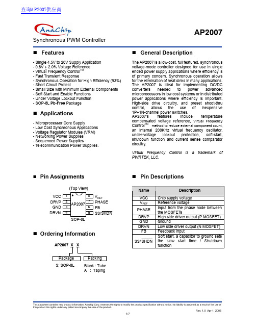
AP2007Synchronous PWM ControllerFeatures- Single 4.5V to 20V Supply Application - 0.8V + 2.0% Voltage Reference - Virtual Frequency Control TM - Fast Transient Response- Synchronous Operation for High Efficiency (93%) - Short Circuit Protect- Small Size with Minimum External Components - Soft Start and Enable Functions - Under Voltage Lockout Function - SOP-8L Pb-Free PackageApplications- Microprocessor Core Supply- Low Cost Synchronous Applications - Voltage Regulator Modules (VRM) - Networking Power Supplies - Sequenced Power Supplies- Telecommunication Power Supplies.General DescriptionThe AP2007 is a low-cost, full featured, synchronous voltage-mode controller designed for use in single ended power supply applications where efficiency is of primary concern. Synchronous operation allows for the elimination of heat sinks in many applications. The AP2007 is ideal for implementing DC/DC converters needed to power advanced microprocessors in low cost systems or in distributed power applications where efficiency is important. High-side drive circuitry, and preset shoot-thru control, allows the use of inexpensive 1P+1N-channel power switches.AP2007’s features include temperature compensated voltage reference, Virtual Frequency Control TM method to reduce external component count, an internal 200KHz virtual frequency oscillator, under-voltage lockout protection, soft-start, shutdown function and current sense comparator circuitry.Virtual Frequency Control is a trademark of PWRTEK, LLC.Pin AssignmentsSOP-8L1(Top View)VCC V REFPHASE DRVP DRVNFBGND AP20072345678SS/SHDNOrdering InformationAP2007 X X Package Packing S: SOP-8LBlank : Tube A : TapingPin DescriptionsNameDescriptionVCC Chip supply voltage V REF Reference voltagePHASEInput from the phase node betweenthe MOSFET sDRVP High side driver output (P MOSFET)GND Ground DRVN Low side driver output (N MOSFET) FB Feedback inputSS/SHDN Soft start, a capacitor to ground setsthe slow start time / Shutdownfunction查询AP2007供应商Synchronous PWM ControllerBlock DiagramCROSS CURRENT CONTROL DRVNVIRTUAL FREQ OSCILLATORDRVPR Q SQSQB R+-+-+-+-VOLTAGE REFERENCE +-VCC0.8VUNDER VOLTAGEERROR COMPVCC 12ua2ua0.2V0.9VSS/SHDNFBGNDOCSETPHASEVCCDRVPDRVNAP2007 FUNCTIONAL BLOCK DIAGRAMVirtual Frequency Control - PatentNumber 6,456,050.V REF-+0.4V -+0.4VAbsolute Maximum RatingsSymbol ParameterRange. Unit V IN VCC to GND -1 to 22 V V PHASE PHASE to GND -1 to 22 V V DRVP DRVP to GND -1 to 22 V V DRVN DRVN to GND-1 to 22 V θJC Thermal Resistance Junction to Case 90 oC/W θJA Thermal Resistance Junction to Ambient 250 oC/W T OP Operating Temperature Range -40 to +85 o C T ST Storage Temperature Range-65 to +150o C T LEADLead Temperature (Soldering) 10 Sec.300o CSynchronous PWM ControllerElectrical CharacteristicsUnless specified: V CC =12V; GND = 0V;V O = 5V; T J = 25oCSymbol Parameter Conditions Min. Typ. Max. Unit Power SupplyV CC Supply Voltage(Recommended)4.5 - 20 VI CC Supply Current DRVP & DRVN are floating - 9.5 - mA ∆V LINE Line Regulation V O = 2.5V - 0.5 % Error Comparator A OL Gain (A OL ) - 70 - dB I B Input Bias - 0.2 1 uA Oscillator F OSC Oscillator Frequency - 200 - KHz DC MAX Oscillator Max Duty Cycle 80 85 - % Mofset DriversI DRVP DRVP Source/Sink V CC – V DRVP =3VV DRVP – V GND = 2V 0.5 1 - AI DRVN DRVN Source/Sink V CC – V DRVN = 3VV DRVL – V GND = 2V0.5 1 - AV DRVL DRVP/N Low Level Voltage - - 1.2 V V DRVH DRVP/N High Level Voltage V CC -1.2- - V ProtectionT DEAD Dead Time DRVP & DRVN are floating - 150 - nS Vocset Over Current Setting Voltage 0.4 VV DRVP/N DRVP/DRVN System ErrorVoltage (Note3) V SS =Low, V CC <3.8, over current happenV CC -1.2- - VReferenceReference Voltage 0.7840.8 0.816V V REF Accuracy 0o C to 70oC-2 - + 2 %Soft StartI SSC Charge Current V SS = 1.5V 8.0 10 12 uA I SSD Discharge Current V SS = 1.5V 1.3 2 2.7 uA Under voltage lockout (UVLO)V UT Upper Threshold Voltage (V CC )- 4.0 - V V LWT Lower Threshold Voltage (V CC )- 3.8 - V V HT Hysteresis (V CC ) - 200 - mVNote 1. Specification refers to Typical Application Circuit.Note 2. This device is ESD sensitive. Use of standard ESD handling precautions is required. Note 3. Abnormal condition; Ex: over-current, under-voltage lockout, soft-start disappear.Synchronous PWM ControllerTypical Application Circuit87651234D1Option VCC SS/SHDN FB DRVP GNDPHASE DRVN Q1Q2L110uHC8470u/16V C9Vout=3.2V*+-+-C1R21KR33K ** Vout = 0.8 x (1+R3/R2)AP2007C4330nC3330nR112ΩV REF 10n470u/16V470u/16VAF9435C5AF9410C20.1uC647n C70.1u 1ΩOption 1ΩOptionR2 1K ~ 10K≅(4835)(4412)Virtual Frequency ControlVirtual Frequency Control combines the advantages of constant frequency and constant off-time control in a single mode of operation. This allows fix frequency, precision switching voltage regulator control with fast transient response and the smallest solution size. Switch duty cycle can be adjusted from 0% to 100% on a pulse by pulse basis when responding to transient conditions. Both 0% and 100% duty cycle operation can be maintained for extended periods of time in response to load or line transients. Figure 1 depicts a simplified operation of the Virtual Frequency Controltechnique: The VFC oscillator generates a pulse of a known duration (VFC_Pulse). The regulator loop responds by returning a complementary feedback pulse (FB_Pulse). The FB_Pulse duration is a result of external conditions such as inductor size, the voltage across the inductor and the duration of the VFC_Pulse. A VFC control loop is then formed whereby the duration of the VFC_Pulse is modified as a result of the FB_Pulse duration. The VFC loop arrives at a state of equilibrium, where the operating frequency remains inherently constant.GATE CONTROL LOGICVIRTUAL FREQ OSCILLATOR+-FB PulseVFC PulseVrefERROR COMPV INLout CoutVout Rfb1Rfb2Figure 1: Virtual Frequency Control Loop- Synchronous single supply application.Synchronous PWM with VFC Controller (Preliminary) Virtual Frequency Control (Continued)Virtual frequency control is a technique that provides stable, constant frequency of operation for pulse controlled architectures such as constant off-time/on-time. This is all done internal to the IC with minimal number of components and without the need for connections to external terminals such as input and/or output. No external compensation is required, thus providing a low cost, high performance fix frequency solution for switching voltage regulators.Virtual Frequency Control is a trademark of PWRTEK, LLC.Function DescriptionSynchronous Buck ConverterPrimary V CORE power is provided by a synchronous, voltage-mode pulse width modulated (PWM) controller. This section has all the features required to build a high efficiency synchronous buck converter, including soft-start, shutdown, and cycle-by-cycle current limit.Referring to the functional block diagram FIG 1, the output voltage of the synchronous converter is set and controlled by the output of the error comparator. The external resistive divider reference voltage, is derived from an internal trimmed-bandgap voltage reference. The inverting input of the error comparator receives its voltage from the FB pin.The internal oscillator uses an on-chip capacitor and trimmed precision current sources to set the virtual oscillation frequency to 200KHz. The virtual frequency oscillator sets the PWM latch. This pulls DRVN low, turning off the low-side N_MOSFET and DRVP is pulled low, turning on the high-side P-MOSFET (once the cross-current control allows it). The triangular voltage ramp at the FB pin is then compared against the reference voltage at the inverting input of the error comparator. When the FB voltage increases above the reference voltage, the comparator output goes high. This pulls DRVP high, turning off the high-side P-MOSFET, and DRVN is pulled high, turning on the low-side N-MOSFET (once the cross-current control allows it). The Virtual Frequency Oscillator then generates a programmed off time to allow the FB voltage to return to the valley voltage of the triangular ramp. At the end of the off time the PWM latch is set and the cycle repeats again.Under Voltage LockoutThe under voltage lockout circuit of the AP2007 assures that the high-side P-MOSFET driver outputs remain in the off state whenever the supply voltage drops below set parameters. Lockout occurs if V CC falls below 3.8V. Normal operation resumes once V CC rises above 4.0V. R DS(ON) Current LimitingThe current limit threshold (0.4V) is set by connecting an internal resistor from the V CC supply to OCSET. Vocset is compared to the voltage at the PHASE node. This comparison is made only when the high-side drive is high to avoid false current limit triggering due to uncontributing measurements from the MOSFET s off-voltage. When the voltage at PHASE is less than the voltage at OCSET, an over-current condition occurs and the soft start cycle is initiated. The synchronous switchturns on and SS/SHDN starts to sink 2uA. When SS/ SHDN reaches 0.2V, it then starts to source 10uA and a new cycle begins. When the soft start voltage is below 0.9V the cycle is controlled with pulse by pulse current limiting.Soft StartInitially, SS/SHDN pin sources 10uA of current to charge an external capacitor. The inverting input of the error comparator is clamped to a voltage proportional to the voltage on SS/SHDN. This limits the on-time of the high-side P-MOSFET, thus leading to a controlled ramp-up of the output voltages.Synchronous PWM with VFC Controller (Preliminary)Function Description (Continued)Hiccup ModeDuring power up, the SS/SHDN pin is internally pulled low until V CC reaches the under-voltage lockout level of 4V. Once V CC has reached 4V, the SS/SHDN pin is released and begins to source 10uA of current to the external soft-start capacitor. As the soft-start voltage rises, the inverting input of the error comparator is clamped to this voltage. When the error signal reaches the level of the internal 0.8V reference, the output voltage is to have reached its programmed voltage. If an over-current condition has not occurred the soft-start voltage will continue to rise and level off at about 2.5V.An over-current condition occurs when the high-side drive is turned on, but the PHASE node does not reach the voltage level set at the OCSET pin. Once an over-current occurs, the high-side drive is turned off and the low-side drive turns on and the SS/SHDN pin begins to sink 2uA. The soft-start voltage will begin to decrease as the 2uA of current discharge the external capacitor. When the soft-start voltage reaches 0.2V, the SS/SHDN pin will begin to source 10uA and begin to charge the external capacitor causing the soft-start voltage to rise again. If the over-current condition is no longer present, normal operation will continue. If the over-current condition is still present, the SS/SHDN pin will again begin to sink 2uA. This cycle will continue indefinitely until the over-current condition is removed.In order to prevent substrate glitching, a small-signal diode should be placed in close proximity to the chip with cathode connected to PHASE and anode connected to GND.Marking Information(Top View)SOP-8L184AP2007YY WW XLogo"02" =2002~5Synchronous PWM ControllerPackage InformationPackage Type: SOP-8LVIEW "A"LHECVIEW "A"AA 2A 1B e D7(4X)0.015x457(4X)yDimensions In Millimeters Dimensions In Inches SymbolMin. Nom. Max. Min. Nom. Max.A 1.40 1.60 1.75 0.055 0.063 0.069 A1 0.10 - 0.25 0.040 - 0.100 A2 1.30 1.45 1.50 0.051 0.057 0.059B 0.33 0.41 0.51 0.013 0.016 0.020C 0.19 0.20 0.25 0.0075 0.008 0.010D 4.80 5.05 5.30 0.189 0.199 0.209E 3.70 3.90 4.10 0.146 0.154 0.161 e - 1.27 - - 0.050 - H 5.79 5.99 6.20 0.228 0.236 0.244 L 0.38 0.71 1.27 0.015 0.028 0.050 y - - 0.10 - - 0.004θ0O - 8O 0O- 8O。
BF6910(BF6911)ASXX规格书
3.1 引脚图 ....................................................................................................................................................... 6 3.2 引脚描述 ................................................................................................................................................... 6
Odyssey CLX 操作指南1
导入图片 ........................................................................................................................... 18 泳道设置 ........................................................................................................................... 19 设定 Marker....................................................................................................................... 20 创建新 marker ................................................................................................................... 20 自动识别条带 ................................................................................................................... 21 手动编辑条带 ................................................................................................................... 21 单通道信号归一化 ..............................................................................................................21 查看表格 ........................................................................................................................... 22
pl2303的2007 -回复
pl2303的2007 -回复PL2303的2007年PL2303是一种高集成度的USB转串口芯片,由台湾普元科技(Prolific Technology Inc.)公司设计和生产。
它在2007年的时候,正值其研发和推广的蓬勃发展期。
本文将详细探讨PL2303在2007年的发展及应用情况。
2007年是科技领域发展迅猛的一年,特别是在USB接口和设备市场上。
随着计算机应用日益广泛,用户对于USB接口设备需求的增长推动了PL2303芯片的研发和应用。
PL2303通过将串行通信转换为USB通信的方式,为计算机用户提供了更为便利的外部设备连接方式。
在2007年,随着PL2303芯片的不断改进和升级,其性能和稳定性都得到了显著提升。
相较于其前身PL2301和PL2302,PL2303在传输速率、数据稳定性以及驱动程序的兼容性方面有了更大的突破。
同时,PL2303在使用上也更加便捷,用户只需将其连接到计算机的USB接口上,通过合适的驱动程序即可实现串行通信。
2007年,PL2303的应用领域也不断扩展和深化。
作为一款USB转串口芯片,PL2303在各种嵌入式系统中的应用得到了广泛关注。
通过PL2303芯片,嵌入式系统可以轻松地与电脑建立串行通信,并实现各种数据传输。
这在工业控制、通信设备、车载系统等领域尤为重要。
同时,PL2303还被用于各种计算机外部设备,如打印机、移动电话、摄像机等的通信连接。
PL2303的广泛应用带来了市场的巨大需求,在2007年这一年也取得了相应的成绩。
台湾普元科技公司积极扩大产能和市场影响力,加大了对PL2303的推广力度。
同时,为了提高PL2303的市场占有率,普元科技还提供了优秀的技术支持和售后服务。
这一系列措施使得PL2303在2007年得到了更广泛的认可和应用,为普元科技的业绩增长做出了重要贡献。
不过,2007年也是PL2303面临一些挑战的一年。
与其他类似产品相比,PL2303仍然存在一些竞争压力。
Phoenix与DC-7技术对比表
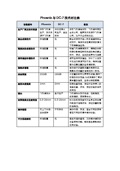
232dB
160dB
大容量的数字化声束形成器,提供了极宽的动态范围,为成像提供了更多更丰富的信息,图像分辨率更高。
最低血流速度
1mm
2mm
拓宽检查范围,保证对各种病人的准备检查、评估,保证设备的临床实用性
探头
飞利浦探头
自行生产
飞利浦探头技术先进、性能稳定,成像清晰、使用寿命长。
取样宽度及位置范围
Phonix
DC-7
备注
生产厂商及技术来源
东软飞利浦生产,技术来源于飞利浦
深圳迈瑞公司生产,自主研发
东软飞利浦是东软、飞利浦共有的合资公司,超声技术来源于飞利浦公司,处于行业领先地位。
融合成像技术
标准配置
无
融合成像技术是一种多通道频率合成技术,确保系统在高帧频的情况下获得最佳图像。
微细灰阶成像技术
标准配置
无
移植飞利浦高端技术,精确的发射和接收聚焦控制和先进的焦点复合技术,使近、远场的回声均匀细腻
侧向增益补偿技术
标准配置
无
调节图像两侧增益,弥补了以往技术无法对其调节的不足。确保扫查窗内任意位置的图像清晰度。
智能多普勒
标准配置
无
自动进行多普勒测量的角度校正,提高血流测量的准确性和一致性。
0.5-26mm
0.5-20mm
较大的取样范围可对全身各种血管均能进行准确评估,保证测量数据的准确性。
操作面板
可上下升降、左右旋转
不可移动
操作方便、灵活,适合不同的使用者在不同的环境中操作设备。
中文在线帮助
标准配置
无
医生可随时查询,及时解决遇到的设备使用问题。帮助医生更熟练的应用设备。
单元电路DC-DC的应用

单元电路<<DC-DC>>的应用-AOE shizx 2011-5-26 一、DC-DC是将一种直流电压变换成另外一种或几种直流电压的高效供电装置,它比LDO及稳压IC的效率高,体积小,不需要散热器,根据拓扑电路的结构形式的分类有多种,在LCD 整机电路中主要应用于降压BUCK的拓扑变换, 在设定的输入电压和输出电压条件下,是通过对输出负载变化时电压的反馈取样(FB)来自动调整PWM占空比电流的控制来达到输出电压稳定。
一旦在外围电路的元件参数配合不良时潜在失效的故障原因较难分析。
二、分析我公司在使用中出现的问题:案例1.SLD000330A/32TA1CH批次MT23H机芯的U106:MP1482(12V-1.2V)主芯片供电,在生产线失效;经查是L112磁珠设计不良,不应放在电解后。
纠正措施:将L112改称0欧电阻。
分析:对INpin和SWpin的检测:工作时的PWM频率:338KHZ符合部品规格书要求,但IN 的纹波和SW的输出电流Io尖峰脉冲和峰值电压超过要求:Io:2.48A-1.93A=0.55A;峰值电压:32-21=11V见标准电路要求:对比检测:1)将L112短路后,IN输入没有纹波,输出SW脚最大为16V,电流最大1.1A 2)未短路L112时,IN输入有最大值为32V的尖峰,输出SW脚最大为32V,电流最大为2.48 AL112未短接时SW输出端的波形短接L112后的SW输出波形案例2.ELE000420C/L32D10/MT23-LA/SS6抽机3台机做低温(-5℃)试验不开机1台,加抽5台低温实验3小时后1台不开机。
分析:该机芯用DC-DC:MP1482( 12V-1.2V)供主芯片工作在低温下纹波大,造成不能正常开机,滤波电容的元件C353(10uF:28-BA0106-ZFX)是陶瓷电容属Y5V型;受温度变化大所致。
纠正措施:改C353(10uF:28-BA0106-KBX)此电容属X5R。
超短脉冲激光与生物软组织相互作用机理研究
超短脉冲激光与生物软组织相互作用机理研究
超短脉冲激光与生物软组织相互作用机理研究
详细研究了超短脉冲激光与生物组织相互作用的机理,建立了生物软组织中激光诱导光学击穿模型;结果表明,对于纳秒或亚纳秒脉冲激光,强吸收介质的热电子发射对电子雪崩电离过程有很大影响,等离子体光学击穿阈值随生物组织吸收的增加而降低;在激光脉宽为亚皮秒量级时,多光子电离成为光学击穿的主要机制,介质的击穿阈值几乎与线性吸收系数无关.
作者:刘莉李正佳作者单位:华中科技大学激光技术研究院,湖北,武汉,430074 刊名:中国激光 ISTIC EI PKU英文刊名:CHINESE JOURNAL OF LASERS 年,卷(期):2004 31(z1) 分类号:O437 关键词:超短脉冲激光生物软组织等离子体光学击穿蚀除。
Tripp Lite APS2012 12V DC-to-AC 2000W Inverter Cha
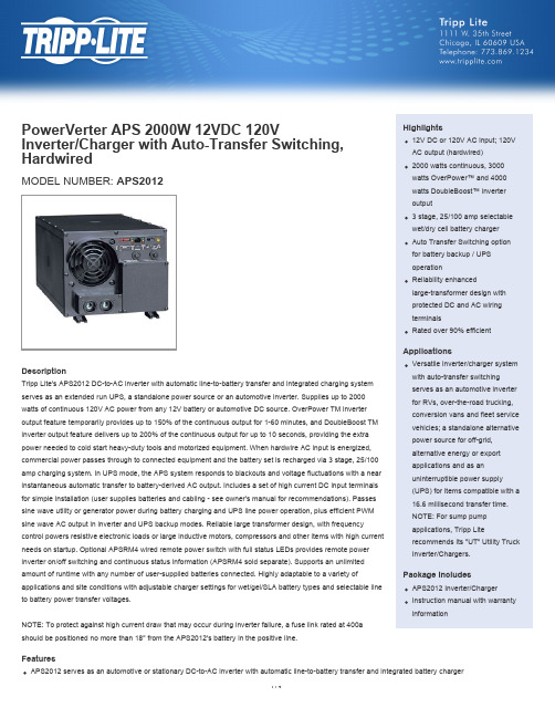
PowerVerter APS 2000W 12VDC 120VInverter/Charger with Auto-Transfer Switching, Hardwired Highlights12V DC or 120V AC input; 120V AC output (hardwired)2000 watts continuous, 3000Supports 120V AC output from a 120V AC line power source or 12V DC battery sourceSupports 120V AC output from a 120V AC 16.6 millisecond automatic transfer between line and battery power supports UPS protection during blackouts and voltage fluctuations for equipment compatible with a one cycle transfer time2000 watts continuous AC output in inverter mode, 2400 watts continuous AC output in AC modeDouble Boost inverter output supports momentary startup loads up to 200% of the continuous rating for up to 10 secondsOverPower inverter output supports longer duration overloads to 150% for 1-60 minutes under ideal battery and temperature conditions. (For best results, utilize OverPower usage for as short of a duration as possible, ensure battery bank and cabling is able to provide full nominal DC voltage under load and allow inverter/charger to fully cool before and after OverPower usage.)3-stage, selectable 25/100 amp battery charger with adjustable settings for wet/gel battery types offers fast, reliable battery rechargingProtected hardwire bolt-down input lugs safely accept heavy gauge input wiring from attached battery bankProtected hardwire output passes 120V line power or inverter output through to connected equipmentReliability enhanced large-transformer design with secure mounting flanges and protected DC wiring terminalsMoisture-resistant construction enables vehicular or marine operation in high humidity environments3 position operating mode switch supports "AUTO" mode to enable automatic transfer between DC and AC modes, CHARGE-ONLY to maintain a fullbattery charge when AC is present without auto transfer and SYSTEM OFF settingsSet of six front panel LEDs display AC/DC operational modes, overload status, DC voltage level, shutdown status and system fault statusSet of 4 configuration dip switches support wet/gel battery charging profiles, adjustable 135/145V high voltage auto transfer during overvoltages and selectable 75/85/95/105V AC low voltage auto transfer during brownoutsSet of 4 additional configuration dip switches support 4 levels of charger limiting relative to output load size, a battery equalization program and battery charger low/high settingsResettable 25A charger AC input breaker and resettable 20A AC output breaker and automatic 2 speed cooling fan protect the inverter from load and temperature related failuresInternal Grounding Terminal properly connects the inverter/charger system to earth ground or vehicle grounding systemAutomatic overload and thermal shutoff safely turns off inverter as excessive loads or overheating conditions developFront panel remote control connector enables remote off/on switching (requires APSRM4 switch accessory). Optional APSRM4 accessory also includes user configurable jacks to support inverter shutoff or startup as a vehicle ignition is engagedLoad sensing control dial enables adjustable load threshold required to automatically turn the inverter on and off in DC mode as load conditions change SpecificationsOVERVIEWStyle Heavy-duty with built-in battery chargerOUTPUTFrequency Compatibility60 HzOutput Receptacles HardwireOutput (Watts)2000Continuous Output Capacity (Watts)2000Peak Output Capacity (Watts)4000Output Nominal Voltage120VOutput Voltage Regulation LINE POWER (AC): Maintains 120V nominal sine wave output from line power source. INVERTER POWER (AC):Maintains PWM sine wave output voltage of 120 V AC (+/-5%).Output Frequency Regulation60 Hz (+/- 0.3 Hz)Overload Protection Includes 25A input breaker dedicated to the charging system and 20A output breaker for AC output loadsINPUTNominal Input Voltage(s) Supported120V ACRecommended Electrical Service DC INPUT: Requires 12V DC input source capable of delivering 192A for the required duration (when used at fullcontinuous capacity - DC requirements increase during Over-Power and Double-Boost operation).Maximum Input Amps / Watts DC INPUT: Full continuous load - 192A at 12V DC. AC INPUT: 38 amps at 120V AC with full inverter and charger load (21A max charger-only / combined input load to support charger and AC output is automatically controllable to 66%-33%-0% based on AC output lInput Connection Type DC INPUT: Set of 2 DC bolt-down terminals. AC INPUT: Hardwire via built in junction box with cover plate. Usersupplies cabling. 4 gauge or larger (see manual). AC INPUT: user supplies hardwire input cabling.Voltage Compatibility (VAC)120Voltage Compatibility (VDC)12BATTERYExpandable Battery Runtime Runtime is expandable with any number of user supplied wet or gel type batteriesDC System Voltage (VDC)12Battery Pack Accessory (Optional)98-121 sealed lead acid battery (optional)Battery Charge25A/100A (selectable)LEDS ALARMS & SWITCHESSwitches 3 position on/off/remote switch enables simple on/off power control plus "auto/remote" setting that enables distant on/off control of the inverter system when used in conjunction with optional APSRM4 accessory when used in inverter mode. In AC uninterruptible power mode, "auto/remote" setting enables automatic transfer from line power to battery power - to maintain continuous AC power to connected loads.Front Panel LEDs Set of 6 LEDs offer continuous status information on load percentage (6 levels reported) and battery charge level (7levels reported). See manual for sequences.SURGE / NOISE SUPPRESSIONAC Suppression Joule Rating600PHYSICALShipping Dimensions (hwd / in.)13.25 x 15 x 21.5Shipping Dimensions (hwd / cm)33.66 x 38.1 x 54.61Shipping Weight (lbs.)43.2Shipping Weight (kg)19.6Unit Dimensions (hwd / in.)7.25 x 8.5 x 16.25Unit Dimensions (hwd / cm)18.42 x 21.59 x 41.28Unit Weight (lbs.)40Unit Weight (kg)18.1Cooling Method Multi-speed fanMaterial of Construction PolycarbonateForm Factors Supported Mounting slots enable permanent placement of inverter on any horizontal surface (see manual for additionalmounting information)ENVIRONMENTALRelative Humidity0-95% non-condensingLINE / BATTERY TRANSFERTransfer Time (Line Power to Battery Mode)16.6 milliseconds (typical - compatible with many computers, servers and networking equipment - verify transfer time compatibility of loads for UPS applications)Low Voltage Transfer to Battery Power In AC "auto" mode, inverter/charger switches to battery mode as line voltage drops to 75V (user adjustable to 85, 95, 105V - see manual)High Voltage Transfer to Battery Power In AC "auto" mode, inverter/charger switches to battery mode as line voltage increases to 135V (user adjustable to 145 - see manual)SPECIAL FEATURESLoad Sensing Optional load sense function enables automatic inverter shutoff and startup as connected equipment is powered off and on. Front panel load sense potentiometer can be set to shutoff or turn on inverter power in response to loads of any level, up to 150 watts.Remote Control Capability YesWARRANTYProduct Warranty Period (U.S. &Canada)1-year limited warrantyProduct Warranty Period(International)2-year limited warrantyProduct Warranty Period (Mexico)2-year limited warrantyProduct Warranty Period (PuertoRico)1-year limited warranty© 2015 Tripp Lite. All rights reserved. All trademarks are the sole property of their respective owners. Tripp Lite has a policy of continuous improvement. Specifications are subject to change without notice. Photos may differ slightly from final products.。
- 1、下载文档前请自行甄别文档内容的完整性,平台不提供额外的编辑、内容补充、找答案等附加服务。
- 2、"仅部分预览"的文档,不可在线预览部分如存在完整性等问题,可反馈申请退款(可完整预览的文档不适用该条件!)。
- 3、如文档侵犯您的权益,请联系客服反馈,我们会尽快为您处理(人工客服工作时间:9:00-18:30)。
由方向相反的两条链路连接。
段(Span):RPR环网上两个相邻节点之间的链路,由方向 相反的两条链路组成。
Copyright © 2009 Huawei Technologies Co., Ltd. All rights reserved.
Page17
RPR环的基本概念(续)
域(Domain):多个连续的段和其上的节点构成域。 节点的东向连接段:指和节点相邻的一个段,该段位于节点 的1环入接口所在的一侧。
Page23
RPR环的保护倒换
当RPR环上节点失效或者链路发生故障的时候,RPR可以通 过自动保护倒换保证环网的连通性,提供相当于SDH APS的 低于50毫秒故障保护能力。RPR的自动保护倒换不需要象
RPR技术综合了SDH/SONET和以太网以及其它一些环网技 术的优点,研究并规范化一种环网拓扑上使用的MAC 层协议 -RPR„弹性分组环‟,满足未来网络的要求。集IP的智能 化、以太网的经济性和光纤环网的高带宽、高可靠性于一体。 提供一种更优的城域网解决方案。 RPR的设计目标定义了一个闭合环路、点到点、基于MAC层
Page14
目 录
环网技术概述 RPR环技术概述 RPR环技术特点
RPR环的基本概念
RPR环的数据操作 RPR环的保护倒换 RPR环的公平算法
Copyright © 2009 Huawei Technologies Co., Ltd. All rights reserved.
Page15
RPR环的基本概念
RPR环的基本概念
RPR环的数据操作 RPR环的保护倒换 RPR环的公平算法
Copyright © 2009 Huawei Technologies Co., Ltd. All rights reserved.
Page12
RPR环技术特点
物理层多样性 带宽高利用率 快速保护机制 公平的节点带宽分配 拓扑自动发现机制,支持即插即用
Page16
RPR环的基本概念(续)
0环(ringlet0):RPR双环中,数据帧发送方向为顺时针的称为0环, 也称“外环”。 1环(ringlet1):RPR双环中,数据帧发送方向为逆时针的称为1环, 也称“内环”。 节点(Station):RPR环网上的设备,它负责接收和转发数据。 链路(Link):连接相邻节点之间的一段传输通道。相邻节点之间
环网技术概述 RPR环技术概述 RPR环技术特点
RPR环的基本概念
RPR环的数据操作 RPR环的保护倒换 RPR环的公平算法
Copyright © 2009 Huawei Technologies Co., Ltd. All rights reserved.
Page19
RPR环的数据操作
在RPR环网中,节点与环配合,采用分组ADM(Add/Drop Multiplexer)式数据交换,完成数据操作。结合下图介绍 RPR环的数据操作:
RPR采用逆向双环结构,数据沿环网在节点之间进行转发。 如图所示是一个典型的RPR环网,以下结合该图介绍几个RPR的基 本概念
节点(Station) 0环(Outer ring)
1环(Inner ring)
链路(Link)
段(Span)
域(Domain)
Copyright © 2009 Huawei Technologies Co., Ltd. All rights reserved.
Copyright © 2009 Huawei Technologies Co., Ltd. All rights reserved.
Page8
环网技术概述(续)
GE/POS,严格来说,并不是一种环网技术,仅仅是近年来, 网络上的一种比较流行的组网应用。将网络上面的N个节点通 过N条链路首尾相连起来,整个环其实是由N个相互独立的点
到点POS/PPP连接构成的,业务在节点间逐点三层转发实现
相互通信,节点需要处理所有报文,严重影响环的吞吐量。 由于仅仅是一个组网性的应用,没有一个针对环级别的带宽 管理,某段的拥塞无法通知其它节点,而且没有二层的故障 自愈能力。
Copyright © 2009 Huawei Technologies Co., Ltd. All rights reserved.
并将数据帧交给节点上层作相应处理。
过环(transit):节点设备将途经本节点的数据流转发到下一 个节点。 剥离(strip):节点设备不再往下转发途经本节点的数据, 即终止数据帧在RPR环网上的转发。
Copyright © 2009 Huawei Technologies Co., Ltd. All rights reserved.
Copyright © 2009 Huawei Technologies Co., Ltd. All rights reserved.
Page7
环网技术概述(续)
SDH/SONET„数字同步系列‟是目前广泛应用在传输网络里面的 一种环网技术,支持单环、多环,具有高可靠性,能提供故障自动 保护倒换APS故障自愈机制。 SDH/SONET采用点到点电路交换的 设计,环内带宽被静态分配为一条条静态固定带宽链路,使用时分 复用,主要为语音服务。由于其点到点电路交换的设计,带来了很 多缺点,如逻辑全连接时带宽浪费严重,带宽在节点间点到点的链 路中固定分配并保留,带宽不能根据网络中流量的实际情况而改变, 不利于带宽的高效利用,很难适应具有突发性特点的IP数据业务。 广播和组播报文将分成多个单播传送,带宽浪费严重,而且对于 APS特性,需要最高多达50%冗余带宽,未能提供灵活的选择机制。
Copyright © 2009 Huawei Technologies Co., Ltd. All rights reserved.
Page22
目 录
环网技术概述 RPR环技术概述 RPR环技术特点
RPR环的基本概念
RPR环的数据操作 RPR环的保护倒换 RPR环的公平算法
Copyright © 2009 Huawei Technologies Co., Ltd. All rights reserved.
修订记录
课程编码
DC232007
本页不打印
适用产品
ALL
产品版本
ALL
课程版本ISSUE
1.00
开发/优化 者
高书颖
时间
2010-3-18
审核人
刘志根
开发类型(新开发/优 化)
新开发
Copyright © 2009 Huawei Technologies Co., Ltd. All rights reserved.
有效支持组播和广播
流量等级保证QoS,支持带宽预留的业务
Copyright © 2009 Huawei Technologies Co., Ltd. All rights reserved.
Page13
Copyright © 2009 Huawei Technologies Co., Ltd. All rights reserved.
Page0
RPR技术
Copyright © 2009 Huawei Technologies Co., Ltd. All rights reserved.
前 言
本课程介绍弹性分组数据环(RPR)技术的基本原理与配置。 RPR技术综合了SDH/SONET和以太网以及其它一些环网技 术的优点,集IP的智能化、以太网的经济性和光纤环网的高
FDDI„光纤分布式数据接口‟可以说是一种改进的Token Ring技术,也是利用令牌来传递对环网的控制权,所不同的 是,他采用了双环结构,采用光纤作为传输介质,在性能和
效率上都较令牌环网有很大提高。但是FDDI和Token Ring一
样,不具备故障自愈的保护功能。由于也是采用源地址剥离 技术,带宽得不到有效利用。FDDI网络目前在企业网和校园 网中得到广泛的应用。
Page9
目 录
环网技术概述 RPR环技术概述 RPR环技术特点
RPR环的基本概念
RPR环的数据操作 RPR环的保护倒换 RPR环的公平算法
Copyright © 2009 Huawei Technologies Co., Ltd. All rights reserved.
Page10
RPR环技术概述
带宽、高可靠性于一体。提供一种更优的城域网解决方案。
Copyright © 2009 Huawei Technologies Co., Ltd. All rights reserved.
Page2
培训目标
学完本课程后,您应该能:
理解RPR技术的基本概念 掌握RPR技术的基本原理
C, Ltd. All rights reserved.
Page5
环网技术概述(续)
Token Ring„令牌环‟是最早引入数据通信领域中的环网技术,是 一个基于MAC层协议的单向环网,用于局域网,不具备故障自愈的 保护功能。令牌环网是一种低速网络,一般在5类线缆上面传送。 令牌环网的节点只有在获得令牌的情况下才能向环上发送数据,令 牌逐点传送,每个节点能轮流拥有一定的令牌时间,节点需要等待 令牌以传送数据。已有令牌的节点,如果没有数据需要传送,可以 将令牌传递给下一个节点。数据包采用源节点剥离的方法,即数据
数据过环
0环数据下环
0环数据上环
1环数据上环
1环(Inner ring)
1环数据下环
Copyright © 2009 Huawei Technologies Co., Ltd. All rights reserved.
Page20
RPR环的数据操作(续)
上环(insert):节点设备把来自环网外的数据帧插入到RPR 环网的数据流中。 下环(copy):节点设备从RPR环网的数据流中接收数据帧,