MM54C904中文资料
数据手册中文版

14位, 165M SPA(采样率)DAC(数模转换器)特性:●单电源供电+5V或+3V●高SFDR (无杂散动态范围): 在100MSPS 64dBc时20MHz输出●低干扰: 3PV -S●低功耗: 170MW (+5 V时)应用●通讯传输通道WLL , 蜂窝基站数字微波链路电缆调制解调器●波形产生直接数字频率合成器(DDS )任意波形发生器(ARB )●医疗/超声●高速仪表和控制●视频, 数字电视说明:DAC904是一款高速数模转换器, 14位分辨率, 引脚兼容DAC908、DAC900、DAC902, 分别提供8-, 10-, 12-位分辨率选择。
该系列DAC支持的所有型号更新率超过165MSPS, 具有优良的动态性能。
DAC904先进分割架构的优化为单音和多频音信号提供高无杂散动态范围(SFDR), 特别是用于通信系统的发送信号电路时。
DAC904具有高阻抗(200KΩ)的电流输出, 标称范围为20mA和一个最多为1.25V的输出。
差分输出允许两个差分或单端模拟信号的接口。
电流输出的匹配保证在差分结构中杰出的动态性能, 它可以与变压器配合使用。
运用一个小的几何CMOS工艺, 单片DAC904可以用在+2.7 V至+5.5 V宽的单电源范围内操作。
其低功耗特性允许它使用在便携式和电池供电系统情况下。
可通过减少输出电流与调整满量程选项实现进一步优化。
DAC904不断运转时, 掉电模式导致其待机功率仅为为45mW 。
DAC904带有一个集成的1.24V带隙基准和边沿触发输入锁存器, 提供完整的转换器解决方案。
+3 V和+5 V CMOS逻辑系列都可以接口到DAC904 。
DAC904的参考结构允许使用芯片上的参考, 或施加外部参考。
通过一个外部电阻, 满量程输出电流可以调整在2 - 20mA, 并保持其指定的动态性能。
DAC904采用SO -28和TSSOP -28封装。
绝对最大额定值+VA到AGND(模拟信号地)......-0.3V至+6V+VD到DGND(数字信号地)......-0.3V到+6VAGND到DGND......-0.3V到+0.3V+VA 到+VD......-6V到+6VCLK, PD到DGND......-0.3V到VD+0.3VD0-D13到DGND......-0.3V到VD+0.3VIOUT, I 到AGND......-1V到VA+0.3VBW,BYP到AGND......-0.3V到VA+0.3VREFIN ,FSA到AGND......-0.3V到VA+0.3VINT/EXT到AGND......-0.3V到VA+0.3V结温度. . . . . . . +150℃存储器温度. . . . . . +125℃防静电敏感度这种集成的电路可以被ESD(静电释放)损坏。
MM54HC191中文资料

TL F 5322MM54HC190 MM74HC190 MM54HC191 MM74HC191January1988 MM54HC190 MM74HC190SynchronousDecade Up Down Counters with ModeControl MM54HC191 MM74HC191Synchronous Binary Up Down Counterswith Mode ControlGeneral DescriptionThese high speed synchronous counters utilize advancedsilicon-gate CMOS technology They possess the high noiseimmunity and low power consumption of CMOS technologyalong with the speeds of low power Schottky TTLThese circuits are synchronous reversible up down count-ers The MM54HC191 MM74HC191are4-bit binary count-ers and the MM54HC190 MM74HC190are BCD countersSynchronous operation is provided by having all flip-flopsclocked simultaneously so that the outputs change simulta-neously when so instructed by the steering logic This modeof operation eliminates the output counting spikes normallyassociated with asynchronous(ripple clock)countersThe outputs of the four master-slave flip-flops are triggeredon a low-to-high level transition of the clock input if theenable input is low A high at the enable input inhibits count-ing The direction of the count is determined by the level ofthe down up input When low the counter counts up andwhen high it counts downThese counters are fully programmable that is the outputsmay be preset to either level by placing a low on the loadinput and entering the desired data at the data inputs Theoutput will change independent of the level of the clock in-put This feature allows the counters to be used as modulo-N dividers by simply modifying the count length with thepreset inputsTwo outputs have been made available to perform the cas-cading function ripple clock and maximum minimum countThe latter output produces a high-level output pulse with aduration approximately equal to one complete cycle of theclock when the counter overflows or underflows The rippleclock output produces a low-level output pulse equal inwidth to the low-level portion of the clock input when anoverflow or underflow condition exists The counters can beeasily cascaded by feeding the ripple clock output to theenable input of the succeeding counter if parallel clocking isused or to the clock input if parallel enabling is used Themaximum minimum count output can be used to accom-plish look-ahead for high-speed operationFeaturesY Level changes on Enable or Down Up can be made re-gardless of the level of the clock inputY Wide power supply range 2–6VY Low quiescent supply current 80m A maximum(74HC Series)Y Low input current 1m A maximumConnection DiagramDual-In-Line PackageTL F 5322–1Top ViewLoadEnable DownClock FunctionG UpH L L u Count UpH L H u Count DownL X X X LoadH H X X No ChangeAsynchronous inputs Low input to load sets Q A e AQ B e B Q C e C and Q D e DOrder Number MM54HC190 191or MM74HC190 191C1995National Semiconductor Corporation RRD-B30M105 Printed in U S AAbsolute Maximum Ratings(Notes1 2) If Military Aerospace specified devices are required please contact the National Semiconductor Sales Office Distributors for availability and specifications Supply Voltage(V CC)b0 5to a7 0V DC Input Voltage(V IN)b1 5to V CC a1 5V DC Output Voltage(V OUT)b0 5to V CC a0 5V Clamp Diode Current(I IK I OK)g20mA DC Output Current per pin(I OUT)g25mA DC V CC or GND Current per pin(I CC)g50mA Storage Temperature Range(T STG)b65 C to a150 C Power Dissipation(P D)(Note3)600mW S O Package only500mW Lead Temp (T L)(Soldering10seconds)260 C Operating ConditionsMin Max Units Supply Voltage(V CC)26V DC Input or Output Voltage0V CC V (V IN V OUT)Operating Temp Range(T A)MM74HC b40a85 C MM54HC b55a125 C Input Rise or Fall TimesV CC e2 0V(t r t f)1000ns V CC e4 5V500nsV CC e6 0V400nsDC Electrical Characteristics(Note4)T A e25 C 74HC54HCSymbol Parameter Conditions V CC T A eb40to85 C T A eb55to125 C UnitsTyp Guaranteed LimitsV IH Minimum High Level V V Input Voltage V VV VV IL Maximum Low Level V V Input Voltage V VV VV OH Minimum High Level V IN e V IH or V ILOutput Voltage l I OUT l s m A V VV VV VV IN e V IH or V ILl I OUT l s mA V Vl I OUT l s mA V V V OL Maximum Low Level V IN e V IH or V ILOutput Voltage l I OUT l s m A V VV VV VV IN e V IH or V ILl I OUT l s mA V Vl I OUT l s mA V V I IN Maximum Input V IN e V CC or GND V g g g m ACurrentI CC Maximum Quiescent V IN e V CC or GND V m ASupply Current I OUT e m ANote1 Absolute Maximum Ratings are those values beyond which damage to the device may occurNote2 Unless otherwise specified all voltages are referenced to groundNote3 Power Dissipation temperature derating plastic‘‘N’’package b12mW C from65 C to85 C ceramic‘‘J’’package b12mW C from100 C to125 C Note4 For a power supply of5V g10%the worst case output voltages(V OH and V OL)occur for HC at4 5V Thus the4 5V values should be used when designing with this supply Worst case V IH and V IL occur at V CC e5 5V and4 5V respectively (The V IH value at5 5V is3 85V )The worst case leakage current(I IN I CC and I OZ)occur for CMOS at the higher voltage and so the6 0V values should be usedV IL limits are currently tested at20%of V CC The above V IL specification(30%of V CC)will be implemented no later than Q1 CY’892AC Electrical Characteristics T A e25 C V CC e5 0V t r e t f e6ns C L e15pF(unless otherwise specified)Symbol ParameterFrom ToTyp Units (Input)(Output)f MAX Maximum Clock MHzFrequencyt PLH t PHL Maximum Propagation Delay Time Load Q A Q B nsQ C Q Dt PLH t PHL Maximum Propagation Delay Time Data A Q A Q B nsB C D Q C Q Dt PLH t PHL Maximum Propagation Delay Time Clock Ripple nsClockt PLH t PHL Maximum Propagation Delay Time Clock Q A Q B nsQ C Q Dt PLH t PHL Maximum Propagation Delay Time Clock Max Min nst PLH t PHL Maximum Propagation Delay Time Down Up Ripple nsClockt PLH t PHL Maximum Propagation Delay Time Down Up Max Min ns t PHL t PLH Maximum Propagation Delay Time Enable Ripple Clock nst W Minimum Clock Clear or Load ns Input Pulse WidthAC Electrical Characteristics V CC e2 0V to6 0V C L e50pF t r e t f e6ns(unless otherwise specified)From To T A e25 C 74HC54HCSymbol Parameter(Input)(Output)V CC T A e b40to85 C T A eb55to125 C UnitsTyp Guaranteed Limitsf MAX Maximum Clock V MHzFrequency V MHzV MHz t PLH t PHL Maximum Propagation Load Q A Q B V ns Delay Time Q C Q D V nsV ns t PLH t PHL Maximum Propagation Data A Q A Q B V ns Delay Time B C D Q C Q D V nsV ns t PLH t PHL Maximum Propagation Clock Ripple V ns Delay Time Clock V nsV ns t PLH t PHL Maximum Propagation Clock Q A Q B V ns Delay Time Q C Q D V nsV ns3AC Electrical Characteristics(Continued)Symbol ParameterFrom ToConditions V CCT A e25 C74HC54HCUnits (Input)(Output)T A eb40to85 C T A eb55to125 CTyp Guaranteed Limitst PLH t PHL Maximum Propagation Clock Max Min V ns Delay Time V nsV nst PLH t PHL Maximum Propagation Down Up Ripple V ns Delay Time Clock V nsV nst PLH t PHL Maximum Propagation Down Up Max Min V ns Delay Time V nsV nst PHL t PLH Maximum Propagation Enable Ripple V ns Delay Time Clock V nsV nst W Minimum Clock Load or V ns Clear Input Pulse Width V nsV nst S Minimum Setup Time Data Load V nsV nsV nst H Data Hold Time Load Data V b nsV b nsV b nst S Minimum Setup Time Down Up Clock V nsV nsV nst H Minimum Hold Time Clock Down Up V b nsV b nsV b nst S Minimum Setup Time Enable Clock V nsV nsV nst H Minimum Hold Time Clock Enable V b nsV b nsV b nst rem Minimum Removal Time Load Clock V nsV nsV nst THL t TLH Maximum Output V s Rise and Fall Time V nsV nst W Minimum Load V ns Pulse Width V nsV nsC IN Input Capacitance pFC PD Power Dissipation pFCapacitance NoteNote5 C PD determines the no load dynamic power consumption P D e C PD V CC2f a I CC V CC and the no load dynamic current consumption I S e C PD V CC f aI CC4Logic Diagrams’HC190Decade CountersTL F 5322–2 Pin(16)e V CC Pin(8)e GND5Logic Diagrams(Continued)’HC191Binary CountersTL F 5322–3Pin(16)e V CC Pin(8)e GND6Timing Diagrams’HC190Synchronous Decade CountersTypical Load Count and Inhibit SequencesTL F 5322–4Sequence(1)Load(preset)to BCD seven(2)Count up to eight nine zero one and two(3)Inhibit(4)Count down to one zero nine eight and seven’HC191Synchronous Binary CountersTypical Load Count and Inhibit SequenceTL F 5322–5Sequence(1)Load(preset)to binary thirteen(2)Count up to fourteen fifteen zero one and two(3)Inhibit(4)Count down to one zero fifteen fourteen and thirteen7M M 54H C 190 M M 74H C 190 M M 54H C 191 M M 74H C 191Physical Dimensions inches (millimeters)Order Number MM54HC190J MM54HC191J MM74HC190J or MM74HC191JNS Package J16AOrder Number MM74HC190N or MM74HC191NNS Package N16ELIFE SUPPORT POLICYNATIONAL’S PRODUCTS ARE NOT AUTHORIZED FOR USE AS CRITICAL COMPONENTS IN LIFE SUPPORT DEVICES OR SYSTEMS WITHOUT THE EXPRESS WRITTEN APPROVAL OF THE PRESIDENT OF NATIONAL SEMICONDUCTOR CORPORATION As used herein 1 Life support devices or systems are devices or 2 A critical component is any component of a life systems which (a)are intended for surgical implant support device or system whose failure to perform can into the body or (b)support or sustain life and whose be reasonably expected to cause the failure of the life failure to perform when properly used in accordance support device or system or to affect its safety or with instructions for use provided in the labeling can effectivenessbe reasonably expected to result in a significant injury to the userNational Semiconductor National Semiconductor National Semiconductor National Semiconductor CorporationEuropeHong Kong LtdJapan Ltd1111West Bardin RoadFax (a 49)0-180-530858613th Floor Straight Block Tel 81-043-299-2309。
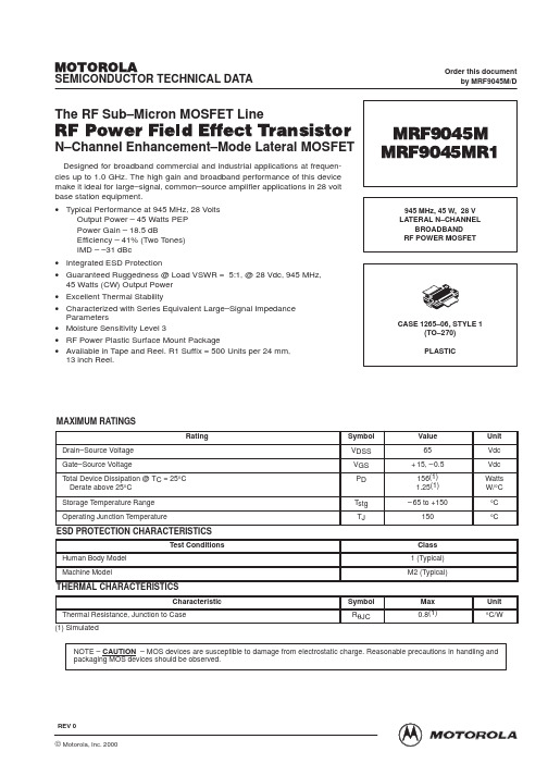
MRF9045M中文资料
Z3 Z4 Z5 Z6 Z7 Z8 Z9 Z10 Z11 Z12 Z13
0.14″ x 0.32″ 0.47″ x 0.32″ 0.16″ x 0.32″ x 0.62″ Tapered 0.18″ x 0.62″ 0.56″ x 0.62″ 0.33″ x 0.32″ 0.14″ x 0.32″ 0.36″ x 0.08″ 1.01″ x 0.08″ 0.15″ x 0.08″ 0.29″ x 0.08″
N–Channel Enhancement–Mode Lateral MOSFET
MRF9045M MRF9045MR1
945 MHz, 45 W, 28 V LATERAL N–CHANNEL BROADBAND RF POWER MOSFET
CASE 1265–06, STYLE 1 (TO–270) PLASTIC
mrf9045m中文资料lm358中文资料12864中文资料lm393中文资料mpu6050中文资料lm324中文资料7805中文资料max232中文资料tl431中文资料op07中文资料74hc595中文资料
元器件交易网
MOTOROLA
SEMICONDUCTOR TECHNICAL DATA
MAXIMUM RATINGS
Rating Drain–Source Voltage Gate–Source Voltage Total Device Dissipation @ TC = 25°C Derate above 25°C Storage Temperature Range Operating Junction Temperature Symbol VDSS VGS PD Tstg TJ Value 65 + 15, – 0.5 156(1) 1.25(1) – 65 to +150 150 Unit Vdc Vdc Watts W/°C °C °C
AR904进程分析仪说明书

USER MANUALPROCESS ANALOGUE CALIBRATORAR904Version 1.1.12013.02.13Thank you for choosing our product.This user manual will help you with proper and safeoperation and full use of the process analogue calibrator device.Before installing and operating, please readand understand this manual.If you have any additional questions, please contact the technical advisor. TABLE OF CONTENTSPay special attention to information marked with this sign!Manufacturer reserves the right to make changes in design and software of the device without compromising technical parameters1.SAFETY PRECAUTIONS▪Before using the unit, please read this manual carefully.▪To avoid electrical shock or damage to the device, mechanical and electrical installation have to be performed by a qualified personnel.▪Before turning on the power make sure that all cables are properly connected.▪Before making any modifications to the wiring connections, turn off all voltages applied to the device. ▪You have to ensure proper working conditions, according to the specifications of the device (power supply voltage, humidity, temperature, chapter 5).2.INSTALLATION NOTESThis instrument was designed to provide the appropriate level of resistance to most disturbances that may occur in industrial environments. In environments with unknown level of interference it is recommended to use the following measures to prevent possible interference with operation of the instrument:▪Do not power supply the device from the same line as the power component without the appropriate network filters.▪Use only shielded power and signal cables taking into account that the grounding of the shield should bea single point, made as close to the device as possible.▪Avoid placing signal cables very close and parallel to energy and power cables.▪It is recommended to twist signal cables in pairs.▪Avoid proximity of remote controlled devices, electromagnetic meters, high power loads, loads with phase or group power control and other devices that generate large impulse disturbances.▪Ground or zero metal rails that are used to mount rail devices.Before using the device, remove the protective film from the LED display.3.GENERAL PROCESS ANALOGUE CALIBRATOR CHARACTERISTICS▪This device allows you to control or test devices with current or voltage input (proportional valves, servomotors, inverters, motors, etc.)▪ 2 analogue outputs (working simultaneously):-current 4÷20mA or 0÷20mA (active, cannot be powered from 2 wires current loop)-voltage 0÷10V▪Soft start/stop (ramping) or triangle wave generator with manual or automatic (activated after device power on) trigger.▪Programmable setpoint value, output signal change step, display range, soft start/stop options, communication options, access options and other configuration parameters.▪7-segment LED display with brightness adjustment.▪Optional RS485/RS232 serial interface (galvanically isolated, MODBUS-RTU protocol).▪Parameters configuration methods:-Using IP65 foil keyboard located on the device front panel-Using AR955 programmer or RS485/RS232 interface with PC software (Windows 2000/XP/Vista/7)▪Available free software that allows parameters configuration.▪Access to configuration parameters can be password protected.▪High accuracy and high resistance to interference.▪Available accessories:-AR955 programmer-RS485 to USB converterCAUTION:Before starting work with the process analogue calibrator, read this manual carefully and perform electrical and mechanical installation properly and set parameters correctly.4.PACKAGE CONTENTS▪Process analogue calibrator▪User manual▪Warranty card5.TECHNICAL DATA(1)- Output cannot be powered from two wires current loop6.HOUSING DIMMENSIONS AND INSTALLATION DATA7.TERMINAL STRIPS AND ELECTRICAL CONNECTIONS DESCRIPTIONa)Terminals and output signals descriptionOnly AR955 programmer can be connected to PRG socket. Connecting other devices to PRG socket can damage connected device and AR904 process analogue calibrator.8.BUTTONS DESCRIPTIONa) Buttons functions in setpoint value display mode (normal mode)) )and 9: b) Buttons functions in parameters configuration mode (chapter 10)9.OUTPUTS SETPOINT VALUE CHANGEPressing [UP] or [DOWN] button while setpoint value is being displayed will change the value by pre-set step(parameter 6: , chapter 10, table 10). Changes of the output signal are proportional to changes of the displayed value. Pressing [SET] + [DOWN] buttons together will set output value immediately to lower rangevalue (2: or 4: ) while pressing [SET] + [UP] buttons together will set output value immediately to upperrange value (3: or 5: ). In addition, the output signal may be given also in parameters programming mode(parameter 7: ) and using serial interface RS485/RS232 or AR955 programmer (chapter 15, table 15). Moreover, it is possible to set the setpoint value outside of the display range based on the parameters 2: and 3:. The value of this override that can be set using the buttons is ±5% for 4÷20mA (2÷10V) output and 6,2% for the remaining outputs.10.CONFIGURATION PARAMETERS SETUPAll configuration parameters of the device are saved in the non-volatile EEPROM internal memory. Two parameters configuration methods are available:ing IP65 foil keyboard located on the front panel of the device:-From the setpoint value display mode enter configuration menu (press and hold for more than 1 second [UP] and [DOWN] buttons together). If parameter 13: (password protection is turned on), display will show message and then with first digit blinking. Using [UP] or [DOWN] button enter protection password (by default parameter 12: ). To proceed to the next digit or confirm the code use [SET] button.-After opening configuration menu you will see mnemonic parameter names ( <-> <-> <-> etc.), [UP] button will proceed to the next parameter and [DOWN] button will go back to theprevious parameter (all parameters are listed in table 10).-To change or display current parameter value press the [SET] button.-Using [UP] or [DOWN] button change the edited parameter value.-Confirm modified value using [SET] button or cancel using [UP] and [DOWN] buttons (simultaneously), then parameter name will be displayed.ing RS485/RS232 port or AR955 programmer and pc software ARSOFT-WZ1:-Connect process analogue calibrator to the PC port and start ARSOFT-WZ1 application.-After connection is established application window will display current setpoint value.-Device parameters can be displayed and modified in the parameters configuration window.-New paramete rs values have to be saved using “Zatwierdź zmiany” button.-Current configuration can be saved in a file or can be read from the file.CAUTION:-Do not use RS485/RS232 port and AR955 programmer simultaneously, because communication errors will occur.Table 10. Configuration parameters0: currentdot position(0.0)display units – display for 0mA, 4mA, 0V – lower output rangedisplay units – display for 20mA, 10V – upper output rangesetpoint units – lower setpoint value limit (parameter 7: )when set using buttonssetpoint units – upper setpoint value limit (parameter 7: )when set using buttonsvalue units, setpoint value change step (parameter 7: ) when setusing buttonssetpoint or 4:or 5: , changes step: 6:soft start The duration of the rising edge (ramp). Function isturned on for value (description in chapter 11) soft stop The duration of the falling edge (ramp). Function isturned on for value (description in chapter 11) rampsetpointdisplay (10% step)RS485/RS232 kbit/s kbit/s kbit/s kbit/s kbit/s kbit/s11.SOFT START/STOP AND TRIANGLE WAVEFORM GENERATORThis device has soft start and stop (ramp) function. This function works as shown on the below charts (illustrations 11.1, 11.2, 11,3). To turn on this function you will have to configure soft start time (rising slope,parameter 8: , chapter 10) or soft stop time (falling slope, parameter 9: ) and trigger mode (parameter10: ). If both times are different than 0 (8: and 9: ) device outputs will generate triangle periodicalsignal. Amplitudes (end values) of output signals are defined by parameter 2: , 3: , 4: and 5:. Function is activated automatically after device power on (when parameter 10: ) or manually (10: ) using [SET] button (pressed and hold for more than 1.5 seconds). Moreover ramp function can be stopped and resumed at any time using [SET] button (short message will be displayed - start or - stop). Output status in this mode is refreshed 4 times per second.Illustration 11.1. Output status in soft start mode (parameter ).Illustration 11.2. Output status in soft stop mode (parameter ).Illustration 11.3. Output status in triangle signal generator mode (parameter ).12.MESSAGES AND ERRORS LISTFollowing short messages can be displayed during device operation:13.RS485 COMMUNICATION INTERFACE (per EIA RS-485)Maximum RS485 cable length – 1km.Maximum number of devices in RS485 line – 30. To increase this number you can use RS485/RS485 repeater. Terminal resistors when MASTER is on the line beginning (above illustration):-On the line beginning –2 x 820Ω to ground and +5V of the MASTER and 150Ω between lines,- On the line end - 150Ω between lines.Terminal resistors when MASTER is in the middle of the line:- Near the converter – 2 x 820Ω to ground and +5V of the converter, - On both line ends – each end 150Ω between lines.14. RS232C COMMUNICATION INTERFACE (per EIA RS-232C)15. MODBUS-RTU SERIAL TRANSMISSION PROTOCOL Character format:8 bits, 1 stop bit, no parity bitAvailable functions: READ – 3 or 4, WRITE – 6Table 15.1. Request frame format for READ function (frame length – 8 Bytes):Table 15.2. Request frame format for WRITE function (frame length– 8 Bytes):Table 15.3. Response frame format for READ function (minimum frame length – 7 Bytes):Table 15.4. Response frame format for WRITE function (frame length – 8 Bytes):Table 15.5. Special response (errors: function field = 0x84 or 0x83 for READ function and 0x86 for WRITE function):Table 15.6. MODBUS-RTU protocol registers mapParameter 0:Parameter 1: dot positionParameter 2: display lower rangeParameter 3:Parameter 4:Parameter 5:Parameter 6:Parameter 7:Parameter 8:Parameter 9:Parameter 10:Parameter 11:Parameter 12:Parameter 13:Parameter 14:Parameter 15:Parameter 16:ER NOTES。
DAC904E中文资料

DESCRIPTION
The DAC904 is a high-speed, Digital-to-Analog Converter (DAC) offering a 14-bit resolution option within the family of highperformance converters. Featuring pin compatibility among family members, the DAC908, DAC900, and DAC902 provide a component selection option to an 8-, 10-, and 12-bit resolution, respectively. All models within this family of DACs support update rates in excess of 165MSPS with excellent dynamic performance, and are especially suited to fulfill the demands of a variety of applications.
The advanced segmentation architecture of the DAC904 is optimized to provide a high Spurious-Free Dynamic Range (SFDR) for single-tone, as well as for multi-tone signals— essential when used for the transmit signal path of communication systems.
The DAC904 is available in SO-28 and TSSOP-28 packages.
REF54_中文样本

标准功能用于逻辑编程,例如电气操作联锁、 继电器同时具有9 个传感器输入。电流传感
5
设计(续)
6
REF541 / 543 / 545 馈 线 终 端
1MRS 755420
器( R o g o w s k i 线圈)或电压传感器可以被 连接到任意传感器输入口上。接线图详见 有 关 图 纸 。需 要 订 货 时 ,请 注 明 模 拟 量 输 入 的类型。
电流保护既可以用Rogowski 线圈也可以用常 CAP501 和 CAP505 整定软件支持 DR-Col-
规的 CT。同样,电压保护可以用电压传感器也 lector工具。
可以用常规的 PT。
电能质量监测功能
关于功能分级和保护功能的详细资料可以参考 电能质量监测功能可以测量电压和电流的总谐
“订货”章节中的表“功能分级,保护功能”。 波畸变率 (THD)以及电流的总需量谐波畸变
10 个(使用传感器)模拟量通道。所使用的通
通讯功能
道数量取决于继电器的配置和所使用的互感器
R E F 5 4 _ 馈线终端支持五种通讯规约: 或传感器的匹配类型。
IEC_103,SPA,LON,DNP 3.0 和 Modbus。
除了常规的 CT 和 PT 外,ABB 公司开发的
标准功能
传感器能同时用在 REF54_ 馈线终端上,
通道之间也是隔离的。模拟量输出可以用作测 量或计算信息传到盘表或 P L C 等。
三个 ● 用于设备控制的按钮(合,分,对象选 择)
LED 指示灯 馈线终端具有 8 个 LED 指示灯,用继电器配置 工具软件可以对 LED 进行参数化。可以任意设 定 LED 的颜色(绿、黄、红)、所关联的信号 和常亮/常暗状态,并具有三种信号驱动模式: 信号不保持、信号保持常亮和信号保持闪烁。 报警信号可由远方、就地或者通过使用馈线终 端的逻辑来复归。
MM74C923中文资料

TL F 6037MM54C922 MM74C92216-Key Encoder MM54C923 MM74C92320-Key EncoderJuly 1993MM54C922 MM74C92216-Key Encoder MM54C923 MM74C92320-Key EncoderGeneral DescriptionThese CMOS key encoders provide all the necessary logic to fully encode an array of SPST switches The keyboard scan can be implemented by either an external clock or external capacitor These encoders also have on-chip pull-up devices which permit switches with up to 50k X on resist-ance to be used No diodes in the switch array are needed to eliminate ghost switches The internal debounce circuit needs only a single external capacitor and can be defeated by omitting the capacitor A Data Available output goes to a high level when a valid keyboard entry has been made The Data Available output returns to a low level when the en-tered key is released even if another key is depressed The Data Available will return high to indicate acceptance of the new key after a normal debounce period this two-key roll-over is provided between any two switchesAn internal register remembers the last key pressed even after the key is released The TRI-STATE outputs provide for easy expansion and bus operation and are LPTTL com-patibleFeaturesY 50k X maximum switch on resistance Y On or off chip clockY On-chip row pull-up devices Y 2key roll-overY Keybounce elimination with single capacitor Y Last key register at outputsY TRI-STATE outpust LPTTL compatible Y Wide supply range3V to 15VYLow power consumptionConnection DiagramsPin Assignment for Dual-In-Line PackageTL F 6037–1Top ViewOrder Number MM54C922orMM74C922Pin Assignmentfor SOICTL F 6037–14Top ViewOrder Number MM74C922Pin Assignment for DIP and SOIC PackageTL F 6037–2Top ViewOrder Number MM54C923orMM74C923TRI-STATE is a registered trademark of National Semiconductor Corporation C 1995National Semiconductor CorporationRRD-B30M105 Printed in U S AAbsolute Maximum Ratings(Note1)If Military Aerospace specified devices are required please contact the National Semiconductor Sales Office Distributors for availability and specifications Voltage at Any Pin V CC b0 3V to V CC a0 3V Operating Temperature RangeMM54C922 MM54C923b55 C to a125 C MM74C922 MM74C923b40 C to a85 C Storage Temperature Range b65 C to a150 C Power Dissipation(P D)Dual-In-Line700mW Small Outline500mW Operating V CC Range3V to15V V CC18V Lead Temperature(Soldering 10seconds)260 CDC Electrical Characteristics Min Max limits apply across temperature range unless otherwise specified Symbol Parameter Conditions Min Typ Max UnitsCMOS TO CMOSV T a Positive-Going Threshold Voltage V CC e5V I IN t0 7mA3 03 64 3V at Osc and KBM Inputs V CC e10V I IN t1 4mA6 06 88 6VV CC e15V I IN t2 1mA9 01012 9V V T b Negative-Going Threshold Voltage V CC e5V I IN t0 7mA0 71 42 0V at Osc and KBM Inputs V CC e10V I IN t1 4mA1 43 24 0VV CC e15V I IN t2 1mA2 156 0V V IN(1)Logical‘‘1’’Input Voltage V CC e5V3 54 5V Except Osc and KBM Inputs V CC e10V8 09VV CC e15V12 513 5V V IN(0)Logical‘‘0’’Input Voltage V CC e5V0 51 5V Except Osc and KBM Inputs V CC e10V12VV CC e15V1 52 5V I rp Row Pull-Up Current at Y1 Y2 V CC e5V V IN e0 1V CC b2b5m AY3 Y4and Y5Inputs V CC e10V b10b20m AV CC e15V b22b45m A V OUT(1)Logical‘‘1’’Output Voltage V CC e5V I O e b10m A4 5VV CC e10V I O e b10m A9VV CC e15V I O e b10m A13 5V V OUT(0)Logical‘‘0’’Output Voltage V CC e5V I O e10m A0 5VV CC e10V I O e10m A1VV CC e15V I O e10m A1 5V R on Column‘‘ON’’Resistance at V CC e5V V O e0 5V5001400X X1 X2 X3and X4Outputs V CC e10V V O e1V300700XV CC e15V V O e1 5V200500X I CC Supply Current V CC e5V0 551 1mAOsc at0V (one Y low)V CC e10V1 11 9mAV CC e15V1 72 6mAI IN(1)Logical‘‘1’’Input Current V CC e15V V IN e15V0 0051 0m Aat Output EnableI IN(0)Logical‘‘0’’Input Current V CC e15V V IN e0V b1 0b0 005m Aat Output EnableCMOS LPTTL INTERFACEV IN(1)Logical‘‘1’’Input Voltage 54C V CC e4 5V V CC b1 5V Except Osc and KBM Inputs74C V CC e4 75V V CC b1 5V V IN(0)Logical‘‘0’’Input Voltage 54C V CC e4 5V0 8V Except Osc and KBM Inputs74C V CC e4 75V0 8VV OUT(1)Logical‘‘1’’Output Voltage54C V CC e4 5V2 4VI O e b360m A74C V CC e4 75V2 4VI O e b360m AV OUT(0)Logical‘‘0’’Output Voltage54C V CC e4 5V0 4VI O e b360m A74C V CC e4 75V0 4VI O e b360m ANote1 ‘‘Absolute Maximum Ratings’’are those values beyond which the safety of the device cannot be guaranteed Except for‘‘Operating Temperature Range’’they are not meant to imply that the devices should be operated at these limits The table of‘‘Electrical Characteristics’’provides conditions for actual device operation2DC Electrical CharacteristicsMin Max limits apply across temperature range unless otherwise specified (Continued)Symbol Parameter ConditionsMinTypMaxUnitsOUTPUT DRIVE (See 54C 74C Family Characteristics Data Sheet)(Short Circuit Current)I SOURCE Output Source Current V CC e 5V V OUT e 0V b 1 75b 3 3mA (P-Channel)T A e 25 CI SOURCE Output Source Current V CC e 10V V OUT e 0V b 8b 15mA (P-Channel)T A e 25 CI SINK Output Sink Current V CC e 5V V OUT e V CC 1 753 6mA (N-Channel)T A e 25 CI SINKOutput Sink Current V CC e 10V V OUT e V CC 816mA(N-Channel)T A e 25 CAC Electrical Characteristics T A e 25 C C L e 50pF unless otherwise notedSymbol ParameterConditionsMinTyp Max Units t pd0 t pd1Propagation Delay Time to C L e 50pF (Figure 1)Logical ‘‘0’’or Logical ‘‘1’’V CC e 5V 60150ns from D AV CC e 10V 3580ns V CC e 15V2560ns t 0H t 1HPropagation Delay Time from R L e 10k C L e 10pF (Figure 2)Logical ‘‘0’’or Logical ‘‘1’’V CC e 5V R L e 10k 80200ns into High Impedance State V CC e 10V C L e 10pF 65150ns V CC e 15V50110ns t H0 t H1Propagation Delay Time from R L e 10k C L e 50pF (Figure 2)High Impedance State to a V CC e 5V R L e 10k 100250ns Logical ‘‘0’’or Logical ‘‘1’’V CC e 10V C L e 50pF 55125ns V CC e 15V 4090ns C IN Input CapacitanceAny Input (Note 2)57 5pF C OUTTRI-STATE Output CapacitanceAny Output (Note 2)10pFAC Parameters are guaranteed by DC correlated testingNote 1 ‘‘Absolute Maximum Ratings’’are those values beyond which the safety of the device cannot be guaranteed Except for ‘‘Operating Temperature Range’’they are not meant to imply that the devices should be operated at these limits The table of ‘‘Electrical Characteristics’’provides conditions for actual device operationNote 2 Capacitance is guaranteed by periodic testingSwitching Time WaveformsTL F 6037–3T1 T2 RC T3 0 7RC where R 10k and C is external capacitor at KBM inputFIGURE 1TL F 6037–4FIGURE 23Block DiagramTL F 6037–5 Truth TableSwitch012345678910111213141516171819 Position Y1 X1Y1 X2Y1 X3Y1 X4Y2 X1Y2 X2Y2 X3Y2 X4Y3 X1Y3 X2Y3 X3Y3 X4Y4 X1Y4 X2Y4 X3Y4 X4Y5 X1Y5 X2Y5 X3Y5 X4 DA A01010101010101010101 T B00110011001100110011 A C00001111000011110000 O D00000000111111110000 U E 00000000000000001111 TOmit for MM54C922 MM74C9224Typical Performance CharacteristicsTypical I rp vs V IN at Any Y InputTL F 6037–6Typical R on vs V OUT at Any X OutputTL F 6037–7Typical F SCAN vs C OSCTL F 6037–8Typical Debounce Period vs C KBMTL F 6037–9Typical ApplicationsSynchronous Handshake (MM74C922)TL F 6037–10Synchronous Data Entry Onto Bus (MM74C922)TL F 6037–11Outputs are enabled when valid entry is made and go into TRI-STATE when key is releasedNote 3 The keyboard may be synchronously scanned by omitting the capacitor at osc and driving osc directly if the system clock rate is lower than 10kHz5Typical Applications(Continued)Asynchronous Data Entry Onto Bus(MM74C922)TL F 6037–12Outputs are in TRI-STATE until key is pressed then data is placed on busWhen key is released outputs return to TRI-STATEExpansion to32Key Encoder(MM74C922)TL F 6037–13 Theory of OperationThe MM74C922 MM74C923Keyboard Encoders imple-ment all the logic necessary to interface a16or20SPST key switch matrix to a digital system The encoder will con-vert a key switch closer to a4(MM74C922)or 5(MM74C923)bit nibble The designer can control both the keyboard scan rate and the key debounce period by altering the oscillator capacitor C OSE and the key bounce mask capacitor C MSK Thus the MM74C922 MM74C923’s per-formance can be optimized for many keyboardsThe keyboard encoders connect to a switch matrix that is4 rows by4columns(MM74C922)or5rows by4columns (MM74C923) When no keys are depressed the row inputs are pulled high by internal pull-ups and the column outputs sequentially output a logic‘‘0’’ These outputs are open drain and are therefore low for25%of the time and other-wise off The column scan rate is controlled by the oscillator input which consists of a Schmitt trigger oscillator a2-bit counter and a2–4-bit decoderWhen a key is depressed key0 for example nothing will happen when the X1input is off since Y1will remain high When the X1column is scanned X1goes low and Y1will go low This disables the counter and keeps X1low Y1goinglow also initiates the key bounce circuit timing and locks out the other Y inputs The key code to be output is a combina-tion of the frozen counter value and the decoded Y inputs Once the key bounce circuit times out the data is latched and the Data Available(DAV)output goes highIf during the key closure the switch bounces Y1input will go high again restarting the scan and resetting the key bounce circuitry The key may bounce several times but as soon as the switch stays low for a debounce period the closure is assumed valid and the data is latchedA key may also bounce when it is released To ensure thatthe encoder does not recognize this bounce as another key closure the debounce circuit must time out before another closure is recognizedThe two-key roll-over feature can be illustrated by assuminga key is depressed and then a second key is depressedSince all scanning has stopped and all other Y inputs are disabled the second key is not recognized until the first key is lifted and the key bounce circuitry has resetThe output latches feed TRI-STATE which is enabled when the Output Enable(OE)input is taken low6Physical Dimensions inches(millimeters)Ceramic Dual-In-Line Package(J)Order Number MM54C922J or MM74C922JNS Package Number J18ACeramic Dual-In-Line Package(J)Order Number MM54C923J or MM74C923JNS Package Number J20A7Physical Dimensions inches(millimeters)(Continued)Plastic Small Outline I C Package(M)Order Number MM74C922M or MM74C923MNS Package Number M20B8Physical Dimensions inches(millimeters)(Continued)Plastic Dual-In-Line Package(N)Order Number MM54C922N or MM74C922NNS Package Number N18A9M M 54C 922 M M 74C 92216-K e y E n c o d e r M M 54C 923 M M 74C 92320-K e y E n c o d e rPhysical Dimensions inches (millimeters)(Continued)Plastic Dual-In-Line Package (N)Order Number MM54C923N or MM74C923NNS Package Number N20ALIFE SUPPORT POLICYNATIONAL’S PRODUCTS ARE NOT AUTHORIZED FOR USE AS CRITICAL COMPONENTS IN LIFE SUPPORT DEVICES OR SYSTEMS WITHOUT THE EXPRESS WRITTEN APPROVAL OF THE PRESIDENT OF NATIONAL SEMICONDUCTOR CORPORATION As used herein 1 Life support devices or systems are devices or 2 A critical component is any component of a life systems which (a)are intended for surgical implant support device or system whose failure to perform can into the body or (b)support or sustain life and whose be reasonably expected to cause the failure of the life failure to perform when properly used in accordance support device or system or to affect its safety or with instructions for use provided in the labeling can effectivenessbe reasonably expected to result in a significant injury to the userNational Semiconductor National Semiconductor National Semiconductor National Semiconductor CorporationEuropeHong Kong LtdJapan Ltd1111West Bardin RoadFax (a 49)0-180-530858613th Floor Straight Block Tel 81-043-299-2309。
904是什么材料

904是什么材料?网录:1、最近参与一个硫酸净化污水处理项目,领导要求搅拌桨材质选904,说是耐稀硫酸腐蚀。
不知904是什么材料,哪个标准的?2、904L是一种含碳量很低的高合金化的奥氏体不锈钢。
该钢是为腐蚀条件苛刻的环境所设计的。
最初该钢是为在稀硫酸中抗腐蚀而开发的3、904L 国内牌号00Cr20Ni25Mo4.5Cu.随用途而异.C含量<=0.02%或0.03%.具有较高的铬含量和足够的镍含量,铜的加入使它具有很强的抗酸能力,尤其对氯化物间隙腐蚀和应力腐蚀崩裂有高度抗性,抗点蚀能力略优与其他钢种,具有良好的可加工性和可焊性。
应用范围:压力容器.该钢种随着各种有硫酸腐蚀的应用而发展起来的.是目前市场上逐渐被推广的钢种.在工业应用上耐腐蚀性低于Ti 材,优于317L ,价格较高,常用于硫酸、高温(< 145度)醋酸环境中。
4、904L超低碳高合金奥氏体不锈钢的一种,ASTM牌号:No8904;EN牌号:1.4539;GB牌号:00Cr20Ni25Mo4.5Cu。
主要用于苛刻的酸性介质中,在纯磷酸中表现最好,对点蚀和缝隙腐蚀、晶间腐蚀、应力腐蚀开裂和一般性腐蚀都有良好的抗腐蚀性。
一般使用焊接材料:AWS焊材 E385-16 / ER3855、904L 国内牌号00Cr20Ni25Mo4.5Cu为全奥氏体高镍低碳不锈钢,抗缝隙腐蚀及应力腐蚀很好。
该材料对焊接热裂纹极其敏感,为此焊接材料应选用低S、P的焊接材料。
焊接材料可选Ni182(符合GB/T15620-1995标准),最好选ENiCrFe-3(Ni307B)(符合AWSA5.11-90标准)。
属于超级奥氏体不锈钢.ASME 材料手册中可以查到,钢板ASME A240标准中有904L。
机械设计手册上有,是超级奥氏体不锈钢。
国内好象没有生产的,在磷酸项目上我们用过不少,但要注意到货后的验收,有时会有假超低碳不锈钢我去年使用904L材料,焊条的牌号:904,是一种含镍较高的材料,造价比较高,约14万一吨。
- 1、下载文档前请自行甄别文档内容的完整性,平台不提供额外的编辑、内容补充、找答案等附加服务。
- 2、"仅部分预览"的文档,不可在线预览部分如存在完整性等问题,可反馈申请退款(可完整预览的文档不适用该条件!)。
- 3、如文档侵犯您的权益,请联系客服反馈,我们会尽快为您处理(人工客服工作时间:9:00-18:30)。
TL F 5909MM54C901 MM74C901(TTL) MM54C903 MM74C903(CMOS)Hex Inverting Buffer MM54C902 MM74C902(TTL) MM54C904 MM74C904(CMOS)Hex Non-Inverting BufferFebruary 1988MM54C901 MM74C901Hex Inverting TTL BufferMM54C902 MM74C902Hex Non-Inverting TTL Buffer MM54C903 MM74C903Hex Inverting CMOS BufferMM54C904 MM74C904Hex Non-Inverting CMOS BufferGeneral DescriptionThese hex buffers employ complementary MOS to achieve wide supply operating range low power consumption and high noise immunity These buffers provide direct interface from PMOS into CMOS or TTL and direct interface from CMOS to TTL or CMOS operating at a reduced V CC supplyFeaturesY Wide supply voltage range 3 0V to 15VY Guaranteed noise margin 1 0VY High noise immunity 0 45V CC (typ )YTTL compatibilityFan out of 2driving standard TTLConnection DiagramsDual-In-Line Package MM54C901 MM74C901MM54C903 MM74C903TL F 5909–1Top ViewOrder Number MM54C901MM74C901 MM54C903or MM74C903Dual-In-Line Package MM54C902 MM74C902MM54C904 MM74C904TL F 5909–2Top ViewOrder Number MM54C902MM74C902 MM54C904or MM74C904C 1995National Semiconductor Corporation RRD-B30M105 Printed in U S AAbsolute Maximum Ratings(Note1)If Military Aerospace specified devices are required please contact the National Semiconductor Sales Office Distributors for availability and specifications Voltage at Any Pin b0 3V to V CC a0 3V Voltage at Any Input PinMM54C901 MM74C901b0 3V to a15V MM54C902 MM74C902b0 3V to a15V MM54C903 MM74C903V CC b17V to V CC a0 3V MM54C904 MM74C904V CC b17V to V CC a0 3V Storage Temperature Range(T S)b65 C to a150 C Power Dissipation(P D)Dual-In-Line700mW Small Outline500mW Operating Temperature Range(T A)MM54C901 MM54C902MM54C903 MM54C904b55 C to a125 C MM74C901 MM74C902MM74C903 MM74C904b40 C to a85 C Operating V CC Range3 0V to15V Absolute Maximum V CC18V Lead Temperature(T L)(Soldering 10seconds)260 CDC Electrical Characteristics Min Max limits apply across temperature range unless otherwise noted Symbol Parameter Conditions Min Typ Max UnitsCMOS TO CMOSV IN(1)Logical‘‘1’’Input Voltage V CC e5 0V3 5VV CC e10V8 0VV IN(0)Logical‘‘0’’Input Voltage V CC e5 0V1 5VV CC e10V2 0VV OUT(1)Logical‘‘1’’Output Voltage V CC e5 0V I O e b10m A4 5VV CC e10V I O e b10m A9 0VV OUT(0)Logical‘‘0’’Output Voltage V CC e5 0V0 5VV CC e10V1 0V I IN(1)Logical‘‘1’’Input Current V CC e15V V IN e15V0 0051 0m A I IN(0)Logical‘‘0’’Input Current V CC e15V V IN e0V b1 0b0 005m A I CC Supply Current V CC e15V0 0515m A TTL TO CMOSV IN(1)Logical‘‘1’’Input Voltage54C V CC e4 5V V CC b1 5V74C V CC e4 75V V CC b1 5VV IN(0)Logical‘‘0’’Input Voltage54C V CC e4 5V0 8V74C V CC e4 75V0 8V CMOS TO TTLV IN(1)Logical‘‘1’’Input VoltageMM54C901 MM54C903V CC e4 5V4 0VMM54C902 MM54C904V CC e4 5V V CC b1 5VMM74C901 MM74C903V CC e4 75V4 25VMM74C902 MM74C904V CC e4 75V V CC b1 5VV IN(0)Logical‘‘0’’Input VoltageMM54C901 MM54C903V CC e4 5V1 0VMM54C902 MM54C904V CC e4 5V1 5VMM74C901 MM74C903V CC e4 75V1 0VMM74C902 MM74C904V CC e4 75V1 5VV OUT(1)Logical‘‘1’’Output Voltage54C V CC e4 5V I O e b800m A2 4V74C V CC e4 75V I O e b800m A2 4VV OUT(0)Logical‘‘0’’Output VoltageMM54C901 MM54C903V CC e4 5V I O e2 6mA0 4VMM54C902 MM54C904V CC e4 5V I O e3 2mA0 4VMM74C901 MM74C903V CC e4 75V I O e2 6mA0 4VMM74C902 MM74C904V CC e4 75V I O e3 2mA0 4V2DC Electrical Characteristics(Continued)Min Max limits apply across temperature range unless otherwise notedSymbol Parameter Conditions Min Typ Max UnitsOUTPUT DRIVE(See54C 74C Family Characteristics Data Sheet)(Short Circuit Current)(MM54C901 MM74C901 MM54C903 MM74C903)I SOURCE Output Source Current V CC e5 0V V OUT e0Vb5 0mA (P-Channel)T A e25 C V IN e0VI SOURCE Output Source Current V CC e10V V OUT e0Vb20mA (P-Channel)T A e25 C V IN e0VI SINK Output Sink Current V CC e5 0V V OUT e V CC9 0mA(N-Channel)T A e25 C V IN e V CCI SINK Output Sink Current V CC e5 0V V OUT e0 4V3 8mA(N-Channel)T A e25 C V IN e V CC(MM54C902 MM74C902 MM54C904 MM74C904)I SOURCE Output Source Current V CC e5 0V V OUT e0Vb5 0mA (P-Channel)T A e25 C V IN e V CCI SOURCE Output Source Current V CC e10V V OUT e0Vb20mA (P-Channel)T A e25 C V IN e V CCI SINK Output Sink Current V CC e5 0V V OUT e V CC9 0mA(N-Channel)T A e25 C V IN e0VI SINK Output Sink Current V CC e5 0V V OUT e0 4V3 8mA(N-Channel)T A e25 C V IN e0VAC Electrical Characteristics T A e25 C C L e50pF unless otherwise notedSymbol Parameter Conditions Min Typ Max Units MM54C901 MM74C901 MM54C903 MM74C903t pd1Propagation Delay Time V CC e5 0V3870ns to a Logical‘‘1’’V CC e10V2230ns t pd0Propagation Delay Time V CC e5 0V2135ns to a Logical‘‘0’’V CC e10V1320nsC IN Input Capacitance Any Input(Note2)14pFC PD Power Dissipation Capacity(Note3)Per Buffer30pF MM54C902 MM74C902 MM54C904 MM74C904t pd1Propagation Delay Time V CC e5 0V5790ns to a Logical‘‘1’’V CC e10V2740ns t pd0Propagation Delay Time V CC e5 0V5490ns to a Logical‘‘0’’V CC e10V2540nsC IN Input Capacitance Any Input(Note2)5 0pFC PD Power Dissipation Capacity(Note3)Per Buffer50pFAC Parameters are guaranteed by DC correlated testingNote1 ‘‘Absolute Maximum Ratings’’are those values beyond which the safety of the device cannot be guaranteed Except for‘‘Operating Temperature Range’’they are not meant to imply that the devices should be operated at these limits The table of‘‘Electrical Characteristics’’provides conditions for actual device operationNote2 Capacitance is guaranteed by periodic testingNote3 C PD determines the no load AC power consumption of any CMOS device For complete explanation see54C 74C Family Characteristics application note AN-903Logic DiagramsMM54C901 MM74C901CMOS to TTL Inverting BufferTL F 5909–3MM54C903 MM74C903PMOS to TTL or CMOS Inverting BufferTL F 5909–4MM54C902 MM74C902CMOS to TTL Buffer TL F 5909–5MM54C904 MM74C904PMOS to TTL or CMOS BufferTL F 5909–6Typical ApplicationsPMOS to CMOS or TTL InterfaceNote V CC a V DD s 17VV CC s 15VTL F 5909–7CMOS to TTL or CMOS at a Lower V CCNote V CC1e V CC2TL F 5909–84AC Test Circuit and Switching Time WaveformsTL F 5909–9Note Delays measured with input t r t f e 20nsCMOS to CMOSTL F 5909–10Typical Performance Characteristicsto a Logical ‘‘0’’for theTypical Propagation Delay MM54C903 MM74C903MM54C901 MM74C901and TL F 5909–11MM54C901 MM74C901and to a Logical ‘‘1’’for theTypical Propagation Delay M54C903 MM74C903TL F 5909–13to a Logical ‘‘0’’for theTypical Propagation Delay MM54C904 MM74C904MM54C902 MM74C902and TL F 5909–14to a Logical ‘‘1’’for theTypical Propagation Delay MM54C904 MM74C904MM54C902 MM74C902and TL F 5909–125M M 54C 901 M M 74C 901(T T L ) M M 54C 903 M M 74C 903(C M O S )H e x I n v e r t i n g B u f f e r M M 54C 902 M M 74C 902(T T L ) M M 54C 904 M M 74C 904(C M O S )H e x N o n -I n v e r t i n g B u f f e rPhysical Dimensions inches (millimeters)Ceramic Dual-In-Line Package (J)Order Number MM54C901J MM74C901J MM54C902JMM74C902J MM54C903J MM74C903J MM54C904J or MM74C904JNS Package Number J14AMolded Dual-In-Line Package (N)Order Number MM54C901N MM74C901N MM54C902NMM74C902N MM54C903N MM74C903N MM54C904N or MM74C904NNS Package Number N14ALIFE SUPPORT POLICYNATIONAL’S PRODUCTS ARE NOT AUTHORIZED FOR USE AS CRITICAL COMPONENTS IN LIFE SUPPORT DEVICES OR SYSTEMS WITHOUT THE EXPRESS WRITTEN APPROVAL OF THE PRESIDENT OF NATIONAL SEMICONDUCTOR CORPORATION As used herein 1 Life support devices or systems are devices or 2 A critical component is any component of a life systems which (a)are intended for surgical implant support device or system whose failure to perform can into the body or (b)support or sustain life and whose be reasonably expected to cause the failure of the life failure to perform when properly used in accordance support device or system or to affect its safety or with instructions for use provided in the labeling can effectivenessbe reasonably expected to result in a significant injury to the userNational Semiconductor National Semiconductor National Semiconductor National Semiconductor CorporationEuropeHong Kong LtdJapan Ltd1111West Bardin RoadFax (a 49)0-180-530858613th Floor Straight Block Tel 81-043-299-2309。