CMOS System-on-a-Chip Voltage Scaling Beyond 50nm
modern system-on-chip design on arm 笔记

modern system-on-chip design on arm 笔记Modern system-on-chip (SoC) design on ARM involves the integration of multiple components onto a single chip, enabling high-performance computing in a compact and power-efficient package. In this note, we will explore some key aspects of SoC design on ARM.1. Architecture: ARM provides a range of processor architectures, such as ARM Cortex-A, Cortex-R, and Cortex-M, each catering to different application requirements. SoC designers need to select the appropriate architecture based on factors like performance, power consumption, and real-time processing capabilities.2. Integration of Components: SoC design involves integrating various components like the processor core, memory subsystem, peripherals, and interfaces onto a single chip. This integration enables efficient communication between different components, reducing latency and power consumption.3. Power Management: Power management is a critical aspect of SoC design, as modern devices demand high performance while maintaining long battery life. SoC designers use techniques like power gating, clock gating, and voltage-frequency scaling to optimize power consumption in different operating modes.4. Security: With the increasing connectivity of devices, SoC design needs to prioritize security. ARM provides TrustZone technology, enabling the isolation of secure and non-secure software and protecting sensitive data from unauthorized access. SoC designers need to incorporate security features and developrobust encryption and authentication mechanisms.5. Verification and Validation: SoC designers undertake rigorous verification and validation processes to ensure the correct functioning of the integrated components. This involves testing the system for diverse scenarios, corner cases, and performance benchmarks. Advanced verification techniques like simulation, formal verification, and emulation are utilized to detect and fix design flaws.6. Software Development: SoC designers work closely with software developers to optimize software architecture for the specific SoC design. This collaboration involves developing device drivers, firmware, and operating systems that leverage the hardware capabilities effectively.7. Packaging and Manufacturing: Once the SoC design is finalized, it needs to be packaged and manufactured. The packaging involves integrating the chip into a package with appropriate interconnects and thermal management. The manufacturing process includes wafer fabrication, die testing, and final assembly.In conclusion, modern SoC design on ARM involves selecting the right processor architecture, integrating components, optimizing power consumption, ensuring security, thorough verification and validation, software development, and packaging/manufacturing. All these aspects collectively contribute to the successful deployment of efficient and high-performance ARM-based SoCs.。
Phoenix—AWardBIOS设置图解一——标准CMOS设置
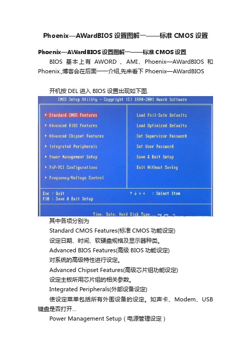
Phoenix—AWardBIOS设置图解一——标准CMOS设置Phoenix—AWardBIOS设置图解一——标准CMOS设置BIOS基本上有AWORD 、AMI、Phoenix—AWardBIOS和Phoenix.,博客会在后面一一介绍,先来看下Phoenix—AWardBIOS开机按DEL进入BIOS设置出现如下图.其中各项分别为Standard CMOS Features(标准CMOS功能设定)设定日期、时间、软硬盘规格及显示器种类。
Advanced BIOS Features(高级BIOS功能设定)对系统的高级特性进行设定。
Advanced Chipset Features(高级芯片组功能设定)设定主板所用芯片组的相关参数。
Integrated Peripherals(外部设备设定)使设定菜单包括所有外围设备的设定。
如声卡、Modem、USB 键盘是否打开...Power Management Setup(电源管理设定)设定CPU、硬盘、显示器等设备的节电功能运行方式。
PNP/PCI Configurations(即插即用/PCI参数设定)设定ISA的PnP即插即用介面及PCI介面的参数,此项仅在您系统支持PnP/PCI时才有效。
Frequency/Voltage Control(频率/电压控制)设定CPU的倍频,设定是否自动侦测CPU频率等。
Load Fail-Safe Defaults(载入最安全的缺省值)使用此菜单载入工厂默认值作为稳定的系统使用。
Load Optimized Defaults(载入高性能缺省值)使用此菜单载入最好的性能但有可能影响稳定的默认值。
Set Supervisor Password(设置超级用户密码)使用此菜单可以设置超级用户的密码。
Set User Password(设置用户密码)使用此菜单可以设置用户密码。
Save & Exit Setup(保存后退出)保存对CMOS的修改,然后退出Setup程序。
英语作文-探索集成电路设计的未来趋势与发展方向

英语作文-探索集成电路设计的未来趋势与发展方向Exploring the Future Trends and Development Directions of Integrated Circuit Design。
In recent years, the field of integrated circuit (IC) design has witnessed rapid advancements and breakthroughs. As the backbone of modern technology, ICs are essential components in various electronic devices, ranging from smartphones and computers to medical equipment and automotive systems. In this article, we will explore the future trends and development directions of IC design, focusing on three key aspects: miniaturization, power efficiency, and functional integration.First and foremost, miniaturization is a fundamental trend in IC design. Over the years, the size of ICs has continuously decreased, leading to the development of smaller and more powerful electronic devices. This trend is expected to continue in the future, with the demand for compact and portable devices on the rise. To achieve miniaturization, designers need to overcome various challenges, such as reducing power consumption, improving heat dissipation, and enhancing signal integrity. Advanced fabrication technologies, such as nanoscale lithography and 3D integration, will play a crucial role in enabling further miniaturization of ICs.Secondly, power efficiency is another important aspect of IC design. With the increasing demand for energy-saving devices and the growing concern for environmental sustainability, power efficiency has become a key consideration in IC design. Designers are constantly exploring new techniques to reduce power consumption without compromising performance. This includes the use of low-power design methodologies, such as voltage scaling, clock gating, and power gating, as well as the integration of power management circuits. Additionally, the development of energy harvesting technologies, such as solar cells and wireless charging, presents opportunities for further improving the power efficiency of ICs.Lastly, functional integration is a significant direction for the future of IC design. Traditionally, ICs were designed to perform specific functions, such as processing, memory, or communication. However, the increasing complexity of electronic systems demands higher levels of integration. Designers are now focusing on integrating multiple functions onto a single chip, leading to the development of system-on-chip (SoC) and system-in-package (SiP) solutions. This trend enables the creation of more versatile and compact devices, as well as the realization of emerging technologies like internet of things (IoT) and artificial intelligence (AI). To achieve functional integration, designers need to address challenges related to interconnectivity, power distribution, and thermal management.In conclusion, the future of IC design is characterized by miniaturization, power efficiency, and functional integration. These trends are driven by the demand for smaller, more energy-efficient, and multifunctional electronic devices. To stay at the forefront of IC design, designers need to embrace advanced fabrication technologies, explore innovative power-saving techniques, and focus on integrating multiple functions onto a single chip. By doing so, they can contribute to the development of cutting-edge technologies and shape the future of the electronics industry.。
单片机篮球计分器毕业论文中英文资料外文翻译文献

单片机篮球计分器外文翻译一英文原文:DescriptionThe AT89C51 is a low-power, high-performance CMOS 8-bit microcomputer with 4K bytes of Flash Programmable and Erasable Read Only Memory (PEROM) and 128 bytes RAM. The device is manufactured using Atmel’s high density nonvolatile memory technology and is compatible with the industry standardMCS-51™ instruction set and pinout. The chip combines a versatile 8-bit CPU with Flash on a monolithic chip, the Atmel AT89C51 is a powerful microcomputer which provides a highly flexible and cost effective solution to many embedded control applications.Features:• Compatible with MCS-51™ Products• 4K Bytes of In-System Reprogrammable Flash Memory• Endurance: 1,000 Write/Erase Cycles• Fully Static Operation: 0 Hz to 24 MHz• Th ree-Level Program Memory Lock• 128 x 8-Bit Internal RAM• 32 Programmable I/O Lines• Two 16-Bit Timer/Counters• Six Interrupt Sources• Programmable Serial Channel• Low Power Idle and Power Down ModesThe AT89C51 provides the following standard features: 4K bytes of Flash, 128 bytes of RAM, 32 I/O lines, two 16-bit timer/counters, a five vector two-level interrupt architecture, a full duplex serial port, on-chip oscillator and clock circuitry. In addition, the AT89C51 is designed with static logic for operation down to zero frequency and supports two software selectable power saving modes. The Idle Mode stops the CPU while allowing the RAM, timer/counters, serial port and interrupt system to continue functioning. The Power Down Mode saves the RAM contents but freezes the oscillator disabling all other chip functions until the next hardware reset. Pin Description:VCC Supply voltage.GND Ground.Port 0Port 0 is an 8-bit open drain bidirectional I/O port. As an output port each pin can sink eight TTL inputs. When is are written to port 0 pins, the pins can be used as high impedance inputs.Port 0 may also be configured to be the multiplexed loworder address/data bus during accesses to external program and data memory. In this mode P0 has internal pullups.Port 0 also receives the code bytes during Flash programming, and outputs the code bytes during program verification. External pullups are required during program verification.Port 1Port 1 is an 8-bit bidirectional I/O port with internal pullups. The Port 1 output buffers can sink/source four TTL inputs. When 1s are written to Port 1 pins they are pulled high by the internal pullups and can be used as inputs. As inputs, Port 1 pins that are externally being pulled low will source current (IIL) because of the internal pullups.Port 1 also receives the low-order address bytes during Flash programming and verification.Port 2Port 2 is an 8-bit bidirectional I/O port with internal pullups. The Port 2 output buffers can sink/source four TTL inputs. When 1s are written to Port 2 pins they are pulled high by the internal pullups and can be used as inputs. As inputs, Port 2 pins that are externally being pulled low will source current (IIL) because of the internal pullups.Port 2 emits the high-order address byte during fetches from external program memory and during accesses to external data memory that use 16-bit addresses (MOVX @ DPTR). In this application it uses strong internal pull-ups when emitting 1s. During accesses to external data memory that use 8-bit addresses (MOVX @ RI), Port 2 emits the contents of the P2 Special Function Register.Port 2 also receives the high-order address bits and some control signals during Flash programming and verification.Port 3Port 3 is an 8-bit bidirectional I/O port with internal pullups. The Port 3 output buffers can sink/source four TTL inputs. When 1s are written to Port 3 pins they are pulled high by the internal pullups and can be used as inputs. As inputs, Port 3 pins that are externally being pulled low will source current (IIL) because of the pullups.Port 3 also serves the functions of various special features of the AT89C51 as listed below:receives somecontrol signals forFlash programmingand verification.RSTReset input. Ahigh on this pin fortwo machine cycles while the oscillator is running resets the device.ALE/PROGAddress Latch Enable output pulse for latching the low byte of the address during accesses to external memory. This pin is also the program pulse input (PROG) during Flash programming.In normal operation ALE is emitted at a constant rate of 1/6 the oscillator frequency, and may be used for external timing or clocking purposes. Note, however, that one ALE pulse is skipped during each access to external Data Memory.If desired, ALE operation can be disabled by setting bit 0 of SFR location 8EH. With the bit set, ALE is active only during a MOVX or MOVC instruction. Otherwise, the pin is weakly pulled high. Setting the ALE-disable bit has no effect if the microcontroller is in external execution mode.PSENProgram Store Enable is the read strobe to external program memory.When the AT89C51 is executing code from external program memory, PSEN is activated twice each machine cycle, except that two PSEN activations are skipped during each access to external data memory.EA/VPPExternal Access Enable. EA must be strapped to GND in order to enable the device to fetch code from external program memory locations starting at 0000H up to FFFFH. Note, however, that if lock bit 1 is programmed, EA will be internally latched on reset.EA should be strapped to VCC for internal program executions.This pin also receives the 12-volt programming enable voltage(VPP) during Flash programming, for parts that require 12-volt VPP.XTAL1Input to the inverting oscillator amplifier and input to the internal clock operating circuit.XTAL2Output from the inverting oscillator amplifier.Oscillator CharacteristicsXTAL1 and XTAL2 are the input and output, respectively, of an invertingamplifier which can be configured for use as an on-chip oscillator, as shown in Figure1. Either a quartz crystal or ceramic resonator may be used. To drive the device from an external clock source, XTAL2 should be left unconnected while XTAL1 is driven as shown in Figure2. There are no requirements on the duty cycle of the external clock signal, since the input to the internal clocking circuitry is through adivide-by-two flip-flop, but minimum and maximum voltage high and low time specifications must be observed.Idle ModeIn idle mode, the CPU puts itself to sleep while all the onchip peripherals remain active. The mode is invoked by software. The content of the on-chip RAM and all the special functions registers remain unchanged during this mode. The idle mode can be terminated by any enabled interrupt or by a hardware reset.It should be noted that when idle is terminated by a hard ware reset, the device normally resumes program execution, from where it left off, up to two machine cycles before the internal reset algorithm takes control. On-chip hardware inhibits access to internal RAM in this event, but access to the port pins is not inhibited. To eliminate the possibility of an unexpected write to a port pin when Idle is terminated by reset, the instruction following the one that invokes Idle should not be one that writes to aport pin or to external memory.二中文翻译:AT89C51是美国ATMEL公司生产的低电压,高性能CMOS8位单片机,片内含4Kbytes的快速可擦写的只读程序存储器(PEROM)和128 bytes 的随机存取数据存储器(RAM),器件采用ATMEL公司的高密度、非易失性存储技术生产,兼容标准MCS-51产品指令系统,片内置通用8位中央处理器(CPU)和flish 存储单元,功能强大AT89C51单片机可为您提供许多高性价比的应用场合,可灵活应用于各种控制领域。
常用集成电路名词缩写

PLCC Plastic Leaded Chip Carrier
PLE Physical Layout Estimator
PLI Programming Language Interface
PLL Phase Locked Loop
POP Process Oriented Programming
PPA Performance,Power,Area
APR Auto place and route
ARM Advanced RISC Machines
ASB ASCII ASIC
Advanced System Bus
American standard code for information interchange
Application Special Integrated Circuit
DVE Discovery Visualization Environment
DVFS Dynamic Voltage Frequency Scaling
DVR Design Rule Violation
DVT Design verification test
ECC Error Correcting Code
CTL Computation tree logic
CTS Clock Tree Synthesis
DAC Digital-to-Analog Converter
DC Design compiler
DCM Digital Clock Manager
DCT Discrete cosine transform
SEB Single Event Burnout
SEE Single Event Effect
半导体物理与器件物理

半导体物理、材料、工艺 半导体器件物理 集成电路工艺 集成电路设计和测试 微系统,系统
微电子学发展的特点
向高集成度、高性能、低功耗、高可靠性电路方向发展 与其它学科互相渗透,形成新的学科领域: 光电集成、MEMS、生物芯片
半导体概要
固体材料:绝缘体、半导体、导体 (其它:半金属,超导体)
MEM
Math
Bus
Controller
IO
Graphics
PCB集成 工艺无关
系统
亚微米级工艺 依赖工艺 基于标准单元互连 主流CAD:门阵列 标准单元
集成电路芯片
世纪之交的系统设计
SYSTEM-ON-A-CHIP
深亚微米、超深亚 微米级工艺 基于IP复用 主流CAD:软硬件协 同设计
1970
1980
1990
2000
2010
存储器容量 60%/年 每三年,翻两番
1965,Gordon Moore 预测 半导体芯片上的晶体管数目每两年翻两番
1.E+9 1.E+8 1.E+7 1.E+6 1.E +5 1.E+4 1.E+3
’70 ’74 ’78 ’82 ’86 ’90 ’94 ’98 ’2002
Pentium II: 7,500,000
微处理器的性能
100 G 10 G Giga 100 M 10 M Mega Kilo
1970 1980 1990 2000 2010
Peak Advertised Performance (PAP)
Moore’s Law
Real Applied Performance (RAP) 41% Growth
英语作文-集成电路设计行业中的行业热点与前沿技术

英语作文-集成电路设计行业中的行业热点与前沿技术In the rapidly evolving field of integrated circuit (IC) design, industry focus continually shifts towards emerging trends and cutting-edge technologies that drive innovation and shape the future of electronics. Understanding these industry hotspots is crucial for professionals and enthusiasts alike to stay ahead in this dynamic landscape.One of the prominent trends in IC design is the relentless pursuit of miniaturization and increased functionality. This trend is exemplified by advancements in nanotechnology, where engineers push the boundaries of what is physically possible on a silicon chip. The ongoing development of FinFET (Fin Field-Effect Transistor) technology has been pivotal in this regard, allowing for greater transistor density and improved power efficiency compared to conventional planar transistors. As demand grows for smaller, faster, and more energy-efficient devices, manufacturers are investing heavily in techniques such as multi-patterning lithography and advanced packaging solutions to achieve these goals.Moreover, the integration of artificial intelligence (AI) into IC design workflows represents another pivotal area of development. AI techniques, particularly machine learning algorithms, are revolutionizing various aspects of design automation, from optimization and verification to layout synthesis. By harnessing vast amounts of data and computational power, AI enables designers to explore complex design spaces more effectively and shorten time-to-market for new products. This trend is expected to accelerate as AI algorithms become more sophisticated and accessible, empowering both established firms and startups to innovate rapidly.Furthermore, the relentless pursuit of energy efficiency remains a critical focal point for the IC design industry. With the proliferation of mobile devices, IoT (Internet of Things) applications, and data centers, minimizing power consumption while maintaining performance has become paramount. Innovations such as ultra-low-power designtechniques, adaptive voltage scaling, and on-chip power management units are instrumental in meeting these challenges. Additionally, emerging technologies like silicon photonics offer promising avenues for reducing power consumption in high-speed interconnects, paving the way for future generations of energy-efficient computing systems.In parallel, the industry is witnessing significant advancements in specialized IC design for niche applications. Fields such as biomedical electronics, automotive electronics, and quantum computing demand tailored solutions that go beyond traditional CMOS (Complementary Metal-Oxide-Semiconductor) technologies. These specialized ICs often require stringent reliability, low noise, and high sensitivity, prompting innovations in materials, device architectures, and fabrication techniques. As these sectors expand, they drive cross-disciplinary collaborations and inspire novel approaches to IC design that cater to specific application requirements.Looking ahead, the convergence of these trends underscores a transformative era in IC design, characterized by unprecedented levels of integration, intelligence, and efficiency. As researchers and engineers continue to push boundaries, the industry's landscape will continue to evolve, fueled by innovations that redefine what is possible with semiconductor technology. Embracing these advancements and anticipating future developments will be essential for stakeholders seeking to navigate and capitalize on the opportunities presented by the dynamic field of integrated circuit design.。
英语作文-掌握集成电路设计中的关键技术与方法

英语作文-掌握集成电路设计中的关键技术与方法Integrated Circuit (IC) design plays a pivotal role in modern electronics, serving as the foundation for virtually all electronic devices we use today. Mastering the key techniques and methods in IC design is crucial for engineers and researchers in this field. This article explores the essential aspects of IC design, highlighting the methodologies and technologies that drive innovation and efficiency in this complex discipline.### Understanding IC Design Fundamentals。
At its core, IC design involves the creation of miniature electronic circuits that integrate thousands to billions of components onto a single semiconductor chip. This integration enables devices to perform complex functions while minimizing size and power consumption. The process begins with conceptualizing the circuit's functionality and architecture, followed by detailed design and verification stages.### Key Stages in IC Design。
- 1、下载文档前请自行甄别文档内容的完整性,平台不提供额外的编辑、内容补充、找答案等附加服务。
- 2、"仅部分预览"的文档,不可在线预览部分如存在完整性等问题,可反馈申请退款(可完整预览的文档不适用该条件!)。
- 3、如文档侵犯您的权益,请联系客服反馈,我们会尽快为您处理(人工客服工作时间:9:00-18:30)。
CMOS System-on-a-Chip Voltage Scaling beyond 50nm Azeez J Bhavnagarwala, Blanca Austin, Ashok Kapoor‡ and James D Meindl Microelectronics Rsrch. Cntr. and School of Elec. and Computer Eng. , Georgia Inst. of Tech., Atlanta GA 30332‡LSI Logic Corporation, Milpitas, CA 95035Abstract†The limits on CMOS energy dissipation imposed by subthreshold leakage currents and by wiring capacitance are investigated for CMOS generations beyond 50nm at NTRS projected local and global clock rates for high performance processors. Physical short-channel MOSFET models that consider high-field effects, threshold voltage roll-off and subthreshold swing roll-up are employed in tandem with stochastic interconnect distributions to calculate optimal supply voltage, threshold voltage and gate sizes that minimize total CMOS power dissipation by exploiting trade-offs between saturation drive current and subthreshold leakage current and between device size and wiring capacitance. CMOS power dissipation at its lower limit, increases exponentially with clock frequency imposing limits on performance set by heat removal. Heat removal constraints at high local clock rates, limiting the average wire length and device size within a local zone of synchrony, or macrocell, in a short-wire cellular array architecture are used to project the maximum macrocell size and count for generations beyond 100nm.1. IntroductionThe supply voltage for future gigascale integrated systems are projected to scale to 0.37V for the 35nm, 17GHz generation [1] to reduce electric field strengths and also power dissipation (Fig. 1), increases of which are projected to be driven by higher clock rates, higher overall capacitance and larger chip sizes. A key challenge in the design of bulk Si CMOS logic circuits will be to meet the projected performances given the competing requirements of high performance and low standby power at low voltages [1,2,3] in the presence of threshold voltage reductions due to short-channel effects and subthreshold swing increases due to the 2D electrostatic charge coupling between gate and source/drain terminals of the MOSFET.A methodology [4] simultaneously considering the device, circuit and system levels of the design hierarchy and distinguishing local and global clock rates, is employed to minimize total power dissipated from a static CMOS critical path gate during a clock cycle. This methodology assumes a realistic environment of chip size, logic gate count, clock frequency, wiring capacitance, critical path depth and range of operating temperature. This analysis uses physical and stochastic models, verified by HSPICE, MEDICI and actual microprocessor implementations to investigate opportunities to scale V dd to the optimal point corresponding to the limits of CMOS power dissipation where leakage power balances switching power†This work was supported by the Defense Advanced Research Project Agency (Contract: F3361595C1623), the Semiconductor Research Corporation (SJ-374-002) and by LSI Logic Corporation dissipation, and when device capacitance balances wiring capacitance. The analysis considers Retrograde Doped (RD) (Fig.2) MOSFETs – the bulk Si alternative to a Uniformly Doped (UD) MOSFET that promises, higher performance and superior scalability [5] (Fig 3).2. Circuit and Device ModelsThe performance of a generic CMOS processor is modeled assuming a global critical path of 15 [6], 2-way NAND stages, each stage driving average wire lengths (Fig 4). Average wire lengths, in units of gate pitches, are determined (Table 1) from stochastic interconnect distributions [7], derived recursively using Rent’s rule, and verified for an actual microprocessor in Fig. 5. In logic-intensive CMOS chips, packing densities are interconnect limited [8] where the effective size of a gate is determined by its wireability [9]. The gate pitch is estimated from NTRS projections for microprocessor chip size, and logic transistor count after discounting the extrapolated increases in cache size and cache area for high performance processors (Fig 6). Assuming equal interconnect cross-sectional dimensions, and that neighboring wiring planes in a multi-level network provide an approximate ground plane, total capacitance per unit length, including fringing effects, is estimated using analytical models in [10]. Device performance is modeled using compact low-voltage Transregional MOSFET models [11,12] (Figs 7,8,9) that predict circuit performance in the sub-threshold, saturation and linear regions of operation providing continuous and smooth transitions across region boundaries. High field-effects on carrier mobility are incorporated by adopting the mobility reduction model in [13]. Smoothness and continuity of the drain current expressions in the triode, saturation and the subthreshold regions are obtained by requiring differentiability and continuity of the product of the effective mobility and the areal charge density of inversion layer carriers. Low field mobility dependence on temperature and doping concentration is estimated using empirical models reported in [14]. The doping profile for the RD structure is selected as one that yields the smallest depletion depth, corresponding to the least DIBL effects for a given V to and gate oxide thickness [15]. Increases in leakage current due to DIBL (Drain Induced Barrier Lowering) effects are calculated using 2D subthreshold models [6] that accurately predict the threshold voltage roll-off and subthreshold swing increase (Fig 10) dependence on supply voltage, device geometries and doping profile. The 2-way NAND gate, as a basic circuit building block in the critical path, has a performance that parallels that of any other circuit actually used in processor critical paths in reflecting technology improvements [16]. The improved delay dependence on fan-in at short channel lengths [17] due to a smaller reduction in the saturation drain current with a rise in the source voltage of the topmost series-connected MOSFET is modeled physically by calculating the fractional reductionof the normalized saturation drain current for the series-connected structure [18].3. Minimum Power CMOS Random Logic NetworksPower drain of a static CMOS gate is minimized by scaling the supply voltage while meeting the performance required by scaling the threshold voltage and increasing the channel widths until further decrease in threshold voltage, increases total power due to a dominating static component [3] (Figs 10, 11) and further increases in device size increase total power due to larger gate sizes [19] (Fig 12). Optimal supply voltage (Fig 13), device threshold voltage and gate sizes are calculated corresponding to a simultaneous solution at these minima (Table 2). For a given wiring load, the performance of a static CMOS gate increases asymptotically with increasing (W/L) ratios, with gate delays reaching past the knee of the asymptotic dependence of delay on channel width. for wiring capacitance less than or equal to 40% of the total load capacitance. This point corresponds to minimum power with respect to gate size where further increases in gate size increases power linearly while permitting only asymptotic reductions in supply voltage. Critical path gates clocked at high local frequencies are assumed to be only 5 stages long and drive wire lengths averaged within a macrocell of a ‘short-wire’ cellular array architecture (Fig 14). Assuming gates are sized so that wiring capacitance is 40% of the total load, the cell count (Table 3) is calculated using the stochastic interconnect distribution by imposing a maximum heat removal coefficient of 50 W/cm2 on the average wire length of the cell, calculated using the stochastic distribution. Total CMOS power increases exponentially (Fig 15) for a given generation, with increases in clock frequency due to an exponential rise in the supply voltage necessary to meet shrinking cycle times and the accompanying increases in leakage current due to threshold voltage reductions and subthreshold swing increases. The maximum heat removal coefficients of the package thus impose limits on CMOS performance.4. Summary and ConclusionsThe limits on CMOS energy dissipation shown to be imposed by static power and by wiring capacitance, are investigated using a methodology that conjointly employs physical short-channel MOSFET drain current and threshold voltage roll-off and subthreshold swing roll-up models in tandem with stochastic wiring distributions. Optimum supply voltages, device threshold voltages, and device channel widths corresponding to minimum total power are calculated out to year 2014 for local and global critical paths. These projections are consistent with technology and cycle time forecasts by the NTRS. Limits on the performance of CMOS logic circuits are shown to be imposed by total power dissipation which increases exponentially with clock frequency. Limits on the cycle time performance imposed by power dissipation are projected for the same period. Constraints imposed by NTRS projected package heat removal coefficients, permit local clock rates to apply only within a macrocell whose size and total number are calculated using the stocahstic distribution.5. References[1] The 1997 NTRS, Semiconductor Industry Association, Dec 1997[2] J D Meindl, 'Low Power Microelectronics - Retrospect and Prospect', Proceedings of the IEEE, Vol. 83, No 4 Apr 1995, pg 619.[3] J Burr and J Shott, 'A 200mV Encoder-Decoder circuit Using Stanford Ultra Low Power CMOS' ISSCC Dig Tech Papers, Feb 1994, pp 84-85.[4] A Bhavnagarwala, V. De, B Austin and J Meindl, “Circuit Techniques for Low Power CMOS GSI”, IEEE ISLPED, Aug 1996 Dig, pp 193-197[5] B Agrawal, V. De and J Meindl, “Opportunities for Scaling FET’s for Gigascale Integration”, Proceedings of the 23rd ESSDERC, Sept 1993, pp 919 – 926.[6] P E Gronowski et al, “High performance microprocessor design”, IEEE Journal of Solid State Circuits, Vol 33, No 5, pp 676-686, May 1988.[7] J Davis, V. De & J. Meindl, “A stochastic wire-length distribution for gigascale integration (GSI) – parts I & II”, IEEE Transactions on Electron Devices,Vol 45, No. 3, pp580-597, March 1998[8] R W Keyes, ''The Wire Limited Logic Chip'', IEEE JSSC, Vol SC-17, Dec 1982, pp 1232-1233[9] B Bakoglu, “Circuit Interconnections and Packaging for VLSI”, Addison Wesley, 1990[10] J Chern et al, ''Multilevel Metal Capacitance Models for CAD Design Synthesis Systems'' IEEE EDL Vol 13, No 1, Jan 1992, pg 32.[11] R Swanson & J Meindl, “Ion-Implanted Complentary MOS Transistors in Low Voltage Circuits”, IEEE JSSC, Vol. SC-7, pp. 146-153, Apr. 1972[12] B. Austin, K. Bowman, Xinghai Tang, and J. D. Meindl, "A Low Power Transregional MOSFET Model for Complete Power-Delay Analysis of CMOS Gigascale Integration (GSI)," Proc. of the 11th Annual IEEE Intl. ASIC Conf., pp. 125-129, Sept. 1998 [13] C Sodini, P Ko and J Moll, ‘The Effect of High Fields on MOS Device and Circuit Performance’, IEEE TED, Vol ED-31, No 10, October 1984, pp 1386[14] C Jacoboni et al, ‘A review of some charge transport properties in silicon’, Solid State Electronics, No 20, Vol 77, 1977[15] B Agrawal V. De and J Meindl, “Device Parameter Optimization for Reduced Short Channel Effects in Retrograde Doped MOSFETs”, IEEE TED, Vol 43, No 2, Feb 1996, pg 365 [16] G Sai Halasz, ‘Performance Trends in High-end Processors,’ Proceedings of the IEEE, Vol 83, Jan 1995, pp 20-36[17] T Sakurai & R Newton, ''Delay Models for Series Connected MOSFET Structures'' IEEE JSSC, Vol 28, No 1, Jan 1993, pg 40 [18] A Bhavnagarwala, B Austin, J Meindl, “Minimum Supply Voltage for bulk Si CMOS GSI”, IEEE ISLPED, Aug 1998 Dig, pp 100-103[19] A Chandrakasan, S Sheng and R Broderson, 'Low-Power CMOS Digital Design', IEEE JSSC Vol 27, No 4, April 1992, pp 473-484Figure 1: Historical trends with 1997 NTRS projectionsd1d0Figure 2: Shallow junctionUniform Doped (UD) andRetrograde Doped (RD)MOSFETs.Figure 3: Calculated V to roll-off for bulk Si at NTRS projected gate oxide thickness [6]Figure 8 : Comparison of 0.25micron CMOS HSPICE drain characteristics with theTransregional model (TRM).W=0.5µmFigure 7 : Comparison of 0.25micron CMOS HSPICE gate characteristics with theTransregional model (TRM).W=0.5µmFigure 4 : Subthreshold swing increases accompany threshold voltage reductions increasing stand-by currents substantiallyFigure 9 : Comparison of 0.25 micron CMOS HSPICE simulations with propagation delay models used from [4]Figure 6: Cache size extrapolations to discount SRAM cell transistors from total transistor count when calculating average wire length of a logic networkFigure 5 [7]: Stochastic wiring distribution comparison with an actual microprocessor implementation. The distribution is used to calculate the average interconnect length between two logic gatesFigure 11 &12 : Total power dissipation and its component’s dependence on supply voltage, threshold voltage and NFETchannel width. PFET channel width is calculated for equal rise and fall times.YearF(µm)Chip size,cm 2N gates ×106Cw (fF)19970.25 3.0 1.0733.419990.18 3.4 3.124.320020.13 4.39.118.120050.10 5.225.715.520080.07 6.266.712.120110.057.5177.59.420140.0359.0465.57.9Year ‘97‘99‘02‘05‘08‘11‘14F(µm).25.18.13.10.07.05.035Tox (A)453222151186f clk (GHz).75 1.2 1.6 2.0 2.5 3.0 3.7V topt (V)0.220.210.20.180.170.160.16V ddopt (V) 1.23 1.010.910.720.640.520.41−∆V TO (V)103958875543942∆S (mV/dec) 2.0 2.2 2.7 3.2 3.2 3.0 5.0P total (µW)17.114.311.48.6 6.3 4.9 3.8Table-2: Optimal V dd, V topt , W/L n,p for across-chip global clock rates.NTRS projected gate oxide thickness are assumed.Table 1: Average wiring capacitance estimates for NTRS generations using the stochastic interconnect distribution.Yr‘05‘08‘11‘14F(µm).10.07.05.035T ox (A)151186F clk (GHz) 3.5 6.010.016.9C w (fF)15.611.17.9 5.7N cells 7226611054412V ddopt 1.050.750.550.51V topt 0.190.180.160.14Table-3: Average wire lengths and wiringcapacitance imposed by heat removal for the sub-100nm generations. Size and number ofmacrocells are calculated using the stochastic wiring distribution [7] Q=50W/cm 2Figure 15: Exponential increase in power with clock frequency impose limits on CMOS performanceFigure 14: Optimal V dd and NTRS projectionsFigure 10: Physical drain current and short channelMOSFET threshold voltage roll-off models are used withstochastic interconnect distributions, toproject optimal critical path gate designsminimizing total power dissipated by CMOS logic circuits for each NTRS technology generation.L (min feature size)= 50nm f clk (local clock rate) = 10GHz t ox (gate oxide thickness) = 8 Åa (% switching activity)= 0.05b (clock skew) = 0.9n cp (logic depth) = 5C w (average wire cap)= 4.4fF f in (average fan-in) = 2f out (average fan-out) = 2T MAX (maximum temperature) = 400o K V ddopt (optimal Vdd) = 0.6V V topt (optimal Vto) = 0.17V(W/L)n (optimal NFET W/L) = 14(W/L)p (optimal PFET W/L) = 16Figure 13: A short-wire cellular array architecture with local and global clock frequencies where local clocks apply only within the boundary of a macrocell。