CM100TU-24H中文资料
IGBT的型号,参数,及价格总结

43
CT 15SM-24
15A/1200V IGBT单管
CT 35SM-8
200A/400V IGBT单管
41
CT 75AM-12
75A/600V IGBT单管
78
三菱型号(1U 600V) IGBT
技术指标
批价(元)
三菱型号(1U 600V) IGBT
技术指标
批价(元)
400A/1200V/1U
1150
1MBI 200F-120
200A/1200V/1U
655
1MBI 400NN-120
400A/1200V/1U
1150
1MBI 300F-120
300A/1200V/1U
880
1MBI 400L(N)(S)-120
400A/1200V/1U
1150
1MBI 300L(N)(S)-120
200A/1200V/2U
930/1030
CM 150E3Y(E3U)-24E
150A/1400V/2U
880/960
CM 300DY(DU)-24(E)
300A/1200V/2U
1630/1580
CM 200E3Y(E3U)-24E
200A/1400V/2U
1080/1210
CM 50DY-28H
300A/600V/2U
780/880
CM 300E3Y(E3U)-12E
300A/600V/2U
960/1080
CM 400DY(DU)-12H(E)
400A/600V/2U
1455
型号2U
(1200/1400V) IGBT
CM300DU-24NFH中文资料

Gate-emitter threshold voltage Thermal resistance *1Collector-emitter voltage Gate-emitter voltage Maximum collector dissipation Maximum collector dissipation Junction temperature Storage temperature Isolation voltage WeightV CE = V CES , V GE = 0V V GE = V GES , V CE = 0V T j = 25°CT j = 125°C V CC = 600V, I C = 300A, V GE = 15V V CC = 600V, I C = 300A V GE1 = V GE2 = 15VR G = 1Ω, Inductive load switching operation I E = 300AI E = 300A, V GE = 0V IGBT part (1/2 module)FWDi part (1/2 module)Case to fin, Thermal compound Applied *2 (1/2 module)IGBT part (1/2 module)FWDi part (1/2 module)I C = 30mA, V CE = 10VI C = 300A, V GE = 15VV CE = 10V V GE = 0V1200±2030060030060011301900–40 ~ +150–40 ~ +12525003.5 ~ 4.53.5 ~ 4.5400HIGH POWER SWITCHING USEV V A A A A W W °C °C V N • m N • m g116.5—4740.9—30080500150250—3.50.110.18—0.066*30.1*310mA µA nF nF nF nC ns ns ns ns µC V °C/W °C/W °C/W °C/W °C/W Ω——5.05.0———1360—————13———0.04———————————————————————16V V 4.57.5ns Collector cutoff current Gate leakage current Collector-emittersaturation voltage (Note 4)Input capacitance Output capacitanceReverse transfer capacitance Total gate charge Turn-on delay time Turn-on rise time Turn-off delay time Turn-off fall timeReverse recovery time Reverse recovery charge Emitter-collector voltage Contact thermal resistance Thermal resistance *4External gate resistanceI CES I GES C ies C oes C res Q G t d(on)t rt d(off)t ft rr (Note 1)Q rr (Note 1)V EC(Note 1)R th(j-c)Q R th(j-c)R R th(c-f)R th(j-c’)Q R th(j-c’)R R GSymbol ParameterV GE(th)V CE(sat)*1 : T C measured point is shown in page OUTLINE DRAWING.*2 : Typical value is measured by using Shin-etsu Silicone “G-746”.*3 : If you use this value, R th(f-a) should be measured just under the chips.*4 : T C ’ measured point is just under the chips.Note 1. I E , V EC , t rr & Q rr represent characteristics of the anti-parallel, emitter to collector free-wheel diode (FWDi).2. Pulse width and repetition rate should be such that the device junction temp. (T j ) does not exceed T jmax rating.3. Junction temperature (T j ) should not increase beyond 150°C.4. No short circuit capability is designed.G-E Short C-E Short Operation (Note 2)Pulse (Note 2)Operation (Note 2)Pulse(Note 2)T C = 25°C T C ’ = 25°C *4Main Terminal to base plate, AC 1 min.Main Terminal M6Mounting holes M6Typical valueSymbol ParameterCollector current Emitter currentMounting torque ConditionsUnit Ratings V CES V GES I C I CMI E (Note 1)I EM (Note 1)P C (Note 3)P C ’ (Note 3)T j T stg V iso———Unit Typ.Limits Min.Max.Test conditionsMAXIMUM RATINGS (Tj = 25°C)ELECTRICAL CHARACTERISTICS (Tj = 25°C)HIGH POWER SWITCHING USEHIGH POWER SWITCHING USE。
IGBT型号大全一览

IGBT型号大全一览型号(1U 1200V )技术指标型号(1U 1700V) 技术指标BSM200GA120DN2 200A/1200V/1U BSM200GA170DN2 200A/1700V/1U BSM300GA120DN2 300A/1200V/1U BSM300GA170DN2 300A/1700V/1U BSM400GA120DN2 400A/1200V/1U BSM400GA170DLC 400A/1700V/1U BSM200GA120DLC 200A/1200V/1U BSM200GA170DLC 200A/1700V/1U BSM300GA120DLC 300A/1200V/1U BSM300GA170DLC 300A/1700V/1U BSM400GA120DLC 400A/1200V/1U型号2U/600/1200/1700V )技术指标型号(2U 1200V/1700V) 技术指标BSM50GB60DLC 50A/600V/2U BSM75GB170DN2 75A/1700V/2UBSM75GB60DLC 75A/600V/2U BSM100GB170DN2 100A/1700V/2UBSM100GB60DLC 100A/600V/2U BSM150GB170DN2 150A/1700V/2U BSM150GB60DLC 150A/600V/2U BSM200GB170DLC 200A/1700V/2U BSM200GB60DLC 200A/600V/2U BSM25GAL120DN2 25A/1200V/2U BSM300GB60DLC 300A/600V/2U BSM50GAL120DN2 50A/1200V/2U BSM25GB120DN2 25A/1200V/2U BSM75GAL120DN2 75A/1200V/2UBSM35GB120DN2 35A/1200V/2U BSM100GAL120DN2 100A/1200V/2U BSM50GB120DN2 50A/1200V/2U BSM150GAL120DN2 150A/1200V/2U BSM75GB120DN2 75A/1200V/2U BSM200GAL120DN2 200A/1200V/2U BSM100GB120DN2K 100A/1200V/2U BSM300GAL120DN2 300A/1200V/2U BSM35GB120DLC 35A/1200V/2U BSM100GAL120DLCK 100A/1200V/2U BSM50GB120DLC 50A/1200V/2U BSM150GAL120DLC 150A/1200V/2U BSM75GB120DLC 75A/1200V/2U BSM200GAL120DLC 200A/1200V/2U BSM150GB170DLC 150A/1700V/2U BSM300GAL120DLC 300A/1200V/2U BSM100GB120DN2 100A/1200V/2U BSM75GAR120DN2 75A/1200V/2U BSM150GB120DN2 150A/1200V/2U BSM100GAR120DN2 100A/1200V/2U BSM200GB120DN2 200A/1200V/2U BSM150GAR120DN2 150A/1200V/2U BSM300GB120DN2 300A/1200V/2U BSM200GAR120DN2 200A/1200V/2U BSM100GB120(DLC 100A/1200V/2U BSM200GB120DLC 200A/1200V/2U BSM150GB120DLC 150A/1200V/2U BSM300GB120DLC 300A/1200V/2U BSM50GB170DN2 50A/1700V/2U BSM300GAR120DN2 300A/1200V/2U BSM100GB120DLCK 100A/100V/2U型号6U /600V/1200V 技术指标型号(6U /1200V/1700V) 技术指标BSM10GD60DLC 10A/600V/6U BSM25GD120DN2 25A/1200V/6UBSM15GD60DLC 15A/600V/6U BSM25GD120D2 25A/1200V/6UBSM25GD60DLC 25A/600V/6U BSM35GD120DN2 35A/1200V/6UBSM30GD60DLC 30A/600V/6U BSM35GD120D2 35A/1200V/6UBSM50GD60DLC 50A/600V/6U BSM50GD120DN2 50A/1200V/6UBSM75GD60DLC 75A/600V/6U BSM75GD120DN2 75A/1200V/6UBSM100GD60DLC 100A/600V/6U BSM50GD120DLC 50A/1200V/6UBSM100GD120DN2 100A/1200V/6U BSM75GD120DLC 75A/1200V/6U BSM100GD120DLC 100A/1200V/6U BSM35GD120DLC 35A/1200V/6UBSM150GD60DLC 150A/600V/6U BSM50GD170DL 50A/1700V/6UBSM200GD60DLC 200A/600V/6U BSM75GD170DL 75A/1700V/6UBSM10GD120DN2 10A/1200V/6U BSM100GT170DL 100A/1700V/6U BSM15GD120D2 15A/1200V/6U BSM100GT120DN2 100A/1200V/6UBSM15GD120DN1 15A/1200V/6U BSM150GT120DN2 150A/1200V/6U BSM15GD120DN2 15A/1200V/6U BSM150GT170DL 150A/1700V/6U BSM25GD120DN1 25A/1200V/6U BSM200GT120DN2 200A/1200V/6U 二.欧派克超大功率EUPEC IGBT 模块( 1200V/1600V/2500V/3300V 系列) 型号( 1 单元) 技术指标型号(1 单元) 技术指标FZ200R12KF2 200A/1200V/1U FZ1200R12KF4 1200A/1200V/1UFZ300R12KF2 300A/1200V/1U FZ1200R16KF4 1200A/1600V/1UFZ400R12KF2 400A/1200V/1U FZ1200R25KF1 1200A/2500V/1UFZ800R12KF4 800A/1200V/1U FZ1200R25KF4 1200A/2500V/1UFZ800R16KF4 800A/1600V/1U FZ1200R33KF1 1200A/3300V/1UFZ800R33KF1 800A/3300V/1U FZ1600R12KF4 1600A/1200V/1UFZ900R16KF1 900A/1600V/1U FZ1800R12KF4 1800A/1200V/1UFZ1000R12KF4 1000A/1200V/1U FZ1800R16KF4 1800A/1600V/1UFZ2400R12KF4 2400A/1200V/1U型号( 2 单元) 技术指标型号( 2 单元) 技术指标FZ200R33KF2 200A/3300V/2U FZ600R12KF4 600A/1200V/2UFZ400R12KF4 400A/1200V/2U FZ600R16KF4 600A/1600V/2UFZ400R16KF4 400A/1600V/2U FZ800R12KF4 800A/1200V/2UFZ400R33KF1 400A/3300V/2U FZ800R17KF6B2 800A/1700V/2UFZ400R33KF2 400A/3300V/2U型号( 6 单元) 技术指标型号( 6 单元) 技术指标FS300R12KF4 300A/1200V/6U FS400R12KF4 400A/1200V/6UFS300R16KF4 300A/1600V/6UFF600R12KF4FF200R33KF2 FF400R16KF4FF400R12KF4 FF400R33KF1FF400R33KF2 FF800R12KF4FF600R16KF4 FF800R17KF6B2三.西门康SEMIKRON,IGBT 模块型号( 1U 1200V) 技术指标型号(1U /1700V) 技术指标SKM200GA123D 200A/1200V/1U SKM400GA173D 400A/1700V/1USKM300GA123D 300A/1200V/1U SKM300GA173D 400A/1700V/1USKM400GA123D 400A/1200V/1U SKM500GA174D 500A/1700V/1USKM500GA123D 500A/1200V/1U SKM500GA124D 500A/1200V/1USKM600GA124D 600A/1200V/1U型号( 2U/1200V/1700V ) 技术指标型号(2U /1200V/1700V) 技术指标SKM50GB123D 50A/1200V/2U SKM145GAL123D 145A/1200V/2USKM75GB123D 75A/1200V/2U SKM150GAL123D 150A/1200V/2USKM100GB123D 100A/1200V/2U SKM200GAL123D 200A/1200V/2U SKM145GB123D 145A/1200V/2U SKM300GAL123D 300A/1200V/2USKM150GB123D 150A/1200V/2U SKM400GAL124D 400A/1200V/2USKM200GB123D 200A/1200V/2U SKM100GAL173D 100A/1700V/2USKM300GB123D 300A/1200V/2U SKM145GAL174DN 145A/1700V/2USKM400GB123D 400A/1200V/2U SKM200GAL173D 200A/1700V/2USKM75GB124D 75A/1200V/2U SKM200GAL125D 200A/1200V/2USKM100GB124D 100A/1200V/2U SKM400GAL125D 400A/1200V/2USKM145GB124D 145A/1200V/2U SKM300GB124D 300A/1200V/2USKM150GB124D 150A/1200V/2U SKM400GB124D 400A/1200V/2USKM200GB124D 200A/1200V/2U SKM200GB174D 200A/1700V/2USKM75GB173D 75A/1700V/2U SKM200GAR173D 200A/1700V/2USKM100GB173D 100A/1700V/2U SKM75GAR123D 75A/1200V/2USKM150GB173D 150A/1700V/2U SKM100GAR123D 100A/1200V/2USKM145GB174DN 145A/1700V/2U SKM145GAR123D 145A/1200V/2USKM200GB173D 200A/1700V/2U SKM150GAR123D 150A/1200V/2USKM300GB174D 300A/1700V/2U SKM200GAR123D 200A/1200V/2USKM50GAL123D 50A/1200V/2U SKM300GAR123D 300A/1200V/2USKM75GAL123D 75A/1200V/2U SKM400GAR124D 400A/1200V/2USKM100GAL123D 100A/1200V/2U SKM145GAL124D 145A/1200V/2U型号( 6U 1200V ) 技术指标型号(6U 1200V) 技术指标SKM22GD123D 22A/1200V/6U SKM75GD123D 75A/1200V/6USKM40GD123D 40A/1200V/6U SKM100GD123D 100A/1200V/6USKM40GD124D 40A/1200V/6U SKM75GD124D 75A/1200V/6U四.三菱MITSUBISHI IGBT模块+单管IGBT(TO—220、TO—3P)(耐压600/1200/1400/1700/2500/3300V)型号技术指标型号(IGBT 单管) 技术指标CT60AM-20 60A/1000V IGBT单管CT75SM-12CT30SM-12 30A/600V IGBT单管CT15SM-24 15A/1200V IGBT单管CT35SM-8 200A/400V IGBT单管CT75AM-12 75A/600V IGBT单管型号技术指标型号技术指标CM300HA-12H 300A/600V/1U CM200HA-24H 200A/1200V/1UCM400HA-12H 400A/600V/1U CM300HA-24H 300A/1200V/1UCM600HA-12H 600A/600V/1U CM400HA-24H 400A/1200V/1UCM600HU-12H 600A/600V/1U CM600HA-24H 600A/1200V/1UCM400HU-24H 400A/1200V/1U CM600HU-24H 600A/1200V/1UCM200HU-24H 200A/1200V/1U CM800HA-24H 800A/1200V/1UCM300HU-24H 300A/1200V/1U CM1000HA-24H 1000A/1200V/1UCM300HA-12E 300A/600V/1U CM200HA-24E 200A/1200V/1UCM400HA-12E 400A/600V/1U CM300HA-24E 300A/1200V/1UCM600HA-12E 600A/600V/1U CM400HA-24E 400A/1200V/1UCM600HU-12E 600A/600V/1U CM600HA-24E 600A/1200V/1UCM400HU-24E 400A/1200V/1U CM600HU-24E 600A/1200V/1UCM200HU-24E 200A/1200V/1U CM800HA-24E 800A/1200V/1UCM300HU-24E 300A/1200V/1U CM1000HA-24E 1000A/1200V/1U型号技术指标型号技术指标CM400HA-28H 400A/1400V/1U CM800HA-50H 800A/2500V/1UCM600HA-28H 600A/1400V/1U CM1200HA-50H 1200A/2500V/1U CM1000HA-28H 1000A/1400V/1U CM800HA-66H 800A/3300V/1U CM400HA-34H 400A/1700V/1U CM1200HA-66H 1200A/3300V/1U CM800HD-66H 800A/3300V/1U CM800HD-50H 800A/2500V/1UCM1200HD-66H 1200A/3300V/1U CM1200HD-50H 1200A/2500V/1U 型号技术指标型号技术指标CM50DY-12H 50A/600V/2U CM50E3Y-12E 50A/600V/2UCM75DY-12H 75A/600V/2U CM75E3Y-12E 75A/600V/2UCM100DY-12H 100A/600V/2U CM100E3Y-12E 100A/600V/2UCM150DY-12H 150A/600V/2U CM150E3Y-12E 150A/600V/2UCM200DY-12H 200A/600V/2U CM200E3Y-12E 200A/600V/2UCM300DY-12H 300A/600V/2U CM300E3Y-12E 300A/600V/2UCM400DY-12H 400A/600V/2U CM50E3U-12E 50A/600V/2UCM75DU-12H 75A/600V/2U CM75E3U-12E 75A/600V/2UCM100DU-12H 100A/600V/2U CM100E3U-12E 100A/600V/2UCM150DU-12H 150A/600V/2U CM150E3U-12E 150A/600V/2UCM200DU-12H 200A/600V/2U CM200E3U-12E 200A/600V/2UCM300DU-12H 300A/600V/2U CM300E3U-12E 300A/600V/2UCM400DU-12H 400A/600V/2U CM75DU-12E 75A/600V/2UCM50DY-12E 50A/600V/2U CM100DU-12E 100A/600V/2UCM75DY-12E 75A/600V/2U CM150DU-12E 150A/600V/2UCM100DY-12E 100A/600V/2U CM200DU-12E 200A/600V/2UCM150DY-12E 150A/600V/2U CM300DU-12E 300A/600V/2UCM200DY-12E 200A/600V/2U CM400DU-12E 400A/600V/2UCM300DY-12E 300A/600V/2U CM400DY-12E 400A/600V/2U型号技术指标型号技术指标CM50DY-24H 50A/1200V/2U CM300DY-28H 300A/1400V/2UCM75DY-24H 75A/1200V/2U CM50E3Y-24E 50A/1200V/2UCM100DY-24H 100A/1200V/2U CM75E3Y-24E 75A/1200V/2UCM150DY-24H 150A/1200V/2U CM100E3Y-24E 100A/1200V/2U CM200DY-24H 200A/1200V/2U CM150E3Y-24E 150A/1200V/2U CM300DY-24H 300A/1200V/2U CM200E3Y-24E 200A/1200V/2U CM50DU-24H 50A/1200V/2U CM50E3U-24E 50A/1200V/2UCM75DU-24H 75A/1200V/2U CM75E3U-24E 75A/1200V/2UCM100DU-24H 100A/1200V/2U CM100E3U-24E 100A/1200V/2U CM150DU-24H 150A/1200V/2U CM150E3U-24E 150A/1200V/2U CM200DU-24H 200A/1200V/2U CM200E3U-24E 200A/1200V/2U CM300DU-24H 300A/1200V/2U CM300E3Y-24E 300A/1200V/2U CM50DY-24E 50A/1200V/2U CM50DU-24E 50A/1200V/2UCM75DY-24E 75A/1200V/2U CM75DU-24E 75A/1200V/2UCM100DY-24E 100A/1200V/2U CM100DU-24E 100A/1200V/2UCM150DY-24E 150A/1200V/2U CM150DU-24E 150A/1200V/2UCM200DY-24E 200A/1200V/2U CM200DU-24E 200A/1200V/2UCM300DY-24E 300A/1200V/2U CM300DU-24E 300A/1200V/2UCM50DY-28H 50A/1400V/2U CM300E3U-24E 300A/1200V/2UCM75DY-28H 75A/1400V/2U CM400DY-50H 400A/2500V/2UCM200DY-28H 200A/1400V/2U CM400DY-66H 400A/3300V/2U型号技术指标型号技术指标CM15TF-12H 15A/600V/6U CM15TF-24H 15A/1200V/6UCM20TF-12H 20A/600V/6U CM20TF-24H 20A/1200V/6UCM30TF-12H 30A/600V/6U CM30TF-24H 30A/1200V/6UCM50TF-12H 50A/600V/6U CM50TF-24H 50A/1200V/6UCM75TF-12H 75A/600V/6U CM75TF-24H 75A/1200V/6UCM100TF-12H 100A/600V/6U CM100TF-24H 100A/1200V/6UCM150TF-12H 150A/600V/6U CM50TF-28H 50A/1400V/6UCM75TU-12H 75A/600V/6U CM50TU-24H 50A/1200V/6UCM100TU-12H 100A/600V/6U CM75TU-24H 75A/1200V/6UCM150TU-12H 150A/600V/6U CM100TU-24H 100A/1200V/6UCM15TF-12E 15A/600V/6U CM15TF-24E 15A/1200V/6UCM20TF-12E 20A/600V/6U CM20TF-24E 20A/1200V/6UCM30TF-12E 30A/600V/6U CM30TF-24E 30A/1200V/6UCM50TF-12E 50A/600V/6U CM50TF-24E 50A/1200V/6UCM75TF-12E 75A/600V/6U CM75TF-24E 75A/1200V/6UCM100TF-12E 100A/600V/6U CM100TF-24E 100A/1200V/6UCM150TF-12E 150A/600V/6U CM50TU-24E 50A/1200V/6UCM75TU-12E 75A/600V/6U CM75TU-24E 75A/1200V/6UCM100TU-12E 100A/600V/6U CM100TU-24E 100A/1200V/6UCM150TU-12E 150A/600V/6U CM50TF-28H 50A/1400V/6UCM200TU-12H 200A/600V/6U CM75TF-28H 75A/1400V/6UCM100TF-28H 100A/1400V/6U五.富士Fuji IGBT 模块( 耐压600V/1200V/1400V/1800V/2000V 系列) 型号( 1U 600V ) 技术指标型号(1U 600V) 技术指标1MBH60D-100 60A/1000V IGBT单管1MBI200NK-060 200A/600V/1U1MBI30L-060 30A/600V/1U 1MBI300L-060 300A/600V/1U1MBI50L-060 50A/600V/1U 1MBI300N-060 300A/600V/1U1MBI75L-060 75A/600V/1U 1MBI300F-060 300A/600V/1U1MBI100L-060 100A/600V/1U 1MBI400F-060 400A/600V/1U1MBI150NH-060 150A/600V/1U 1MBI400L-060 400A/600V/1U1MBI400N-060 400A/600V/1U 1MBI600LP-060 600A/600V/1U1MBI150NK-060 150A/600V/1U 1MBI600LN-060 600A/600V/1U1MBI200NH-060 200A/600V/1U 1MBI600NP-060 600A/600V/1U1MBI600NN-060 600A/600V/1U型号(1U 1200V ) 技术指标型号(1U 1200V) 技术指标1MBI200L-120 200A/1200V/1U 1MBI400NP-120 400A/1200V/1U1MBI200N-120 200A/1200V/1U 1MBI200S-120 200A/1200V/1U1MBI200F-120 200A/1200V/1U 1MBI400NN-120 400A/1200V/1U1MBI300F-120 300A/1200V/1U 1MBI400L-120 400A/1200V/1U1MBI300L-120 300A/1200V/1U 1MBI600PX-120 600A/1200V/1U1MBI300N-120 300A/1200V/1U 1MBI300S-120 300A/1200V/1U1MBI300JN-120 300A/1200V/1U 型号(1U1400/1800/2000V) 技术指标1MBI300JB-120 300A/1200V/1U 1MBI600PX-140 600A/1400V/1U1MBI300NP-120 300A/1200V/1U 1MBI800PN-180 800A/1800V/1U1MBI300NN-120 300A/1200V/1U 1MBI400L-200 400A/2000V/1U型号( 2U 600V) 技术指标型号(2U 600V) 技术指标2MBI50L-060 50A/600V/2U 2MBI200LB-060 200A/600V/2U2MBI75L-060 75A/600V/2U 2MBI300L-060 300A/600V/2U2MBI100L-060 100A/600V/2U 2MBI300LB-060 300A/600V/2U2MBI150L-060 150A/600V/2U 2MBI300NK-060 300A/600V/2U2MBI150LB-060 150A/600V/2U 2MBI300NK-060 300A/600V/2U2MBI150NK-060 150A/600V/2U 2MBI400NK-060 400A/600V/2U2MBI50F-060 50A/600V/2U 2MBI200KB-060 200A/600V/2U2MBI75F-060 75A/600V/2U 2MBI300F-060 300A/600V/2U2MBI100F-060 100A/600V/2U 2MBI300KB-060 300A/600V/2U2MBI150F-060 150A/600V/2U 2MBI300NB-060 300A/600V/2U2MBI150KB-060 150A/600V/2U 2MBI400NR-060 400A/600V/2U2MBI150NC-060 150A/600V/2U 2MBI300N-060 300A/600V/2U2MBI50N-060 50A/600V/2U 2MBI150N-060 150A/600V/2U2MBI75N-060 75A/600V/2U 2MBI200N-060 200A/600V/2U2MBI100N-060 100A/600V/2U 2MB400N-060 400A/600V/2U2MB400L-060 400A/600V/2U 2MBI600NT-060 600A/600V/2U2MBI200NR-060 200A/600V/2U 2MBI200F-060 200A/600V/2U2MBI200NK-060 200A/600V/2U 2MBI400L-060 400A/600V/2U2MBI400N-060 400A/600V/2U 2MBI200L-060 200A/600V/2U型号( 2U 1400V ) 技术指标型号(2U 1400V) 技术指标2MBI25L-120 25A/1200V/2U 2MBI150L-120 150A/1200V/2U2MBI50L-120 50A/1200V/2U 2MBI150NB-120 150A/1200V/2U2MBI75L-120 75A/1200V/2U 2MBI150NT-120 150A/1200V/2U2MBI100L-120 100A/1200V/2U 2MBI200L-120 200A/1200V/2U2MBI75SC-120 75A/1200V/2U 2MBI150F-120 150A/1200V/2U2MBI150SC-120 150A/1200V/2U 2MBI150N-120 150A/1200V/2U2MBI50N-120 50A/1200V/2U 2MBI150NC-120 200A/1200V/2U2MBI75N-120 75A/1200V/2U 2MBI150NT-120 300A/1200V/2U2MBI100F-120 100A/1200V/2U 2MBI200N-120 200A/1200V/2U2MBI100N-120 100A/1200V/2U 2MBI75P-140 75A/1400V/2U2MBI50P-140 50A/1400V/2U 2MBI200PB-140 200A/1400V/2U2MBI100PC-140 100A/1400V/2U 2MBI300P-140 300A/1400V/2U2MBI150PC-140 150A/1400V/2U 2MBI100SC-120 100A/1200V/2U2MBI100NC-120 100A/1200V/2U 2MBI100NB-120 100A/1200V/2U2MBI200S-120 200A/1200V/2U 2MBI200NF120 200A/1200V/2U2MBI300L-120 300A/1200V/2U 2MBI200NB-120 200A/1200V/2U型号( 6U 600V ) 技术指标型号(6U 600V) 技术指标6MBI10L-060 10A/600V/6U 6MBI60FA-060 60A/600V/6U6MBI15L-060 15A/600V/6U 6MBI75L-060 75A/600V/6U6MBI10F-060 10A/600V/6U 6MBI10N-060 10A/600V/6U6MBI15F-060 15A/600V/6U 6MBI75F-060 75A/600V/6U6MBI15N-060 15A/600V/6U 6MBI75N-060 75A/600V/6U6MBI15LS-060 15A/600V/6U 6MBI75FA-060 75A/600V/6U6MBI20L-060 20A/600V/6U 6MBI100L-060 100A/600V/6U6MBI30L-060 30A/600V/6U 6MBI100FA-060 100A/600V/6U6MBI20F-060 20A/600V/6U 6MBI100F-060 100A/600V/6U6MBI30F-060 30A/600V/6U 6MBI30N-060 30A/600V/6U6MBI30FA-060 30A/600V/6U 6MBI150FB-060 150A/600V/6U6MBI50L-060 50A/600V/6U 6MBI200FB-060 200A/600V/6U6MBI50F-060 50A/600V/6U 6MBI50N-060 50A/600V/6U6MBI50FA-060 50A/600V/6U 6MBI50J-060 50A/600V/6U6MBI100J-060 100A/600V/6U型号( 6U 1200V ) 技术指标型号(6U 1200V) 技术指标6MBI8L-120 8A/1200V/6U 6MBI15S-120 15A/1200V/6U6MBI8F-120 8A/1200V/6U 6MBI8N-120 8A/1200V/6U6MBI15L-120 15A/1200V/6U 6MBI25S-120 25A/1200V/6U6MBI25L-120 25A/1200V/6U 6MBI35S-120 35A/1200V/6U6MBI25LB-120 25A/1200/6U 6MBI50S-120 50A/1200V/6U6MBI50L-120 50A/1200V/6U 6MBI75S-120 75A/1200V/6U6MBI50F-120 50A/1200V/6U 6MBI50N-120 50A/1200V/6U6MBI15F-120 15A/1200V/6U 6MBI15N-120 15A/1200V/6U6MBI25F-120 25A/1200V/6U 6MBI25N-120 25A/1200V/6U6MBI50J-120 50A/1200V/6U 6MBI100S-120 100A/1200V/6U富士IGBT 六单元,小型单列直插式封装,体积小,价格低,特别适用于家用电器变频控制UPS、AC/DC伺服系统等。
CM1002中文资料

CM1000, 1500, 2500, 3500 SERIESHIGH CURRENT SILICON BRIDGE RECTIFIERSVOLTAGE - 50 to 800 VoltsCURRENT - 10 to 35 AmperesRecongnized File #E111753FEATURESl Electrically Isolated Metal Case for Maximum Heat Dissipation l Surge Overload Ratings to 400 Amperesl These bridges are on the U/LRecognized Products List forcurrents of 10, 25 and 35 amperes MECHANICAL DA TACase: Metal, electrically isolated Terminals: Plated .25” FASTON or wire Lead £r 40 mils Weight: 1 ounce, 30 grams Mounting position: AnyMACXIMUM RA TINGS AND ELECTRICAL CHARACTERISTICSRating at 25¢J ambient temperature unless otherwise specified.Single phase, half wave, 60Hz, resistive or inductive load.For capacitive load, derate current by 20%.-00-01-02-04-06-08UNITS Max Recurrent Peak Reverse Voltage 50100200400600800V Max RMS Input Voltage 3570140280420560V Max DC Blocking Voltage50100200400600800V CM1010A CM1515A CM2525A Max Average Forward Current*for Resistive Load at TC=55¢J CM3535A CM10200A CM15300A CM25300A Non-repetitive Peak Forward Surge Current at Rated Load CM35400A CM10 5A CM15 I F 7.5A CM25 12.5AMax Forward Voltage per Bridge Element at Specified Current CM35 17.5A 1.2VMax Reverse Leakage Current at Rated DC Blocking Voltage10£g A CM10CM15 / CM35I 2t Rating for fusing ( t < 8.3ms )CM25374 / 664A 2sTypical Thermal Resistance (Fig. 3) R £c JC 2.5¢J /W Operating Temperature Range T J Storage Temperature Range T STG -55 to +150¢JNOTES:* Unit mounted on metal heat-sinkCM-25 CM-25WRATING AND CHARACTERISTIC CURVES CM1000 THRU CM35001000100101.0VFM VOLTS PEAKCASE TEMPERATURE T C ¢JFig. 1-TYPICAL INSTANTANEOUS FORWARDCHARACTERISTICS AT T J = 25¢J Fig. 2-OUTPUT CURRENT VS. CASE TEMPERATURERESISTIVE OR INDUCTIVE LOAD T J = 150¢J25 40 60 80 100 120 140 160 180AMBIENT TEMPERATURE, T A ¢JAVERAGE OUTPUT CURRENT, AMPERESFig. 3-OUTPUT CURRENT VS. AMBIENT TEMPERATURE RESISTIVE OR INDUCTIVE LOAD BRIDGE MOUNTED ON A 8"×8" ALUMINUM PLATE 25"THICKFig. 4-POWER DISSIPATION VS. AVERAGE OUTPUT CURRENT RESISTIVE OR INDUCTI VE LOAD, T J = 150¢J。
CM100DC-24NFM中文资料

TENTATIVECM100DC-24NFMPre. S.Kawabata,H.Takemoto,M.HiyoshiApr. Y.Nagashima 1-Dec-'06 RevHIGH POWER SWITCHING USE─────────────────────────────────────────────────── Notice: This is not a final specification. Some parametric limits are subject to change.CM100DC-24NFMI C ・・・・・・・・・・・・・・・・・・・・・・・・・・・・ 100A V CES ・・・・・・・・・・・・・・・・・・・・・・・・ 1200V Insulated Type2-elements in a pack Caution: No short circuit capability is designed.APPLICATIONHigh frequency switching use & Resonant inverter power supply, etcABSOLUTE MAXIMUM RATINGS (T j =25°C, unless otherwise specified) Symbol Item Conditions Ratings Units V CES Collector-emitter voltage G-E Short 1200 V V GES Gate-emitter voltage C-E Short ± 20 V I C Operation 100I CM Collector current Pulse *4200 A I E *3 Operation 100I EM *3 Emitter current Pulse *4 200 AP C *5 Maximum collector dissipation T C =25°C *1 670 W T j Junction temperature - 40 ~ +150°C T stg Storage temperature - 40 ~ +125°C V iso Isolation voltage Main terminal to base plate, AC 1 min. 2500 V- Torque strength Main terminal M6 3.5 ~ 4.5 N ・m - Torque strength Mounting holes M6 3.5 ~ 4.5 N ・m - Weight Typical value 375 g────────────────────────────────────────────────── ELECTRICAL CHARACTERISTICS (T j =25°C, unless otherwise specified) Symbol Item Conditions Min. Typ. Max.Units I CES Collector cutoff currentV CE =V CES , V GE =0V - - 1 mAV GE(th) Gate-emitterthreshold voltage I C =10mA, V CE =10V 4.5 6.0 7.5 VI GES Gate leakage current ±V GE =V GES , V CE =0V - - 0.5 μAI C =100A *6 T j =25°C - 3.0 4.5V CE(sat)Collector to emitter saturationvoltageV GE =15V T j =125°C - 3.0 -VC ies Input capacitance - - 16 C oes Output capacitance V GE =0V, V CE =10V *6 - - 1.3 nF C res Reverse transfer capacitance--0.3Q G Total gate charge V CC =600V, I C =100A, V GE =15V - 450 - nC t d(on) Turn-on delay time V CC =600V, I C =100A - - 100t r Turn-on rise timeV GE1=V GE2=15V, R G =3.1Ω - - 50t d(off) Turn-off delay time Inductive load - - 250t fTurn-off fall time switching operation - 60 200t rr *3 Reverse recovery time I E =100A - 70 120ns Q rr *3 Reverse recovery charge - 6 -μC V EC *3 Emitter-collector voltage I E =100A, V GE =0V - 2.0 3.0 V R th(j-c)Q IGBT part (1/2 module) *1 - - 0.186R th(j-c)RThermal resistanceFWDi part (1/2 module) *1 - - 0.28R th(c-f) Contact thermal resistance Case to fin, Thermal grease applied (1/2module) *1 *2- 0.02 -°C/W R G External gate resistance 3.1 - 31 Ω*1: T C , T f measured point is just under the chips.*2: Typical value is measured by using Shin-Etsu Chemical Co.,Ltd "G-747".*3: I E , I EM , V EC , t rr & Q rr represent characteristics of the anti-parallel, emitter to collector free-wheel diode (FWDi).*4: Pulse width and repetition rate should be such that the device junction temperature (T j ) dose not exceed Tjmax rating.*5: Junction temperature (T j ) should not increase beyond 150°C.*6: Pulse width and repetition rate should be such as to cause neglible temperature rise.──────────────────────────────────────────────────OUTLINE DRAWINGDimensions in mmCIRCUIT DIAGRAM。
RSS100N03中文资料
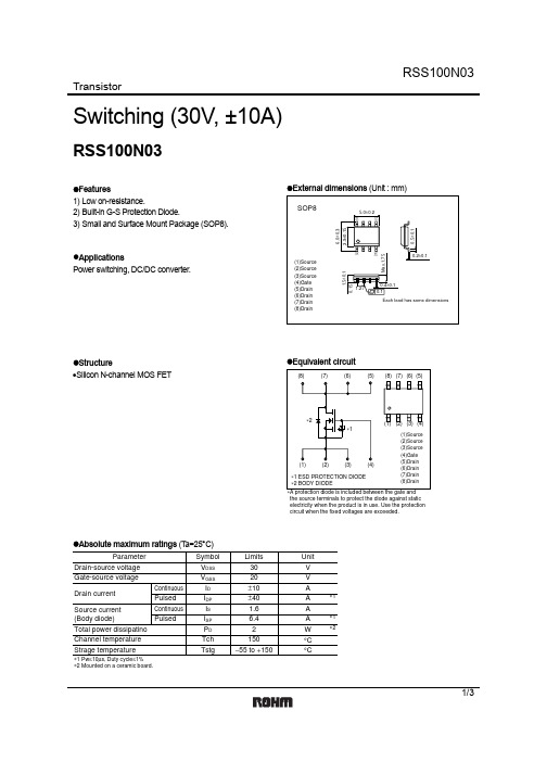
Transistor1/3Switching (30V, ±10A)RSS100N03z Features1) Low on-resistance.2) Built-in G-S Protection Diode.3) Small and Surface Mount Package (SOP8).z ApplicationsPower switching, DC/DC converter.z External dimensions (Unit : mm)z Structure•Silicon N-channel MOS FET z Equivalent circuitthe source terminals to protect the diode against static electricity when the product is in use. Use the protection circuit when the fixed voltages are exceeded.z Absolute maximum ratings (T a=25°C)∗1∗1∗2ParameterV V DSS Symbol 30V V GSS 20A I D ±10A I DP ±40A I S 1.6A I SP 6.4W P D 2°C Tch 150°CTstg −55 to +150Limits Unit Drain-source voltage Gate-source voltage Drain current Total power dissipatino Channel temperature Strage temperatureContinuous Pulsed Continuous Source current (Body diode)Pulsed∗1 Pw ≤10µs, Duty cycle ≤1%∗2 Mounted on a ceramic board.Transistor2/3z Thermal resistance (T a=25°C)°C / WRth (ch-a)62.5ParameterSymbol Limits Unit Channel to ambient∗ Mounted on a ceramic board.∗z Electrical characteristics (T a=25°C)z Body diode characteristics (Source-Drain Characteristics) (T a=25°C)Forward voltageV SD −− 1.2V I S=6.4A, V GS =0VParameterSymbol Min.Typ.Max.Unit Conditions∗Pulsed∗z Electrical characteristic curvesDRAIN-SOURCE VOLTAGE : V DS (V)C A P A C I T A N C E : C (p F )Fig.1 Typical Capacitancevs. Drain-Source VoltageDRAIN CURRENT : I D (A)S W I T C H I N G T I M E : t (n s )Fig.2 Switching CharacteristicsTOTAL GATE CHARGE : Qg (nC)G A T E -S O U R C E V O L T A G E : V G S (V )Fig.3 Dynamic Input CharacteristicsTransistor3/3GATE-SOURCE VOLTAGE : V GS (V)D R A I N C U R RE N T : I D (A )Fig.4 Typical Transfer CharacteristicsGATE-SOURCE VOLTAGE : V GS (V)S T A T I C D R A I N -S O U R C E O N -S T A T E R E S I S T A N C E : R D S (o n ) (m Ω)Fig.5 Static Drain-SourceOn-State Resistance vs. Gate-Source VoltageSOURCE-DRAIN VOLTAGE : V SD (V)S O U R C E C U R R E N T : I s (A )Fig.6 Source Current vs.Source-Drain VoltageDRAIN CURRENT : I D (A)1101001000S T A T I C D R A I N -S O U R C E O N -S T A T E R E S I S TA N C E : R D S (o n ) (m Ω)Fig.7 Static Drain-SourceOn-State Resistance vs. Drain Current (Ι)DRAIN CURRENT : I D (A)S T A T I C D R A I N -S O U R C E O N -S T A T E R E S I S T A N C E : R D S (o n ) (m Ω)Fig.8 Static Drain-SourceOn-State Resistance vs. Drain Current (ΙΙ)DRAIN CURRENT : I D (A)S T A T I C D R A I N -S O U R C E O N -S T A T E R E S I S T A N C E : R D S (o n ) (m Ω)Fig.9 Static Drain-SourceOn-State Resistance vs. Drain Current (ΙΙΙ)AppendixAbout Export Control Order in JapanProducts described herein are the objects of controlled goods in Annex 1 (Item 16) of Export Trade ControlOrder in Japan.In case of export from Japan, please confirm if it applies to "objective" criteria or an "informed" (by MITI clause)on the basis of "catch all controls for Non-Proliferation of Weapons of Mass Destruction.Appendix1-Rev1.0。
三菱IGBT模块CM100MXA-24S说明书

MITSUBISHI IGBT MODULESCM100MXA-24SHIGH POWER SWITCHING USEINSULATED TYPECM100MXA-24S- 6th Generation NX series -Collector current I C ............................... 100A Collector-emitter voltage V CES .. (1200V)●Flat base Type●Copper base plate (non-plating)●Tin plating pin terminals●RoHS Directive compliantCIB (Converter+Inverter+BrakeCopper ) ●UL Recognized under UL1557, File E323585APPLICATIONAC Motor Control, Motion/Servo Control, Power supply, etc. OUTLINE DRAWING & INTERNAL CONNECTIONTERMINALt=0.8SECTION ATolerance otherwise specified Division of DimensionTolerance 0.5 to 3 ±0.2 over 3 to 6 ±0.3 over 6 to 30 ±0.5 over 30 to 120 ±0.8 over 120 to 400 ±1.2INTERNAL CONNECTIONP1(48~49) N1(44~45)GUP(13)U(14~15)GUN(40)TH1(29)GVP(18)V(19~20)GVN(33)GWP(23)W(24~25)GWN(31)B(52~53)GB(41)N T CClampDiP(54~56) N(59~61) R(1~2) S(5~6) T(9~10)The tolerance of size between terminals is assumed to be ±0.4.INSULATED TYPEABSOLUTE MAXIMUM RATINGS (T j =25 °C, unless otherwise specified)Inverter part IGBT/FWDiSymbol Item ConditionsRating Unit V CES Collector-emitter voltage G-E short-circuited 1200 V V GESGate-emitter voltageC-E short-circuited±20VI C DC, T C =119 °C (Note.2, 4)100I CRM Collector current Pulse (Note.3)200 A P t o t Total power dissipationT C =25 °C (Note.2, 4) 750 WI E (Note.1) T C =25 °C (Note.2, 4)100I ERM(Note.1)Emitter currentPulse (Note.3)200 AT j m a xMaximum junction temperature-175°CBrake part IGBT/ClampDiSymbol Item ConditionsRating Unit V CES Collector-emitter voltage G-E short-circuited 1200 V V GESGate-emitter voltageC-E short-circuited±20VI C DC, T C =125 °C (Note.2)50I CRM Collector current Pulse (Note.3)100 A P t o t Total power dissipationT C =25 °C (Note.2, 4)425 WV RRM Repetitive peak reverse voltage G-E short-circuited1200VI F (Note.1)T C =25 °C (Note.2, 4)50I FRM(Note.1)Forward currentPulse (Note.3)100 AT j m a xMaximum junction temperature-175°CConverter part ConvDiSymbol Item ConditionsRating Unit V RRM Repetitive peak reverse voltage - 1600 V E a Recommended AC input voltage RMS440VI O DC output current 3-phase full wave rectifying, T C =125 °C (Note.2)100 AThe sine half wave 1 cycle peak value, I FSM Surge forward current f=60 Hz, non-repetitive1000 A I 2t Current square timeValue for one cycle of surge current 4165 A 2s T j m a xMaximum junction temperature-150°CModuleSymbol Item ConditionsRating Unit T C m a x Maximum case temperature (Note.2)125 °CT j o p Operating junction temperature - -40 ~ +150 T s t g Storage temperature --40 ~ +125 °C V i s o lIsolation voltageTerminals to base plate, RMS, f=60 Hz, AC 1 min2500VMECHANICAL CHARACTERISTICSLimitsSymbol Item Conditions Min. Typ. Max. UnitM sMounting torqueMounting to heat sink M 5 screw2.53.0 3.5 N·m Terminal to terminal6.47 - - d s Creepage distance Terminal to base plate 14.27 - - mm Terminal to terminal 6.47 - - d a Clearance Terminal to base plate 12.33--mmm Weight -- 300 - ge cFlatness of base plateOn the centerline X, Y(Note.5)±0 - +100 μmINSULATED TYPEELECTRICAL CHARACTERISTICS (T j =25 °C, unless otherwise specified) Inverter part IGBT/FWDiLimitsSymbol Item Conditions Min. Typ. Max. UnitI C ES Collector-emitter cut-off current V CE =V CES , G-E short-circuited - - 1 mAI G ES Gate-emitter leakage current V GE =V GES , C-E short-circuited - - 0.5 μAV G E(th) Gate-emitter threshold voltage I C =10 mA, V CE =10 V 5.4 6.0 6.6 VT j =25 °C - 1.80 2.25 T j =125 °C - 2.00 - V C Es at (Terminal) Collector-emitter saturation voltageI C =100 A (Note.6),V GE =15 V T j =150 °C - 2.05 - V T j =25 °C - 1.70 2.15 T j =125 °C - 1.90 - V C Es at (Chip)Collector-emitter saturation voltageI C =100 A (Note.6) ,V GE =15 VT j =150 °C- 1.95-V C i e s Input capacitance - - 10C o e s Output capacitance -- 2.0 C r e s Reverse transfer capacitance V CE =10 V, G-E short-circuited- - 0.17 nFQ G Gate charge V CC =600 V, I C =100 A, V GE =15 V - 233 - nC t d (o n ) Turn-on delay time --300t r Rise time V CC =600 V, I C =100 A, V GE =±15 V, - - 200t d (o f f )Turn-off delay time- - 600 t f Fall time R G =6.2 Ω, Inductive load - - 300 nsT j =25 °C - 1.8 2.25 T j =125 °C - 1.8 - V EC(Note.1)(Terminal) Emitter-collector voltageI E =100 A(Note.6),G-E short-circuited T j =150 °C - 1.8 - VT j =25 °C - 1.7 2.15 T j =125 °C - 1.7 - V EC(Note.1)(Chip) Emitter-collector voltage I E =100 A(Note.6),G-E short-circuitedT j =150 °C- 1.7 - V t r r(Note.1)Reverse recovery timeV CC =600 V, I E =100 A, V GE =±15 V, - - 300 nsQ r r(Note.1)Reverse recovery chargeR G =6.2 Ω, Inductive load - 5.3 - μC E on Turn-on switching energy per pulse V CC =600 V, I C =I E =100 A,- 8.6 - E of f Turn-off switching energy per pulse V GE =±15 V, R G =6.2 Ω, T j =150 °C, - 10.7 - mJ E r r(Note.1)Reverse recovery energy per pulse Inductive load-10.2-mJMain terminals-chip, per switch,R C C '+EE' Internal lead resistance T C =25 °C (Note.2)- - 3.5 m Ω r gInternal gate resistancePer switch--ΩBrake part IGBT/ClampDiLimits Symbol Item Conditions Min. Typ. Max. UnitI C ES Collector-emitter cut-off current V CE =V CES , G-E short-circuited - - 1 mAI G ES Gate-emitter leakage current V GE =V GES , C-E short-circuited - - 0.5 μAV G E(th) Gate-emitter threshold voltage I C =5 mA, V CE =10 V 5.4 6.0 6.6 VT j =25 °C - 1.80 2.25 T j =125 °C - 2.00 - V C Es at (Terminal) Collector-emitter saturation voltageI C =50 A(Note.6),V GE =15 V T j =150 °C - 2.05 - V T j =25 °C - 1.70 2.15 T j =125 °C - 1.90 - V C Es at (Chip)Collector-emitter saturation voltageI C =50 A(Note.6),V GE =15 VT j =150 °C- 1.95-V C i e s Input capacitance - - 5.1C o e s Output capacitance -- 0.45C r e sReverse transfer capacitanceV CE =10 V, G-E short-circuited- - 0.1nFQ G Gate chargeV CC =600 V, I C =50 A, V GE =15V - 117 - nCINSULATED TYPEELECTRICAL CHARACTERISTICS (cont., T j =25 °C, unless otherwise specified)Brake part IGBT/ClampDiLimitsSymbol Item Conditions Min. Typ. Max. Unitt d (o n ) Turn-on delay time --300t r Rise time V CC =600 V, I C =50 A, V GE =±15 V, - - 200t d (o f f ) Turn-off delay time- - 600 t f Fall timeR G =13 Ω, Inductive load - - 300 nsI RRM Repetitive peak reverse current V R =V RRM , G-E short-circuited - - 1 mAT j =25 °C - 1.8 2.25 T j =125 °C - 1.8 - V F(Terminal) Forward voltageI F =50 A(Note.6),G-E short-circuited T j =150 °C - 1.8 - VT j =25 °C - 1.7 2.15 T j =125 °C - 1.7 - V F(Chip) Forward voltage I F =50 A(Note.6),G-E short-circuitedT j =150 °C- 1.7 - V t r r Reverse recovery time V CC =600 V, I F =50 A, V GE =±15 V, - - 300 nsQ r r Reverse recovery chargeR G =13 Ω, Inductive load - 2.7 - μC E on Turn-on switching energy per pulse V CC =600 V, I C =I F =50 A,- 5.5 - E of f Turn-off switching energy per pulse V GE =±15 V, R G =13 Ω, T j =150 °C, - 5.3 - mJ E r r Reverse recovery energy per pulse Inductive load - 4.5 - mJ r gInternal gate resistance---ΩConverter part ConvDiLimitsSymbol Item Conditions Min. Typ. Max. UnitI RRM Repetitive peak reverse currentV R =V RRM , T j =150 °C --20mAV F(Terminal)Forward voltageI F =100 A(Note.6)- 1.28 1.8 VNTC thermistor partLimitsSymbol Item Conditions Min. Typ. Max. UnitR 25 Zero power resistance T C =25 °C(Note.2)4.855.00 5.15 k ΩΔR/R Deviation of resistance T C =100 °C, R 100=493 Ω -7.3 - +7.8 % B (25/50)B constantApproximate by equation (Note.7)- 3375 - KP 25 Power dissipation T C =25 °C(Note.2)- - 10 mWTHERMAL RESISTANCE CHARACTERISTICSLimitsSymbol Item Conditions Min. Typ. Max. UnitR t h (j -c )Q Junction to case, per Inverter IGBT - - 0.20 R t h (j -c )D Junction to case, per Inverter FWDi- - 0.29 K/W R t h (j -c )Q Junction to case, per Brake IGBT - - 0.35 R t h (j -c )D Junction to case, per Brake ClampDi - - 0.63 K/W R t h (j -c )D Thermal resistance(Note. 2)Junction to case, per ConvDi--0.24K/WCase to heat sink, per 1 module,R t h (c -s )Contact thermal resistance(Note. 2)Thermal grease applied(Note.8)- 15 - K/kWINSULATED TYPENote.1: Represent ratings and characteristics of the anti-parallel, emitter-collector free wheeling diode (FWDi).Note.2: Case temperature (T C ) and heat sink temperature (T s ) are defined on the each surface (mounting side) of base plateand heat sink just under the chips. Refer to the figure of chip location.Note.3: Pulse width and repetition rate should be such that the device junction temperature (T j ) dose not exceed T j m a x rating. Note.4: Junction temperature (T j ) should not increase beyond T j m a x rating.Note.5: The base plate (mounting side) flatness measurement points (X, Y) are as follows of the following figure.-:Concavemounting sideNote.6: Pulse width and repetition rate should be such as to cause negligible temperature rise.Refer to the figure of test circuit.Note.7: )T T /()R R ln(B )/(50255025502511-=,R 25: resistance at absolute temperature T 25 [K]; T 25=25 [°C]+273.15=298.15 [K] R 50: resistance at absolute temperature T 50 [K]; T 50=50 [°C]+273.15=323.15 [K]Note.8: Typical value is measured by using thermally conductive grease of λ=0.9 W/(m·K).Note.9: Japan Electronics and Information Technology Industries Association (JEITA) standards,"EIAJ ED-4701/300: Environmental and endurance test methods for semiconductor devices (Stress test I)"Note.10: Use the following screws when mounting the printed circuit board (PCB) on the stand offs."M2.6×10 or M2.6×12 self tapping screw"The length of the screw depends on the thickness of the PCB.RECOMMENDED OPERATING CONDITIONS (T a =25 °C)LimitsSymbol Item Conditions Min. Typ. Max. UnitV C C DC supply voltage Applied across P1-N1 terminals -600850VApplied across GB-Es/V GEon Gate-emitter drive voltage G*P-*/G*N-Es (*=U,V,W) terminals 13.5 15.0 16.5 V Inverter IGBT 6.2 - 62 R G External gate resistancePer switchBrake IGBT13-130ΩINSULATED TYPECHIP LOCATION (top view)Dimension in mm, Tolerance: ±1 mmTr*P/Tr*N/TrBr: IGBT, Di*P/Di*N: FWDi (*=U/V/W), DiBr: ClampDi, CR*P/CR*N: ConvDi (*=R/S/T), Th: NTC thermistorEach mark points the center position of each chip or device.TEST CIRCUIT AND WAVEFORMSCCi Et r r , Q r r test waveformTurn-on / Turn-off switching energy and Reverse recovery energy test waveforms (Integral time instruction drawing)INSULATED TYPE TEST CIRCUITV GEV GEV GEV GEV GEV GEV GEG-Eshort-circuited GVP-V, GVN-Es,GWP-W, GWN-Es,GB-EsG-Eshort-circuitedGUP-U, GUN-Es,GWP-W, GWN-Es,GB-EsG-Eshort-circuitedGUP-U, GUN-Es,GVP-V, GVN-Es,GB-EsG-Eshort-circuitedGUP-U, GUN-Es,GVP-V, GVN-Es,GWP-W, GWN-EsUP / UN IGBT VP / VN IGBT WP / WN IGBT Brake IGBT / ClampDiV CEsat / ClampDi V F test circuitG-Eshort-circuited GVP-V, GVN-Es,GWP-W, GWN-Es,GB-EsG-Eshort-circuitedGUP-U, GUN-Es,GWP-W, GWN-Es,GB-EsG-Eshort-circuitedGUP-U, GUN-Es,GVP-V, GVN-Es,GB-EsUP / UN FWDi VP / VN FWDi WP / WN FWDi ConvDi (ex. phase-R)V EC / ConvDi V F test circuit* In case of the above example, P1/N1/U/V/W should use all each three pin terminals for the external wiring.INSULATED TYPEPERFORMANCE CURVESINVERTER PARTOUTPUT CHARACTERISTICS (TYPICAL) COLLECTOR-EMITTER SATURATION VOLTAGECHARACTERISTICS(TYPICAL)T j =25 °C(Chip)V GE =15 V(Chip)C O L L E C T O R C U R R E N T I C (A )C O L L E C T O R -E M I T T E RS A T U R A T I O N V O L T A G E V C E (V )00.511.522.533.550100150200COLLECTOR CURRENT I C (A)FREE WHEELING DIODEFORWARD CHARACTERISTICS(TYPICAL)G-E short-circuited(Chip)C O L L E C T O R -E M I T T E RS A T U R A T I O N V O L T A G E V C E (V )68101214161820E M I T T E R C U R R E N T I E (A )11010010000.511.522.53GATE-EMITTER VOLTAGE V GE (V) EMITTER-COLLECTOR VOLTAGE V EC (V)INSULATED TYPEHALF-BRIDGE SWITCHING CHARACTERISTICS (TYPICAL) HALF-BRIDGESWITCHING CHARACTERISTICS(TYPICAL)V CC =600 V, V GE =±15 V, R G =6.2 Ω, ---------------: T j =150 °C, - - - - -: T j =125 °CV CC =600 V, V GE =±15 V, I C =100 A, ---------------: T j =150 °C, - - - - -: T j =125 °C S W I T C H I N G T I M E (n s )S W I T C H I N G T I M E (n s)C GHALF-BRIDGE SWITCHING CHARACTERISTICS (TYPICAL) HALF-BRIDGESWITCHING CHARACTERISTICS(TYPICAL)V CC =600 V, V GE =±15 V, R G =6.2 Ω, ---------------: T j =150 °C, - - - - -: T j =125 °CV CC =600 V, V GE =±15 V, I C =100 A, ---------------: T j =150 °C, - - - - -: T j =125 °C S W I T C H I N G E N E R G Y (m J )R E V E R S E R E C O V E R Y E N E R G Y (m J )S W I T C H I N G E N E R G Y (m J ) R E V E R S E R E C O V E R Y E N E R G Y (m J )C EMITTER CURRENT I E (A)GINSULATED TYPECAPACITANCE CHARACTERISTICS (TYPICAL) FREE WHEELING DIODEREVERSE RECOVERY CHARACTERISTICS(TYPICAL)G-E short-circuited, T j =25 °CV CC =600 V, V GE =±15 V, R G =6.2 Ω,---------------: T j =150 °C, - - - - -: T j =125 °C C A P A C I T A N C E (n F )0.010.11101000.1110100t r r (n s ), I r r (A )COLLECTOR-EMITTER VOLTAGE V CE (V) EMITTER CURRENT I E (A)GATE CHARGE CHARACTERISTICS (TYPICAL) TRANSIENT THERMAL IMPEDANCECHARACTERISTICS(MAXIMUM)V CC =600 V, I C =100 A, T j =25 °CSingle pulse, T C =25 °CG A T E -E M I T T E R V O L T A G E V G E (V )05101520100200300400N O R M A L I Z E D T R A N S I E N T T H E R M A L R E S I S T A N C EZ t h (j -c )0.0010.010.110.000010.00010.0010.010.1110R th(j-c)Q =0.20 K/W, R th(j-c)D =0.29 K/WGATE CHARGE Q G (nC)TIME (S)INSULATED TYPEBRAKE PARTCOLLECTOR-EMITTER SATURATION VOLTAGE CHARACTERISTICS (TYPICAL) CLAMP DIODEFORWARD CHARACTERISTICS(TYPICAL)V GE =15 V(Chip)G-E short-circuited(Chip)C O L L E C T O R -E M I T T E RS A T U R A T I O N V O L T A G E V C E s a t (V )00.511.522.533.520406080100F O R W A R D V O L T AG E V F (V )110100COLLECTOR CURRENT I C (A) FORWARD CURRENT I F (A)HALF-BRIDGE SWITCHING CHARACTERISTICS (TYPICAL) HALF-BRIDGESWITCHING CHARACTERISTICS(TYPICAL)V CC =600 V, V GE =±15 V, R G =13 Ω, INDUCTIVE LOAD ---------------: T j =150 °C, - - - - -: T j =125 °CV CC =600 V, I C =50 A, V GE =±15 V, INDUCTIVE LOAD---------------: T j =150 °C, - - - - -: T j =125 °C S W I T C H I N G T I M E (n s )S W I T C H I N G T I M E (n s )COLLECTOR CURRENT I C (A) EXTERNAL GATE RESISTANCE R G (Ω)INSULATED TYPEHALF-BRIDGE SWITCHING CHARACTERISTICS (TYPICAL) HALF-BRIDGESWITCHING CHARACTERISTICS(TYPICAL)V CC =600 V, V GE =±15 V, R G =13 Ω, INDUCTIVE LOAD, PER PULSE ---------------: T j =150 °C, - - - - -: T j =125 °CV CC =600 V, I C /I F =50 A, V GE =±15 V, INDUCTIVE LOAD, PER PULSE ---------------: T j =150 °C, - - - - -: T j =125 °C S W I T C H I N G E N E R G Y (m J )R E V E R S E R E C O V E R Y E N E R G Y (m J )S W I T C H I N G EN E R G Y (m J ) R EV E R S E R E C O V E R Y E N E R G Y (m J )COLLECTOR CURRENT I C (A) FORWARD CURRENT I F (A)EXTERNAL GATE RESISTANCE R G (Ω)CLAMP DIODE REVERSE RECOVERY CHARACTERISTICS (TYPICAL) TRANSIENT THERMAL IMPEDANCECHARACTERISTICS(MAXIMUM)V CC =600 V, V GE =±15 V, R G =13 Ω, INDUCTIVE LOAD---------------: T j =150 °C, - - - - -: T j =125 °CSingle pulse, T C =25 °C t r r (n s ), I r r (A )N O R M A L I Z E D T R A N S I E N T T H E R M A L R E S I S T A N C EZ t h (j -c )0.0010.010.110.000010.00010.0010.010.1110R th(j-c)Q =0.35K/W, R th(j-c)D =0.63 K/WFORWARD CURRENT I F (A)TIME (S)INSULATED TYPECONVERTER PARTCONVERTER DIODE FORWARD CHARACTERISTICS (TYPICAL) TRANSIENT THERMAL IMPEDANCE CHARACTERISTICS(MAXIMUM)Single pulse, T C =25 °CF O R W A R D C U R R E N T I F (A )10100N O R M A L I Z E D T R A N S I E N T T H E R M A L R E S I S T A N C EZ t h (j -c )0.0010.010.110.000010.00010.0010.010.1110R th(j-c)D =0.24 K/WFORWARD VOLTAGE V F (V)TIME (S)INSULATED TYPEKeep safety first in your circuit designs!•Mitsubishi Electric Corporation puts the maximum effort into making semiconductor products better and more reliable, but there is always the possibility that trouble may occur with them. Trouble with semiconductors may lead to personal injury, fire or property damage.Remember to give due consideration to safety when making your circuit designs, with appropriate measures such as (i) placement of substitutive, auxiliary circuits, (ii) use of non-flammable material or (iii) prevention against any malfunction or mishap.Notes regarding these materials•These materials are intended as a reference to assist our customers in the selection of the Mitsubishi semiconductor product best suited to the customer's application; they do not convey any license under any intellectual property rights, or any other rights, belonging to Mitsubishi Electric Corporation or a third party.•Mitsubishi Electric Corporation assumes no responsibility for any damage, or infringement of any third-party's rights, originating in the use of any product data, diagrams, charts, programs, algorithms, or circuit application examples contained in these materials.•All information contained in these materials, including product data, diagrams, charts, programs and algorithms represents information on products at the time of publication of these materials, and are subject to change by Mitsubishi Electric Corporation without notice due to product improvements or other reasons. It is therefore recommended that customers contact Mitsubishi Electric Corporation or an authorized Mitsubishi Semiconductor product distributor for the latest product information before purchasing a product listed herein. The information described here may contain technical inaccuracies or typographical errors. Mitsubishi Electric Corporation assumes no responsibility for any damage, liability, or other loss rising from these inaccuracies or errors.Please also pay attention to information published by Mitsubishi Electric Corporation by various means, including the Mitsubishi Semiconductor home page (/Global/index.html).•When using any or all of the information contained in these materials, including product data, diagrams, charts, programs, and algorithms, please be sure to evaluate all information as a total system before making a final decision on the applicability of the information and products. Mitsubishi Electric Corporation assumes no responsibility for any damage, liability or other loss resulting from the information contained herein.•Mitsubishi Electric Corporation semiconductors are not designed or manufactured for use in a device or system that is used under circumstances in which human life is potentially at stake. Please contact Mitsubishi Electric Corporation or an authorized Mitsubishi Semiconductor product distributor when considering the use of a product contained herein for any specific purposes, such as apparatus or systems for transportation, vehicular, medical, aerospace, nuclear, or undersea repeater use.•The prior written approval of Mitsubishi Electric Corporation is necessary to reprint or reproduce in whole or in part these materials. •If these products or technologies are subject to the Japanese export control restrictions, they must be exported under a license from the Japanese government and cannot be imported into a country other than the approved destination.Any diversion or reexport contrary to the export control laws and regulations of Japan and/or the country of destination is prohibited. •Please contact Mitsubishi Electric Corporation or an authorized Mitsubishi Semiconductor product distributor for further details on these materials or the products contained therein.。
SMP100-xxxH225中文资料

®
SMP100-xxx SMP100-xxxH225
TRISIL TM
FEATURES BIDIRECTIONAL CROWBAR PROTECTION VOLTAGE RANGE : FROM 8V to 320V REPETITIVE PEAK PULSE CURRENT: IPP = 100 A (10/1000 µs) HOLDING CURRENT: IH = 150mA or 225mA LOW LEAKAGE CURRENT: IR = 2 µA max DESCRIPTION The SMP100 series are transient surge arrestors used for the protection of sensitive telecom equipment. MAIN APPLICATIONS Any sensitive equipment requiring protection against lightning strikes : ANALOG AND DIGITAL LINE CARDS MAIN DISTRIBUTION FRAMES TERMINALS AND TRANSMISSION EQUIPMENT GAS-TUBE REPLACEMENT BENEFITS NO AGEING AND NO NOISE IF DESTROYED, THE SMP100 FALLS INTO SHORT CIRCUIT,STILLENSURINGPROTECTION BOARD SPACE SAVING COMPLIES WITH THE FOLLOWING STANDARDS: CCITT K20 VDE0433 VDE0878 IEC-1000-4-5 FCC Part 68, lightning surge type A FCC Part 68, lightning surge type B BELLCORE TR-NWT-001089 First level BELLCORE TR-NWT-001089 Second level CNET l31-24
- 1、下载文档前请自行甄别文档内容的完整性,平台不提供额外的编辑、内容补充、找答案等附加服务。
- 2、"仅部分预览"的文档,不可在线预览部分如存在完整性等问题,可反馈申请退款(可完整预览的文档不适用该条件!)。
- 3、如文档侵犯您的权益,请联系客服反馈,我们会尽快为您处理(人工客服工作时间:9:00-18:30)。
Static Electrical Characteristics, Tj = 25 °C unless otherwise specified
Characteristics Collector-Cutoff Current Gate Leakage Voltage Gate-Emitter Threshold Voltage Collector-Emitter Saturation Voltage Symbol ICES IGES VGE(th) VCE(sat) QG VEC Test Conditions VCE = VCES, VGE = 0V VGE = VGES, VCE = 0V IC = 10mA, VCE = 10V IC = 100A, VGE = 15V, Tj = 25°C IC = 100A, VGE = 15V, Tj = 125°C Total Gate Charge Emitter-Collector Voltage* VCC = 600V, IC = 100A, VGE = 15V IE = 100A, VGE = 0V Min. – – 4.5 – – – – Typ. – – 6 2.9 2.85 375 – Max. 1 0.5 7.5 3.7 – – 3.2 Units mA µA Volts Volts Volts nC Volts
D C
GwP EwP GuN EuN GvN EvN
TC Measured Point
u v
TC Measured M Point GwN EwN
w
N 5 - M5 NUTS E H J E J H E
K
TAB#110 t=0.5
P Q
Description: Mitsubishi IGBT Modules are designed for use in switching applications. Each module consists of six IGBTs in a three phase bridge configuration, with each transistor having a reverse-connected superfast recovery free-wheel diode. All components and interconnects are isolated from the heat sinking baseplate, offering simplified system assembly and thermal management. Features: Low Drive Power Low VCE(sat) Discrete Super-Fast Recovery Free-Wheel Diode High Frequency Operation Isolated Baseplate for Easy Heat Sinking Applications: AC Motor Control Motion/Servo Control UPS Welding Power Supplies
0 0 4 8 12 16 20 0 40 80 120 160 200
GATE-EMITTER VOLTAGE, VGE, (VOLTS) COLLECTOR-CURRENT, IC, (AMPERES)
COLLECTOR-EMITTER SATURATION VOLTAGE CHARACTERISTICS (TYPICAL)
* Pulse width and repetition rate should be such that the device junction temperature (Tj) does not exceed Tj(max) rating.
Dynamic Electrical Characteristics, Tj = 25 °C unless otherwise specified
* Pulse width and repetition rate should be such that the device junction temperature (Tj) does not exceed Tj(max) rating. **Represents characteristics of the anti-parallel, emitter-to-collector free-wheel diode (FWDi).
Ordering Information: Example: Select the complete module number you desire from the table - i.e. CM100TU-24H is a 1200V (VCES), 100 Ampere SixIGBT Module.
Sep.1998
元器件交易网
MITSUBISHI IGBT MODULES
CM100TU-24H
HIGH POWER SWITCHING USE INSULATED TYPE
OUTPUT CHARACTERISTICS (TYPICAL)
TRANSFER CHARACTERISTICS (TYPICAL)
Diode Reverse Recovery Time Diode Reverse Recovery Charge
Thermal and Mechanical Characteristics, Tj = 25 °C unless otherwise specified
Characteristics Thermal Resistance, Junction to Case Thermal Resistance, Junction to Case Contact Thermal Resistance Symbol Rth(j-c)Q Rth(j-c)D Rth(c-f) Test Conditions Per IGBT 1/6 Module Per Free-Wheel Diode 1/6 Module Per Module, Thermal Grease Applied Min. – – – Typ. – – 0.015 Max. 0.19 0.35 – Units °C/W °C/W °C/W
Ratings Junction Temperature Storage Temperature Collector-Emitter Voltage (G-E SHORT) Gate-Emitter Voltage (C-E SHORT) Collector Current (Tc = 25°C) Peak Collector Current (Tj ≤ 150°C) Emitter Current** Peak Emitter Current** Maximum Collector Dissipation (Tj < 150°C) Mounting Torque, M5 Main Terminal Mounting Torque, M5 Mounting Weight Isolation Voltage (Main Terminal to Baseplate, AC 1 min.) Symbol Tj Tstg VCES VGES IC ICM IE IEM Pc – – – Viso CM100TU-24H -40 to 150 -40 to 125 1200 ±20 100 200* 100 200* 650 2.5~3.5 2.5~3.5 680 2500 Units °C °C Volts Volts Amperes Amperes Amperes Amperes Watts N·m N·m Grams Vrms
Type CM Current Rating Amperes 100 VCES Volts (x 50) 24
Sep.1998
元器件交易网
MITSUBISHI IGBT MODULES
CM100TU-24H
HIGH POWER SWITCHING USE INSULATED TYPE Absolute Maximum Ratings, Tj = 25 °C unless otherwise specified
元器件交易网
MITSUBISHI IGBT MODULES
CM100TU-24H
HIGH POWER SWITCHING USE INSULATED TYPE
A B F G E H E H G E S K R 4 - Mounting Holes
L GuP EuP GvP EvP
COLLECTOR-EMITTER SATURATION VOLTAGE CHARACTERISTICS (TYPICAL)
200
COLLECTOR CURRENT, IC, (AMPERES) COLLECTOR CURRENT, IC, (AMPERES)
200 160
COLLECTOR-EMITTER SATURATION VOLTAGE, VCE(sat), (VOLTS)
Characteristics Input Capacitance Output Capacitance Reverse Transfer Capacitance Resistive Load Switch Times Turn-on Delay Time Rise Time Turn-off Delay Time Fall Time Symbol Cies Coes Cres td(on) tr td(off) tf trr Qrr VCC = 600V, IC = 100A, VGE1 = VGE2 = 15V, RG = 3.1Ω, Resistive Load Switching Operation IE = 100A, diE/dt = -200A/µs IE = 100A, diE/dt = -200A/µs VCE = 10V, VGE = 0V Test Conditions Min. – – – – – – – – – Typ. – – – – – – – – 0.55 Max. 15 5 3 100 200 300 350 300 – Units nF nF nF ns ns ns ns µC µC