0.18μm CMOS and beyond-1
毕业设计论文:PLL锁相环电路
1摘 要随着通信及电子系统的飞速发展,促使集成锁相环和数字锁相环突飞猛进。
本次毕业设计的主要任务是,采用0.180.18μμm CMOS 工艺,设计实现一个基于改进的鉴频鉴相器,压控振荡器,环路滤波器的全集成的CMOS PLL 锁相环电路,设计重点为PLL 锁相环电路的版图设计,设计工具为Laker 。
本论文介绍了PLL 锁相环电路的基本原理以及其完整的版图设计结果。
本次设计表明,采用该方案实现的锁相环电路主要功能工作正常,初步达到设计要求。
求。
关键词:PLL 锁相环电路,鉴频鉴相器,压控振荡器,环路滤波器,版图设计,0.180.18μμm CMOS 工艺工艺AbstractWith the development of the communications and electronic systems, the technology of the integrated PLL and digital PLL develops rapidly.The main task of graduation is to design and realize a fully integrated CMOS PLL circuit which is based on an improved phase detector, VCO, loop filter using the 0.18μm CMOS technology 0.18μm CMOS technology. The design focus on the layout of the PLL circuit, and the . The design focus on the layout of the PLL circuit, and the design tools is the Laker.This paper introduces the basic principles of PLL phase locked loop circuit and its comprehensive layout results. This design shows that the program implemented by the main function of PLL circuit is working well, and it meets the design requirements.Key words:PLL phase locked loop circuits, popularly used phase detectors, discrimination, VCO loop filter, layout design, 0.18 μm CMOS process目 录 (11)摘 要.............................................................................................................................. (22)Abstract .......................................................................................................................... (44)第1章 绪论................................................................................................................ (44)1.1 锁相技术的发展.............................................................................................. (44)1.2 锁相环路的主要特性......................................................................................1.3 PLL锁相环的应用领域 (5)第2章 基于CMOS锁相环的电路设计 (7)2.1 锁相环的基本组成.......................................................................................... (77) (77)2.2 锁相环工作原理.............................................................................................. (88)2.3 鉴相器..............................................................................................................2.3.1 鉴频鉴相器(PFD) (9) (110)2.3.2 鉴频鉴相器设计.................................................................................. (110)2.4 环路滤波器....................................................................................................11 (11)2.5 压控振荡器....................................................................................................第3章 关于COMS锁相环的版图设计 (12) (112)3.1 电路设计........................................................................................................3.2 版图设计........................................................................................................ (112) (113)3.2.1 版图设计规则检查.............................................................................. (113)3.2.2 注意事项..............................................................................................3.3 锁相环的版图设计........................................................................................ (115) (117)第4章 结束语............................................................................................................ (118)参考文献...................................................................................................................... (119)致谢..............................................................................................................................第1章 绪论1.1锁相技术的发展 锁相技术起源于20世纪30年代,提出无线电调幅信号的锁相同步检波技术。
0_18_mCMOS1_20分频器电路设计

图 7 五分频电路
2 仿真结果
电路仿真采用 S YNOPS YS 公司的 HSPICE 作 为仿真工具 。输入信号为 2. 5 GHz 的正弦时钟信 号 ,如图 8 所示 ,峰峰值为 0. 2V ,仿真的温度范围为 0 - 70 ℃,仿真的 corner 包括 :ff (fast model) 、tt (typi2 cal model) 、ss(slow model) 。各模块的仿真输出波形 如图 9 - 11 所示 。不同 corner 下的仿真输出波形如 图 12 所示 。从仿真的结果可以看出 ,输入数据在 2. 5 Gb/ s 速率上能够较好地实现时钟的分频 ,整个 电路的功耗约为 9. 8mW 。
1. 2 单元电路设计 1. 2. 1 二分频电路
二分频电路由主从 D 触发器构成 ,其具体电路 如图 3 所示 ,可以看出二分频电路主要由结构相同 的两级锁存器构成 ,即主从锁存器实现分频功能 ,所 以锁存器电路的选择是分频器设计的关键 。
图 3 二分频器原理框图
随着 CMOS 工艺的发展 , MOS 器件的工作速 度越来越高 。虽然采用传统的 CMOS 逻辑也能实 现较高速率的电路 ,但是 CML ( Current Mode Log2 ic) 电路更胜任高速率电路 , CML 电路是电流模式 逻辑电路 ,其基本结构如图 4 所示 ,按其功能可分为 下拉逻辑运算部分 、电流源和负载电阻三个部分 。
图 1 锁相环系统框图
1 电路结构及其设计
1. 1 1∶20 分频器结构设计 本文设计的 1∶20 分频器是将压控振荡器输出
的 2. 5 GHz 时钟信号经 20 分频后输出给鉴频鉴相 器进行鉴相 ,其实现框图如图 2 所示 ,该电路由 2 个 二分频电路 ,1 个五分频电路和 1 个由差分到单端 的转换电路级连构成 。其中二分频电路采用 CML 逻辑实现 ,五分频电路用 CMOS 逻辑实现 。
低电压低功耗伪差分两级运算跨导放大器设计

低电压低功耗伪差分两级运算跨导放大器设计肖莹慧【摘要】为了满足电池供电设备低功耗、低电压的要求,提出一种用于超低电压和低功率混合信号应用的、基于米勒补偿的两级全差分伪运算跨导放大器(OTA).该放大器电路使用标准的0.18μm数字CMOS工艺设计,利用PMOS晶体管的衬体偏置减小阈值电压,输入和输出级设计为AB类模式以增大电压摆幅.将输入级用作伪反相器增强了输入跨导,并采用正反馈技术来增强输出跨导,从而增大直流增益.在0.5V电源电压以及5pF负载下对放大器进行模拟仿真.仿真结果表明,当单位增益频率为35 kHz时,OTA的直流增益为88dB,相位裕量为62°.与现有技术相比,所提出的OTA品质因数改善了单位增益频率和转换速率,此外,其功耗仅为0.08μW,低于其他文献所提到的OTA.【期刊名称】《沈阳工业大学学报》【年(卷),期】2018(040)004【总页数】5页(P431-435)【关键词】低电压低功耗;伪差分两级OTA;0.18μmCMOS技术;AB类模式;米勒补偿;正反馈技术;单位增益频率;转换速率【作者】肖莹慧【作者单位】中南财经政法大学武汉学院, 武汉430000【正文语种】中文【中图分类】TN432对于电池供电的应用产品(如生物医学植入式设备、无线传感器网络和微系统),如何降低功耗是极其重要的[1].为了满足低功耗低电压要求,人们通常使用工作在弱反型(或亚阈值)区域中的MOS晶体管[2].随着薄氧化物技术的发展,为了避免击穿并保持器件的可靠性,人们减少了电源电压,短沟道器件的阈值电压(Vth)也相对于电源电压按比例缩小.短沟道器件倾向于短沟道效应(SCE),这种效应降低了放大器的固有增益,使单级放大器难以获得高增益[3-4].MOS晶体管配置的共射共基放大器因有限的电源电压倾向于减小摆动而不能使用.与串联晶体管相比,具有公共栅极的堆叠复合(自共栅)晶体管[5]能够提供较小的输出电压和高电阻值,通过级联多个增益级可实现高增益,但需要额外的补偿电路,且每个增益级需要额外的功率补偿[6-7].米勒补偿[8-11]是两级运算跨导放大器(OTA)较为简单和流行的补偿技术,嵌套式米勒补偿将包含两级以上放大器,其在两个高阻抗节点之间放置一个补偿电容(CC).由于从输入级到输出节点的前馈路径将产生正(右手平面)零点,这会降低相位裕量并使OTA不稳定.为了改善OTA的稳定性,可以消除零点或将零点置于较高频率处.而为了将零点置于较高频率处,第二级放大器则需要较大的偏置电流,这增加了放大器的总功耗.有两种技术可使正零点无效,一种技术是将米勒电阻(RC)与CC串联;另一种技术则是通过在CC和输出节点之间放置电压(电流)缓冲器来断开正向通路[12-13].但用于低频OTAs和电压(电流)缓冲器中的大量芯片会增加额外的功耗.近年来,众多低压电路均利用了衬底驱动晶体管,例如差分放大器、电流镜、电压基准和缓冲器等[8-9].衬体驱动晶体管能够工作在低电压条件下,但其衬底跨导、本征增益较小,而输入电容较大.在文献[5]中已实现了基于自级联的OTA,但其品质因数较小;文献[1]中使用三阱CMOS技术实现了伪两级栅极驱动和衬体驱动OTA,但三阱技术的需求和额外的制造步骤导致了成本增加.这些OTAs使用电阻共模反馈电路不仅降低了输出电阻值,且增大了芯片的面积.本文提出一种低功耗、高增益的伪全差分二级OTA,OTA的输入和输出级处于AB类模式,意味着所有晶体管将驱动输入信号,从而提高压摆性能.OTA的输入级用作伪反相器,其增强了输入跨导(gmⅠ),采用正反馈技术来增强输出跨导(gmⅡ).本文所提出的OTA工作电压为0.5 V,负载电容为5 pF.1 米勒补偿伪两级运算跨导放大器1.1 主放大器单级共源共栅电路拓扑结构中不适合设计工作在低电压下的大摆幅高增益放大器,相反,通常采用多级拓扑结构来实现期望的增益和输出摆动,可通过MOS晶体管的级联以及多个增益的级联来降低输出电导或增加MOSFET的输入跨导,以增加增益值[10].不同增益增强技术均有其优缺点,级联对于低电压电路不可用,多级需要补偿且每级会产生额外功率,电导可通过增加MOSFET的沟道而减小,但其增大了寄生电容.本文所提出的伪运算跨导放大器基于低电源电压,并且通过改善每个级的跨导而不增加分支中的电流来增强增益.此外,本文的OTA设计采用AB类模式以提高电压摆幅与增益.图1为米勒补偿二级伪运算跨导放大器的电路图.图1中,UIN和UIP为反相和同相输入端,UON和UOP为运算跨导放大器的输出节点.放大器第一级由伪差分对M1A-M1B、交叉耦合晶体管M2A与M4B以及M2B与M4A组成,所有晶体管偏置在亚阈值区域.在交叉耦合模式下,电压缓冲电路M2A-M2B,M4A-M4B将输入反馈到M3A-M3B.交叉耦合配置充当电压缓冲器,且其输出反馈到M3A-M3B的栅极,由于耦合配置,输入跨导将得到改善.输入级PMOS晶体管的衬底偏置电压低于衬底电压,以减小阈值电压.输入级的公共输出节点电压等于连接PMOS M4A-M4B晶体管的栅极电压,由于该种配置消除了共模反馈电路(CMFB),为了避免额外的制造步骤,OTA中NMOS晶体管的所有衬底连接到地.第二级放大器的交叉耦合(M6A-M6B,M8A-M8B)配置与第一级放大器的交叉耦合配置类似.M8A-M8B衬底连接为正反馈模式,作为共源放大器.总输出级跨导等于输出级PMOS M7A-M7B晶体管的跨导乘以交叉耦合共源结构的增益AVCF,这有助于增强增益,并可保持右半复平面(RHP)零点处于较高频率,以提高相位裕量.交叉耦合共源结构的增益为(1)式中,gmK、gmbK和gdsK为第K个晶体管的栅极跨导、衬底跨导及漏极电导.图1所示电路中,晶体管MKA的所有参数等于晶体管MKB.图1 米勒补偿的二级伪运算跨导放大器电路图Fig.1 Circuit diagram of two-stage pseudo-OTA with Miller compensation差分模式下伪运算跨导放大器的总增益为(2)(3)gmⅡ=gm5+(gm7+gmb7)·(4)1.2 共模放大器对于全差分放大器,其需要共模反馈将输出节点稳定到所需的值,一般等于中间电源电压.这里二极管连接MOS放置在输入和输出级,设置共模电压等于中间电容值.二极管连接的MOS栅极电压等于共模电压,施加的差分信号的输入和输出跨导是单独的MOS跨导的总和.输入有效跨导gmⅠC和输出有效跨导gmⅡC及共模增益AVCM表示为(5)gmⅡC=gm5-(gm7+gmb7)·(6)(7)1.3 频率补偿米勒补偿是一种用来补偿两级放大器的技术,使用该技术可以在分裂极点的两个高阻抗节点之间插入补偿电容.由于从输入级到节点的前馈将产生正零点,这降低了相位裕量.本文所提出的运算跨导放大器使用米勒补偿技术来使放大器稳定,这里通过使零点保持在较高频率实现期望的相位裕量.第二级放大器需要较大的跨导,其由正反馈交叉耦合配置得到增强.米勒补偿运算跨导放大器的极点和零点分别为(8)Pnd(9)(10)式中:R1、R2为输入和输出级的输出电阻;Pd、Pnd为主极点和非主极点;PZ 为RHP零点.图1中经过米勒补偿的OTA单位增益频率为(11)2 模拟结果2.1 基本特性本文所提出的OTA基于Cadence Virtuoso环境设计,使用UMC 0.18 μm数字CMOS技术进行模拟.为了观察OTA的开环增益和相位性能,设置负载电容(CL)为5 pF来对放大器电路进行模拟.放大器的频率特性模拟结果如图2所示,可以看出,OTA增益为88 dB,单位增益频率为35 kHz,相位裕量为62°.图3显示了共模和电源抑制响应特性.由图3可以得出,放大器的共模抑制比(CMRR)约为94.5 dB,因为在第二级配置中的正反馈用作共模信号的负反馈,这导致在输出节点处共模增益较小,所提出的OTA对共模和电源信号不敏感.伪差分OTA的输入参考噪声特性如图4所示,OTA的噪声特性主要取决于输入级跨导,其输入级跨导是常规差分配置放大器的两倍,噪声抑制效果较好.图5显示了负载电容(CL)为5 pF,电源电压为0.5 V时,本文所提出的伪OTA大信号脉冲响应.当误差为0.1%和0.01%时,建立时间分别为40 μs和160 μs.图2 频率特性模拟结果Fig.2 Simulation results of frequency characteristics图3 共模和电源抑制响应模拟结果Fig.3 Simulation results of common mode and power supply rejection response图4 输入噪声响应特性模拟结果Fig.4 Simulation results of input noise response characteristics图6为本文所提出的OTA在单位反馈增益模式下的共模范围特性.当输入电压为0.1~0.4 V时,其具有线性范围,完全可以满足低频应用.图5 单位增益模式下大信号脉冲响应模拟结果Fig.5 Simulation resultsof large signal impulse response under unity gain mode图6 单位增益模式下输入共模范围模拟结果Fig.6 Simulation results of input common-mode range under unity gain mode2.2 性能比较表1对几种OTA的主要参数进行了对比,FOM1表示单位增益品质因数,FOM2表示转换速率品质因数.由表1可知,本文所提出的放大器在增益、噪声、单位增益频率(UGF)和电源抑制比(PSRR)方面均显示出更优的性能,品质因数(FOM)也高于其他OTA.其中,电源电压为0.5 V,FOM1和FOM2分别为109、231,均为其他OTA的两倍以上.另外,直流增益高达88 dB,而功耗仅为0.08 μW,远远低于其他OTA功耗.3 结论本文提出了一种低电压低功耗CMOS伪差分两级运算跨导放大器(OTA),该放大器基于AB类拓扑结构,其中输入馈送到输入晶体管.为了避免低增益问题,在第二级放大器中采用正反馈技术提高了OTA的增益和稳定性,同时获得较小的电流及较大的跨导.与之前文献所提出的OTA相比,本文提出的OTA显示出更好的品质因数(FOM1和FOM2).同时,文中使用5 pF负载电容和0.5 V电源电压对OTA进行模拟,模拟结果显示,本文提出的OTA在35 kHz的单位增益频率下直流增益高达88 dB,相位裕量为62°.此外,输入参考噪声特性模拟结果显示,该OTA在低频下具有更好的闪烁噪声性能,且在1 kHz下的输入参考噪声有益于在生物医学中应用.该OTA在0.5 V电源电压下功耗为0.08 μW,远小于文献中其他OTA的功耗.表1 伪OTA与其他文献中的OTA模拟仿真结果对比Tab.1 Comparison in simulation results of pseudo-OTA and OTA in other literatures方法电源电压VCMOS技术直流开环增益dBUGFMHz相位裕量(°)压摆率(+/-)(V·μs-1)输入噪声(μV·Hz-1/2)CMRRdB本文0.50.18μm(双阱)88.0 0.035620.074/-0.0870.150(@1kHz)94.5(@1Hz)文献[9]0.550nm74.04.800493.4000.059(@1MHz)106.0(@5kHz)文献[5]1.0SOI45nm55.9656.00061500.000-63.0(@10kHz)文献[11]0.80.18μm(双阱)51.00.04065 0.1200.057(@1MHz)65.0(@1Hz)方法PSRR+dBPSRR-dB稳定时间μs负载电容pF总电流μA功耗μWFOM1FOM2本文84.5(@1Hz)110.5(@1Hz)160(0.01%)5.0 0.16 0.08109.0231.0文献[9]81.0(@5kHz)-0.53(0.1%)20.0200.00100.0048.034.0文献[5]60.0-0.07(1.0%)0.3620.00620.0031.724.2文献[11]---10.01.251.0032.096.0参考文献(References):【相关文献】[1] Ragheb A N,Kim H W.Ultra-low power OTA based on bias recycling and subthreshold operation with phase margin enhancement [J].Microelectronics Journal,2017,47(3):94-101.[2] Wang H J,Wang C H,He H Z,et al.A low-power voltage reference source based on sub threshold MOSFETs [J].Microelectronics Journal,2011,41(5):654-657.[3] Shim J,Yang T,Jeong J.Design of low power CMOS ultra wide band low noise amplifier using noise canceling technique [J].Microelectronics Journal,2013,43(9):821-826.[4] Akbari M,Hashemipour O.Enhancing transconductance of ultra-low-power two-stage folded cascode OTA [J].Electronics Letters,2014,50(21):1514-1516.[5] 徐少波.一种基于信号处理的光纤液体温度传感器 [J].沈阳工业大学学报,2005,27(1):77-79. (XU Shao-bo.An optical fiber liquid temperature sensor based on signal processing [J].Journal of Shenyang University of Technology,2005,27(1):77-79.)[6] Gomez H,Espinosa G.55 dB DC gain,robust to PVT single-stage fully differential amplifier on 45 nm SOI-CMOS technology [J].Electronics Letters,2014,50(10):737-739.[7] Garimella A,Furth P M.Frequency compensation techniques for op-amps and LDOs:a tutorial overview [J].Midwest Symposium on Circuits & Systems,2011(7):1-4.[8] 薛超耀,韩志超,欧健,等.一种恒跨导轨对轨CMOS运算放大器的设计[J].电子科技,2013,26(9):121-123.(XUE Chao-yao,HAN Zhi-chao,OU Jian,et al.A design of electronic technology,constant cross rail to rail CMOS operational amplifier [J].Electronic Science and Technology,2013,26(9):121-123.)[9] Wu D,Gao C,Liu H,et al.A low power double-sampling extended counting ADCwith class-AB OTA for sensor arrays [J].IEEE Transactions on Circuits & Systems I:Regular Papers,2015,62(1):29-38.[10]吴贵能,周玮.一种两级CMOS运算放大器电源抑制比提高技术 [J].重庆邮电大学学报(自然科学版),2010,22(2):209-213.(WU Gui-neng,ZHOU Wei.PSRR improvement technique for two-stage CMOS operational amplifier [J].Journal of Chongqing University of Posts and Telecommunications(Natural Science Edition),2010,22(2):209-213.)[11]田锦明,王松林,来新泉,等.一种新颖的OTA结构的数模转换器 [J].电子科技,2006(3):13-16.(TIAN Jin-ming,WANG Song-lin,LAI Xin-quan,et al.A novel digital to analog converter with OTA structure [J].Electronic Science and Technology,2006(3):13-16.)[12]Mirvakili A,Koomson V J.Passive frequency compensation for high gain-bandwidth and high slew-rate two-stage OTA [J].Electronics Letters,2014,50(9):657-659.[13]Valero M,Celma S,Medrano N,et al.An ultra low-power low-voltage class AB CMOS fully differential opamp [J].IEEE International Symposium on Circuits & Systems,2012,57(1):1967-1970.。
CMOS射频集成电路设计-CMOS射频IC器件模型

集成电路的设计和制作行业逐渐变成两个独立的产业方向,
出现了专门从事集成电路制造的代工厂(foundry)和无生产线
(fabless)的专业集成电路设 计公司。
CMOS射频IC器件模型
本书研究的芯片设计采用的是无生产线的集成电路设计
方法。所谓无生产线芯片设 计,是指设计者根据设计指标选
择某一种特定的工艺和代工厂,基于代工厂提供的工艺模 型
关于扩散电容Cd,有如下数学表示式:
其中,τT 为渡越时间(transittime)。
CMOS射频IC器件模型
2. 二极管线性模型
如果二极管工作在一个直流电压偏置点上,而且信号仅
在该点附近发生微小变化,就 引入了线性模型,即小信号模型
(small-signalmodel)。二极管线性模型通过偏置点(以 Q 表示)
signal工艺在第 五层金属(M5)和顶层金属(M6)之间又增加了
一层金属,通过降低金属之间氧化层厚度增 大电容值,该金属
与 M5之间形成的 MIM 电容约为1fF/μm2。图2-3给出了
CMOS工 艺的 MIM 电容的等效电路模型。
CMOS射频IC器件模型
图2-3 MIM 电容的等效电路模型
CMOS射频IC器件模型
通过引入基极 发射极扩散电容、基极 集电极扩散电容
(Cde、Cdc)以及二极管的结电 容(Cje、Cjc),可以将上述静态模
型修正为动态模型。图2-9(a)给出了动态埃伯斯 莫尔 模型。
对于射频工作条件下的电路,还要考虑引线电阻、电感以及
端点之间的分布电容, 如图2-9(b)所示。
CMOS射频IC器件模型
4)反向线性区(0<-UDS<UGD-UT0)
umc18 design rule
DSM NO:G-03-MIXED_MODE/RFCMOS18-1.8V/3.3V-1P6M-MMC-TLRVer:2.9 Phase:1 Approved Date:06/05/2006* BEGIN *0.18 um Mixed-Mode and RFCMOS 1.8 V/3.3 V1P6M Metal Metal Capacitor Process TopologicalLayout Rule(Ver. 2.9_P. 1)Single-Poly 6-Metal (1P6M), Dual-Voltage (1.8 V/3.3 V)P-Sub, Twin-Well Mixed-Mode and RFCMOS Process1. Contents Page_____________________________________________________1.Contents12.Revision History33.Mask Layer Definitions15yout Rules164.1DIFFUSION164.2N_WELL184.3T_WELL194.4VTPL204.5VTPHL214.6P_WELL224.7VTNL234.8VTNI244.9VTNHL254.10VTN264.11P-264.12N-264.13TG274.14POLY1284.15HR304.16N+324.17P+334.18SAB and Non-Salicided resistors344.19CONTACT364.20METAL1374.21MVIA1384.22METAL2394.23MVIA2404.24METAL3414.25MVIA3424.26METAL4434.27MVIA4444.28METAL5454.29METAL_CAP metal464.30MVIA5494.31METAL6 and Inductor (20KA option)504.32PAD_WINDOW and Scribe Line534.33PESD535.Die Seal Ring Rules546.Metal Stress Relief Rules566.1Metal Slot Rules566.2Die Corner Rules57Rules587.Antenna8.Electromigration Rules598.1 DC rules598.2 AC rules609.FUSE Rules Refer Spec No.G-03F-GENERATION15_ABOVE-TLR/FUSE10.ESD Rules Refer Spec No.G-03E-GENERATION18-TLR/ESDtch-up Rules Refer Spec No.G-03L-GENERATION18TLR/LATCH_UP12.Bonding PAD Rules Refer Spec No.G-03P-GENERATION15_ABOVE-TLR/PAD13.LOGO Rules61_________________________________________________________2. Revision History:Ver.Phase ApprovedDate Author /RevisorFrom To Remark(Purpose)1.202/06/2001DianaChang --4.6 P_WELL LayerThe digitized area of this layer is the same asN_WELL layer, and the digitized definition isclear.4.3 T_WELL Layer (No. P90)3C. Minimum N_WELL overlap T_WELL1.5(*) T_WELL have to be put inside theN_WELLAdd PESD layer4.6 P_WELL LayerThe digitized area of this layer is the same asN_WELL layer, and the digitized definition isDark.4.3 T_WELL Layer (No. P90)3C. Minimum N_WELL boundary to T_WELL1.5(*) T_WELL must be surrounded by N_WELL.The final N_WELL digitized region is generatedper SPEC. NO.:G-06-MIXEDMODE/RFCMOS18-1.8V/3.3V-1P6M-MMC-MASKTOOL.2.1105/10/2002Jiann Liu 4.15 HR Layer15D. Minimum SAB width for HR Poly resistor(Define HR Poly resistor length) 1.5um15F. Minimum HR to unrelated Poly spacing5.0um15O. Mimimum P+ implant spacing tounrelated poly resistor 1.0um 4.15 HR Layer15N. P+ implant overlap SAB 0.215D. Minimum SAB width for HR Poly resistor(Define HR Poly resistor length) 1.0um15F. Minimum HR to unrelated Poly spacing2.0um15O. Mimimum P+ implant spacing to unrelatedpoly resistor 0.4um15P. Minimum p+ implant layer overlap HR poly0.3um2A.b. N_WELL width for resistor2A.c. N_WELL width for resistor4.2.1N_WELL Resistor Layer is for DIFFUSION dummy pattern non-creation on resistor.N_WELL Resistor Layer can be optionally used for sizing to eliminate sheet resistance discrepancy due to N_WELL effect.4.4.C VTNL4.5C VTNL4.7F.Minimum VTNL extension over Poly of related device.4.7G.Minimum VTNL to unrelated Poly spacing.4.8F.Minimum VTNI extension over Poly of related device.4.8G.Minimum VTNI to unrelated Poly spacing.2A.b. N_WELL resistor2A.c. N_WELL resistor4.2.1N_WELL resistor layer is a drawn layer. It is used to block the dummy DIFFUSION pattern during the mask data preparation.4.4C VTPL4.5C VTPHL4.7F.Minimum VTNL overlap Poly of related device4.7G.Minimum VTNL to unrelated Poly spacing(in DIFFUSION region)4.8F.Minimum VTNI overlap Poly of related device4.8G.Minimum VTNI to unrelated Poly spacing(in DIFFUSION region)4.9C. VTNL4.9F.Minimum VTNHL extension over Poly of related device.4.9G.Minimum VTNHL to unrelated Poly spacing.4.13E.Minimum TG extension over poly of3.3V device.4.13F.Minimum TG to unrelated poly device.4.9C. VTNHL4.9F.Minimum VTNHL overlap Poly of related device4.9G.Minimum VTNHL to unrelated Poly spacing(in DIFFUSION region)4.13E.Minimum TG overlap poly of 3.3V device.4.13F.Minimum TG to unrelated poly device(in DIFFUSION region).Ver.Phase Approved Date Author / Revisor From ToRemark (Purpose)2.1105/10/2002Jiann Liu14L.Maximum Poly length on DIFFUSION if 14D.b-2 < 0.54 um 0.74 14M.Maximum Poly Length on DIFFUSION if 14H < 0.49 um 2.04.16 N+ Implant Layer (No. P98) :16E.Minimum N+ implant (inside N_WELL) to P+ DIFFUSION (inside P_WELL) spacing.16N.Maximum N+ DIFFUSION to the nearest P+ pick-up spacing (inside P_WELL) 20um 4.17P+ Implant Layer (No. P97) :17E.Minimum P+ implant (inside P_WELL) to N+ DIFFUSION (inside N_WELL) spacing.17N.Maximum P+ DIFFUSION to thenearest N+ pick-up spacing (inside N_WELL)20umAlign to Logic TLR 2.1 15 N. P+ implant overlap SAB 0.2um 15O. P+ implant spacing to unrelated poly resistor 1.0um This rule also apply to T_WELL N+ implant.Delete (I/O, RAM, ROM, capacitor and diode are excepted) This rule also apply to T_WELL P+ implant Delete.(I/O, RAM, ROM, capacitor and diode are excepted)19H.Put the CONTACTs in the DIFFUSION region as many as possible to avoid current drop by DIFFUSION resistance.19I. CONTACT on Poly inside of DIFFUSION is not allowed.* This is the revision to correct many typingerrors. Themajor addings areHR resistorp+ overlap SAB rulesand p+/n+implant notes for T_WELL.Typing errors Added 20G. Minimum metal 1 coverage for every millimeter square area is 25 %. Note : It is strongly recommeded that metal coverage is even distributed in the whole chip; the more uniform, the better.22G. Minimum metal 2 coverage for every millimeter square area is 25 %. Note : It is strongly recommeded that metal coverage is even distributed in the whole chip; the more uniform, the better.24G. Minimum metal 3 coverage for every millimeter square area is 25 %.Note : It is strongly recommeded that metal coverage is even distributed in the whole chip; the more uniform, the better.26G. Minimum metal 4 coverage for every millimeter square area is 25 %.Note : It is strongly recommeded that metal coverage is even distributed in the whole chip; the more uniform, the better.28G. Minimum metal 5 coverage for every millimeter square area is 25 %.Note : It is strongly recommeded that metal coverage is even distributed in the whole chip; the more uniform, the better.31G. Minimum metal 6 coverage for every millimeter square area is 25 %.Note : It is strongly recommeded that metal coverage is even distributed in the whole chip; the more uniform, the better.Align to 0.18um Logic TLR version 2.3Align to 0.18um Logic TLR version 2.3Ver.Phase ApprovedDate Author /RevisorFrom To Remark(Purpose)2.1105/10/2002Jiann Liu Metal stress relief rule exception: (no slots)6.1A.4MMC layer, Top Metal and LastSecond Metal inside MMC area4.29. Recommend M1 ground shielding for RFapplications:The M1 ground plate has been implemented inUMC RF MiM model and pcell. The metal slotrules should be adapted for M1 shielding layer.The dummy metal block layer should be addedfrom M2 to LSM layer. The size of dummy metalblock layer should be same as M1 groundshielding.4.29G. The minimum overlap of M1 ground plateto LSM10umIf customer does not use M1 ground plate, theP_WELL block layer and dummy metal blocklayer should be added. The dummy metal blocklayer size should be same as P_WELL-blocklayer.4.29H. The minimum overlap of P_WELL blocklayer to LSM 10umInductor: 20kA METAL6 or top metal.The P_WELL block layer is needed, if customeruses inductor. The dummy metalblock layer should be specified from Metal-1 to2nd last metal.4.31H The minimum of P_WELL block layeroverlap inductor 10um2.2111/13/2002HornjaanLin G-03-MIXEDMODE/RFCMOS18-1.8V/3.3V-1P6M-MMC-TLR15H. Minimum P+imp layer to HR PolyRecommand M1 ground shielding for RFapplications:The M1 ground plate has been implementedin UMC RF MiM model and pcell. The metalslot rules should be adapted for M1shielding layer. The dummy metal blocklayer should be added from M2 to LSMlayer. The size of dummy metal block layershould be same as M1 ground shielding.If customer does not use M1 ground plate,the P_WELL block layer and dummy metalblock layer should be added. The dummymetal block layer size should be same asP_WELL block layer.G-03-MIXED_MODE/RFCMOS18-1.8V/3.3V-1P6M-MMC-TLR15H. Minimum P+imp layer to HRRecommand M1 ground shielding for RFapplications:The M1 ground plate has been implemented inUMC RF MiM model and pcell. The metal slotrules should be adapted for M1 shielding layer.The dummy metal block layer should be addedfrom M2 to LSM layer. And all the metal routingabove M1 ground shielding plate is not allowed.The size of dummy metal block layer should besame as M1 ground shielding.If customer does not use M1 ground plate, theMCAP layer for block P_WELL implant, pleaserefer to G-06-MIXEDMODE/RFCMOS18-1.8V/3.3V-1P6M-MMC-MASKTOOL, is needed and dummy metal block layersshould be added from M2 to LSM layer. And allthe metal routing under MCAP is not allowed.Thedummy metal block layer size should be same asMCAP layer.**Add MMC cross section picture**Ver.Phase ApprovedDate Author /RevisorFrom To Remark(Purpose)2.2111/13/2002HornjaanLin 4.29H. The minimum overlap of P_WELLblock layer to LSM 10um29H. The minimum overlap of MCAP (blockP_WELL implant) to LSM 10umThe P_WELL block layer is needed, ifcustomer uses inductor. The dummy metallayer should be specified from metal-1 to2nd last metal.If customer uses metal-6 width greater than20 um, the metal slot rules should befollowed.4.31H The minimum of P_WELL block layeroverlap inductor 10umThe IND layer for block P_WELL implant, pleaserefer to G-06-MIXEDMODE/RFCMOS18-1.8V/3.3V-1P6M-MMC-MASKTOOL, is needed, if customer uses inductor.The dummy metal block layer should be addedfrom M2 to LSM layer. And all the metal routingunder IND is not allowed. The dummy metal blocklayer size should be same as IND layer.If customer uses metal-6 width greater than 20um, the metal slot rules should be followed.4.31H The minimum overlap of IND to inductor.10um2.3111/13/2003Shih HsinYeh 7.Antenna Rules7.1.For a MOS transistor, the bulk antennaratio is defined as the ratio of the total areaof a poly plate on field oxide or each metallayer, which is connected to this transistorthrough CONTACT or via, to the transistor'sgate area. Furthermore, the perimeterantenna ratio is defined as the ratio of thetotal perimeter of a poly plate on field oxideor each metal layer, which is connected tothis transistor through CONTACT or via, tothe transistor's gate perimeter.1A. The poly gate connected to a N+/P-subor P+/N_WELL diode through metal 1 canbe ignored. If the cumulative bulk orperimeter antenna ratioa. for poly layer AR<100b. for each metal layer AR<400c. for poly plus all metal layers AR<4001B. The poly gate must be connected to aN+/P-sub or P+/N_WELL diode throughmetal 1. If the cumulative bulk or perimeterantenna ratioa. for poly layer AR>=100b. for each metal layer AR>=400c. for poly plus all metal layer AR>=4007.Antenna Rules7.1.The antenna ratio (AR) of the perimeter isdefined as the ratio of the perimeter of a poly ormetal layer to the active poly gate perimeter.1A. If the protection diode is not used, themaximum antenna ratio ofa. poly layer AR=200b. single metal layer for M1~M5 AR=800c. single metal layer for M6 AR=4001B. If the protection diode of single polarity(N+/P-Sub or P+/N_WELL) is used, the maximumantenna ratio ofa. single metal layer for M1~M5 AR=10000b. single metal layer for M6 AR=50001C. If the protection diode of dualpolarity(N+/P-Sub and P+/N_WELL) is used, themaximum antenna ratio is unlimited.optimizeantenna rule--P22 SINREM Define shallow trench isolationaligment mark (*1) Cdefinitionadded1,3,4.3,4.18,4.19,4.20,4.22,4.244.26,4.28,4.29,4.32,6,6.1,6.2,8.18.21,3,4.3,4.18,4.19,4.20,4.22,4.244.26,4.28,4.29,4.32,6,6.1,6.2,8.18.2wordingcorrection4.2.1,4.3,4.4,4.5,4.7,4.8,4.9,4.13 4.2.1,4.3,4.4,4.5,4.7,4.8,4.9,4.13polish blurryfiguresVer.Phase ApprovedDate Author /RevisorFrom To Remark(Purpose)2.4106/22/2004 C W Fan29G. The minimum overlap of M1 groundplate to LSM29H. The minimum overlap of MCAP toLSM--all the Mask layers naming 29G. Minimum M1 ground plate enclosure ofLSM.29H. Minimum MCAP enclosure of LSM.29I.The DIFFUSION and MCAP rules are asfollows :a. Outside MCAP, Minimum spacing ofDIFFUSION(*1) to MCAP 1b. Inside MCAP, Minimum MCAP enclosure ofDIFFUSION(*2) 4c. Inside MCAP, Minimum spacing ofDIFFUSION (*2) to LSM 429J. Minimum spacing of N_WELL to MCAP 029K. Minimum spacing of POLY1 to MCAP 029L. Minimum spacing of N+ to MCAPNote :*1. For standard MOS DIFFUSION.*2. For Psub pickup (connect to AC ground).Rename all the MASK layers in full capitalsdefinitionaddedwordingcorrectionShih ChiehLin 4.7 VTNL Layer :The VTNL layer defines the 1.8V low VtNMOS device & 3.3V zero Vt NMOS device4.8 VTNI Layer :The VTNI layer defines the 1.8V zero VtNMOS device4.9 VTNHL Layer:The VTNHL layer defines the 3.3V low VtNMOS device4.7 VTNL Layer :The VTNL layer defines the 1.8V low Vt NMOSdevice & 3.3V zero Vt NMOS device inTwin_WELL3. VTNL layer is not allowed in Triple_WELL.4.8 VTNI Layer :The VTNI layer defines the 1.8V zero Vt NMOSdevice in Twin_WELL1. VTNI layer is not allowed in Triple_WELLl.4.9 VTNHL LayerThe VTNHL Layer defines the 3.3V low VtNMOS device in Twin_WELL.1. VTNHL layer is not allowed in Triple_WELLdefinitionaddedVer.Phase Approved Date Author / Revisor FromToRemark (Purpose)2.5111/30/2004R T Wu4.18.2 For Non-Salicide Resistor4.3 P_WELL layer4.1 Figure N-well 1F4. Layout Rules (Dimension on Silicon):overlap1E, 1G, 1H, 1J, 3C, 4D, 4F, 5D, 5F,7D, 7F,8D, 8F, 9D, 9F, 13C, 13E, 15E, 15L, 16C b,16K, 17C b, 17K, 18J, 18L, 18N, 19E, 19F,19G, 20D, 20D a, 20D b, 20D c, 20D d, 20De, 21C, 21C c, 21C d, 21C e, 22D, 22D a,22D b, 22D d, 22D e, 23C 23C c, 23C d,23C e, 24D, 24D a, 24D b, 24D c, 24D d,24D e, 25C, 25C c, 25C d, 25C e, 26D, 26Da, 26D b, 26D c, 26D d, 26D e, 27C, 27C c,27C d, 27C e, 28D, 28D a, 28D b, 28D c,28D d, 28D e, 29C, 29D, 30C, 30C c, 30C d,30C e 31C, 31C a, 31C b,31C c, 31C d, 31C e 2C N_WELL Resistor overlap N_WELL 5. Die Seal Ring Rules overlap1A, 1B, 1D, 1G, 1H, 1N, 1O, 1R 1C Maximum and Minimum substrate CONTACT size1F Maximum and Minimum MVIA1 size 1I Maximum and Minimum MVIA2 size 1M Maximum and Minimum MVIA3 size 1P Maximum and Minimum MVIA4 size 1S Maximum and Minimum MVIA5 size 4. Layout Rules (Dimension on Silicon):spacing2B, 4C, 5C, 7C, 8C, 9C, 13B 14E extension onto field region overlap15P, 16C a, 17C aextension over15I, 16H, 16J, 17H, 17J, 18G, 18H 16C Minimum N+ implant overlap N+ DIFFUSION17C Minimum P+ implant overlap P+ DIFFUSION18C Minimum distance of SAB edge to DIFFUSION edge18Q. The layer PSYMBOL (GDS layer number 82, type 0) must be drawn on the non-salicide POLY resistor area for DRC 4.3 P_WELL layer4.3.1 P_WELL BLOCK 6A Figure4.1 Figure N-well 1E4. Layout Rules (Dimension on Silicon):enclosure of1E, 1G, 1H, 1J, 3C, 4D, 4F, 5D, 5F,7D, 7F, 8D,8F, 9D, 9F, 13C, 13E, 15E, 15L, 16C b, 16K,17C b, 17K, 18J, 18L, 18N, 19E, 19F, 19G,20D, 20D a, 20D b, 20D c, 20D d, 20D e, 21C,21C c, 21C d, 21C e, 22D, 22D a, 22D b, 22D d,22D e, 23C 23C c, 23C d, 23C e, 24D, 24D a,24D b, 24D c, 24D e, 25C, 25C c, 25C d, 25C e,26D, 26D a, 26D b, 26D c, 26D d, 26D e, 27C,27C c, 27C d, 27C e, 28D, 28D a, 28D b, 28D c,28D d, 28D e, 29C, 29D, 30C, 30C c, 30C d,30C e 31C, 31C a, 31C b,31C c, 31C d, 31C e2C N_WELL enclosure of N_WELL resistor 5. Die Seal Ring Rules enclosure of1A, 1B, 1D, 1G, 1H, 1N, 1O, 1R 1C Substrate CONTACT size 1F MVIA1 size 1I MVIA2 size 1M MVIA3 size 1P MVIA4 size 1S MVIA5 size4. Layout Rules (Dimension on Silicon):spacing and notch2B, 4C, 5C, 7C, 8C, 9C, 13B 14E overhang of DIFFUSION overhang of15P, 16C a, 17C aoverhang of15I, 16H, 16J, 17H, 17J, 18G, 18H 16C Minimum N+ implant 17C Minimum P+ implant18C DIFFUSION enclosure of SABdefinition added definition added wording correctionwording correction wording correctionwording correction wording correction wording correction wording correction wording correctionVer.Phase ApprovedDate Author /RevisorFrom To Remark(Purpose)2.6103/11/2005StevenSang4.1 DIFFUSION Layer (No. P20) :4.3.1 P_WELL BLOCK6A. Minimum spacing of N_WELL to P_WELLBLOCK4.15 HR Layer (No. P31) :HR layer is created for implantation of highresistance Poly resistor15E. Minimum HR mask enclosure of HRPoly resistor15G. Minimum N+ Imp. layer to HR Poly15I. Minimum SAB overhang of HR Poly15L. Minimum N_WELL layer enclosure ofHR Poly15M. HR Poly resistor must be allocatedinside N_WELL15O. Mimimum P+ implant spacing tounrelated Poly resistor15P. Minimum P+ implant layer overhang ofHR Poly18C. DIFFUSION enclosure of SAB18D. Minimum SAB to Poly spacing18E. Minimum SAB to unrelated DIFFUSIONspacing18F. Minimum SAB to CONTACT spacing 4.1 DIFFUSION Layer (No. P20) :1M. Minimum overall DIFFUSION area acrossthe chip (in %)204.6.1 P_WELL_BLOCK6A. Minimum spacing of N_WELL to P_WELL_BLOCK4.15 HR Layer (No. P31) :HR layer is created for implantation of highresistance non-salicidePoly resistor15E. Minimum HR mask enclosure of HR POLYnon-salicide resistor15G. Minimum N+ Imp. layer to HR POLYnon-salicide resistor15I. Minimum SAB overhang of HR POLYnon-salicide resistor15L. Minimum N_WELL layer enclosure of HRPOLY non-salicide resistor15M.HR POLY non-salicide resistor must beallocated inside N_WELL15O. Mimimum P+ implant spacing to unrelatedHR POLY non-salicide resistor15P. Minimum P+ implant layer overhang ofHR POLY non-salicide resistor16O. Minimum N+ implant area 0.2916um217O. Minimum P+ implant area 0.2916um218C. Non-salicide contact is not allowed18D. Min SAB width at device drain side referto G-03E-GENERATION18-TLR/ESD18E. Min SAB overhang of diffusion 0.318F. DIFFUSION enclosure of SAB18G.Minimum SAB to Poly spacing18H.Minimum SAB to unrelated DIFFUSIONspacing18I. Minimum SAB to CONTACT spacingaddendumwordingcorrectionwordingcorrectionwordingcorrectionwordingcorrectionwordingcorrectionwordingcorrectionwordingcorrectionwordingcorrectionwordingcorrectionwordingcorrectionaddendumaddendumaddendumaddendumaddendumaddendumDSM NO:G-03-MIXED_MODE/RFCMOS18-1.8V/3.3V-1P6M-MMC-TLR Ver:2.9 Phase:1 Approved Date:06/05/2006Ver. 2.6Phase 1Approved Date 03/11/2005Author / Revisor Steven SangFromTo 18J. Minimum DIFFUSION enclosure of CONTACT refer to G-03E-GENERATION18-TLR/ESDRemark (Purpose) addendum4.18.2 4.18.2 For Non-Salicide Resistor 18G. Minimum SAB overhang of DIFFUSION For Non-Salicide Resistor 18K. Minimum SAB overhang of DIFFUSION non-salicide resistor non-salicide resistor 18H. Minimum SAB overhang of Poly 18L. Minimum SAB overhang of Poly non-salicide resistor non-salicide resistor 18I. Minimum SAB to salicide CONTACT 18M. Minimum SAB to salicide CONTACT spacing spacing 18J. Minimum P+ implant layer enclosure of 18N. Minimum P+ implant layer enclosure of P+ Poly non-salicide resistor P+ Poly non-salicide resistor 18K. Minimum P+ implant layer to N+ Poly non-salicide resistor spacing 18O. Minimum P+ implant layer to N+ Poly non-salicide resistor spacing18P. P+ Poly non-salicide resistor must be 18L. P+ Poly non-salicide resistor must be allocated inside N_WELL. Minimum N_WELL allocated inside N_WELL. Minimum N_WELL enclosure of P+ Poly non-salicide resistor enclosure of P+ Poly non-salicide resistor 18Q. N+ Poly non-salicide resistor must be allocated outside N_WELL. Minimum N_WELL to N+ Poly non-salicide resistor spacing 18R. Minimum N+ implant layer enclosure of N+ Poly non-salicide resistor18M. N+ Poly non-salicide resistor must be allocated outside N_WELL. Minimum N_WELL to N+ Poly non-salicide resistor spacing18N. Minimum N+ implant layer enclosure of 18S. Minimum N+ implant layer to P+ Poly non-salicide resistor spacing N+ Poly non-salicide resistor 18O. Minimum N+ implant layer to P+ Poly non-salicide resistor spacing 18P. Non-salicide CONTACT for device or non-salicide resistor is not allowed. 18Q. The layer PSYMBOL (GDS layer number 82, type 0) must be drawn on the non-salicide POLY resistor area for DRC. 18T. Non-salicide CONTACT for device or non-salicide resistor is not allowed. 18U. The layer CAD_POLY_RESISTOR_SYMBOL (GDS layer number 82, type 0) must be drawn on the non-salicide POLY resistor area for DRC. 18Va. N+ DIFFUSION non-salicide resistor must be drawn outside N_WELL 18Vb. P+ DIFFUSION non-salicide resistor must be drawn within N_WELL 18Wa. TG over N+ DIFFUSION and P+ DIFFUSION non-salicide resistor are not allowed 18Wb. TG over N+ POLY1 and P+ POLY1 non-salicide resistor are not allowed addendumaddendumaddendumaddendumPage: 11UMC CONFIDENTIAL NO DISCLOSUREDSM NO:G-03-MIXED_MODE/RFCMOS18-1.8V/3.3V-1P6M-MMC-TLR Ver:2.9 Phase:1 Approved Date:06/05/2006Ver. 2.6Phase 1Approved Date 03/11/2005Author / Revisor Steven SangFromToRemark (Purpose)18X. The addendum layerCAD_DIFFUSION_RESISTOR_SYMBOL (GDS layer number 81,type 0) must be drawn on the non-salicide DIFFUSION resistor area for DRC. (*)As the resistance and resistance model of N+ DIFFUSION non-salicide resistor and N+ POLY1 non-salicide resistor provided in UMC's Electrical Design Rule (EDR) were extracted from the testkey structures without N_WELL and TG overlap. The resistance and resistance model of P+ DIFFUSION non-salicide resistor and P+ POLY1 non-salicide resistor provided in EDR were extracted from the testkey structures without P_WELL and TG overlap. Therefore, for those circuit designs must use accurate resistance, 18Va to 18Wb are essential. 20F. The METAL1 coverage must be larger than 30% of the entire chip area. 20G. Minimum METAL1 coverage for every millimeter square area is 25 %. 22F. The METAL2 coverage must be larger than 30% of the entire chip area. 22G. Minimum METAL2 coverage for every millimeter square area is 25 %. 24F. The METAL3 coverage must be larger than 30% of the entire chip area. 24G. Minimum METAL3 coverage for every millimeter square area is 25 %. 26F. The METAL4 coverage must be larger than 30% of the entire chip area. 26G. Minimum METAL4 coverage for every millimeter square area is 25 %. 28F. The METAL5 coverage must be larger than 30% of the entire chip area. 28G. Minimum METAL5 coverage for every millimeter square area is 25 %. 20F. Minimum overall METAL1 area across the chip (in %) 25 20G. deleted22F.Minimum overall METAL2 area across the chip (in %) 25 22G. deleted24F. Minimum overall METAL3 area across the chip (in %) 25 24G. deleted 26F. Minimum overall METAL4 area across the chip (in %) 2526G. deleted28F. Minimum overall METAL5 area across the addendum chip (in %) 25 28G. deleted 29M. The layer CAD_RFMMC_MARK (GDS layer number 90, type 4) must be drawn on the MIM capacitor area and identical to M1 ground plate or MCAP for DRC of RF applications.31E. The METAL6 coverage must be larger than 30% of the entire chip area. 31F. Minimum METAL6 coverage for every millimeter square area is 25 %.31E. Minimum overall METAL6 area across the addendum chip (in %) 25 31F. deleted 9. Fuse Rules Please refer to SPEC NO. G-03F-GENERATION15_ABOVE-TLR/FUSE 10. ESD Rules Please refer to SPEC NO. G-03E-GENERATION18-TLR/ESD addendumaddendumaddendumPage: 12UMC CONFIDENTIAL NO DISCLOSUREDSM NO:G-03-MIXED_MODE/RFCMOS18-1.8V/3.3V-1P6M-MMC-TLR Ver:2.9 Phase:1 Approved Date:06/05/2006Ver. 2.6Phase 1Approved Date 03/11/2005Author / Revisor Steven SangFromTo 11. Latch-up Rules Please refer to SEPC NO. G-03L-GENERATION18TLR/LATCH_UP 12. Bonding PAD Rules Please refer to SEPC NO. G-03P-GENERATION15_ABOVE-TLR/PAD The shapes of contacts (vias) in the Die Seal Rings could be continuous contact (via) rings and called as contact(via) bars. A "CAD_SEAL_RING_MARK(Seal Ring mark layer)" layer, with the GDS number 86(36), also needs be drawn on Die Seal Rings for DRC check(it is a non-mask-tooling layer, only used for DRC check). The width of CAD_SEAL_RING_MARK is same as that of Die Seal RingRemark (Purpose) addendu m5. Die Seal Ring Rules2.7105/20/2005Carlin Cheng1M. Minimum overall DIFFUSION area across the chip (in %)=201M. Minimum DIFFUSION density over 500umx500um areas=20 (in%, moved in 250um increments across the chip) 20F. The METAL1 coverage must be larger than 30% of the entire chip area. 20G. Minimum METAL1 coverage for every 500umX500um square area is 25 (in %, moved in 250um increments across the chip) 22F. The METAL2 coverage must be larger than 30% of the entire chip area. 22G. Minimum METAL2 coverage for every 500umX500um square area is 25 (in %, moved in 250um increments across the chip) 24F. The METAL3 coverage must be larger than 30% of the entire chip area. 24G. Minimum METAL3 coverage for every 500umX500um square area is 25 (in %, moved in 250um increments across the chip) 26F. The METAL4 coverage must be larger than 30% of the entire chip area.20F. Minimum overall METAL1 area across the chip (in %)=2522F. Minimum overall METAL2 area across the chip (in %)=2524F. Minimum overall METAL3 area across the chip (in %)=2526F. Minimum overall METAL4 area across the chip (in %)=2526G. Minimum METAL4 coverage for every 500umX500um square area is 25 (in %, moved in 250um increments across the chip) 28F. The METAL5 coverage must be larger than 30% of the entire chip area. 28G. Minimum METAL5 coverage for every 500umX500um square area is 25 (in %, moved in 250um increments across the chip) 31E. The METAL6 coverage must be larger than 30% of the entire chip area. 31F. Minimum METAL6 coverage for every 500umX500um square area is 25 (in %, moved in 250um increments across the chip)28F. Minimum overall METAL5 area across the chip (in %)=2531E. Minimum overall METAL6 area across the chip (in %)=25Page: 13UMC CONFIDENTIAL NO DISCLOSUREDSM NO:G-03-MIXED_MODE/RFCMOS18-1.8V/3.3V-1P6M-MMC-TLR Ver:2.9 Phase:1 Approved Date:06/05/2006Ver.PhaseApproved DateAuthor / RevisorFrom METAL6 Thickness (unit : um)To 12 KA(**)Remark (Purpose)2.8111/16/2005SH Wangdefinition added31A.Minimum METAL6 width 0.8 31B.Minimum METAL6 to METAL6 spacing a. METAL6 width < 10 um 0.8 b. METAL6 width >= 10 um 1.2 31C. Minimum METAL6 enclosure of MVIA5 a. METAL6 line enclosure of MVIA5 0.2 b. METAL6 line end enclosure of MVIA5 0.2 c. METAL6 outer corner enclosure of MVIA5 0.2 (for two adjacent sides, at least one side should be treated as metal line end) d. METAL6 inner corner enclosure of MVIA5 0.2 e. METAL6 enclosure of over MVIA5 on opposite sides 0.2 2 31D. Minimum METAL6 area 1.6X1.6 um2.9106/05/2006Carlin Cheng6.2 Die Corner Rules 2A.Die size >= 100 mm2 : From 340 um of the die corner, must use 45 degrees to turn away direction for both metal line and slot.6.2 Die Corner Rules Within the area of die corner,45 degrees must be used to turn away direction for both Metal line and slot, and die corner area depend on die size to be defined.2B.Die size < 100 mm2 : 6.2A. Minimum length of square area of die From 125 um of the die corner, must use 45 corner degrees to turn away direction for both metal a. for die size>=100 mm2 340um 2 line and slot. b. for die size< 100mm 125um 6.2B. If customers request UMC MES/MT to add Die Seal Rings, and according to the rules defined in section "5 Die Seal Ring Rules", the metal lines and slots must turn 45 within the square area of customers' data window corner defined as below: Minimum length of square area of data window corner 2 a. for die size >=100mm 320um 2 105um b. for die szie < 100mm6.2A, 6.2BDie corner6.2A, 6.2B13.NA13.LOGO Rules Please refer to SPEC NO.G-03LO-GENERATION25_BEYOND-TLR/ LOGOPage: 14UMC CONFIDENTIAL NO DISCLOSURE。
10GB_s高速SERDES电路的MUX_DEMUX设计
( 2) 电流模 Latch: 具体电路如图 5 所示, 输入 对M1- M2 感应输入数据的变化, 再生对M4- M5 储存 数据。Latch 的透明和保持状态由时钟对M5- M6 控 制, 当 CLK 为高时, 尾电流流过M1- M2, M3- M4 关断, 允许 Vout 跟踪 Vin 的变化; 当 CLK 为低时, 尾电流流 过M3- M4, 输入对失效, 交叉耦合的M4- M5 维持储存 在 Vout 的数据。为保证储存的数据长时间稳定, 耦合 对M4- M5 的增益要求大于 1, 即 gM4, 5R>1, 因此对 R, Iss 的 最 小 值 以 及M4- M5 的 宽 度 有 了 限 制 , M4- M5 宽 度 的 选 择 要 求 [4]: ( 1) 提 供 合 理 的 闭 环 增 益 ; ( 2) 占 用适度的电压降。同时, 耦合对的增益大于 1 可以 使透明模式的时间缩短, 从而缩小时钟周期。
Abstr act: This paper introduces the design of MUX/DEMUX for high speed SERDES, which is realized in 0.18μm CMOS process and the data rates are up to 10GB/s. The circuits are consisted of latches, selectors and clock dividers. At a positive single supply 1.8V, the power dissipation of MUX and DEMUX is 132mW and 64mW separately. Key wor ds: SERDES; MUX; DEMUX; clock divider
新版已有SMIC 0.18um CMOS Mixed-signal 1P6M工艺 IP硬核汇总441.doc
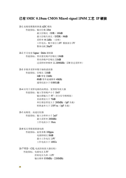
已有SMIC 0.18um CMOS Mixed-signal 1P6M工艺IP硬核18-1高精度模数转换器ADC模块性能指标:输出位数18bit最大信噪比(SNR)100dB最大信噪失真比(SNDR)96dB采样率44.1kHz (音频)工作电压:数字部分1.8V 模拟部分3V整体功耗20mW18-2开关电容Sigma-Delta调制器性能指标:带内量化噪声信噪比130dB带内热噪声信噪比110dB过采样时钟频率11.2896MHz(256倍过采样率)18-3多极多采样率数字抽取滤波器性能指标:信噪比110dB3dB带宽22kHz60dB带外衰减频率40kHz通带纹波小于0.0001dB18-4应用于采样电路的高增益、宽带跨导放大器性能指标:输入等效噪声小于10uV输出摆幅大于4V(差分信号峰峰值)直流增益大于70dB单位增益带宽大于200MHz(3pF负载)转换速率大于150V/us(3pF负载)18-5高精度、高速比较器性能指标:输入分辨率小于2mV最大采样率200MHz工作电流小于50uA18-6低压带隙基准源电路性能指标:温度系数100ppm电源抑制比80dB最小工作电压1.9V工作电流小于100Ua18-7 VCO(CSL电流控制放大器结构)性能指标:电源电压3.3V控制电压为0~1.8V输出频率850MHz~2280MHz功耗6.6mW。
相位噪声仿真值-78dBc@1MHz,测试值为-65dBc@1MHz。
18-8. VCO(差分环型振荡器结构)性能指标:电源电压1.8V控制电压为0~1.5V输出频率1.33GHz~1.93GHz功耗36mW相位噪声仿真值-107dBc@1MHz,测试值为-89dBc@1MHz。
18-9. 射频分频器性能指标:电源电压1.8V,最高工作频率2.3GHz。
18-10. 鉴频鉴相器性能指标:电源电压1.8V,无死区,操作频率仿真值500MHz。
对输入信号的占空比没有要求,引入噪声低。
高性能CMOS鉴频鉴相器和电荷泵的设计

[3]
些小的脉冲电流形成了输出信号噪声 。
信号,另一路输入信号是来自于通过分频器后的输
点:泄漏电流、电荷泵充放电电流的差异、锁定状态
信号从而修正振荡器信号和石英晶体参考信号的
下电荷泵充电脉冲和放电脉冲的不匹配。
频率和相位差。
PFD 的导通时间和延时失配是由 PFD 的结构决
定的,而电流失配和电荷泵电流大小是由电荷泵的
a phase frequency detector and charge pump circuit which is applied to atomic clock’s 3.4 GHz excitation
source is designed. The phase frequency detector consists of two edge ⁃ triggered,resettable D flipflops
里,由于脉冲电平没有到达足够开启 MOS 管的电平
要求,导致电荷泵无法正常工作,也就无法通过改变
压控振荡器的控制电压使得输入信号稳定。死区效
平,那么 S2 管导通,CP 通过 I2 放电,Vout 减小 [6-8]。如图 2
(b)所示,信号 A 频率大于信号 B,则 UP 产生连续的高
电 平 ,推 动 Vout 增 大 ,通 过 环 路 反 馈 使 得 信 号 B 频 率
2. College of Electrical Engineering,Zhejiang University of Water Resources and Electric Power,
Hangzhou 310018,China;3. School of Electical and Control Engineering,North University of China,
- 1、下载文档前请自行甄别文档内容的完整性,平台不提供额外的编辑、内容补充、找答案等附加服务。
- 2、"仅部分预览"的文档,不可在线预览部分如存在完整性等问题,可反馈申请退款(可完整预览的文档不适用该条件!)。
- 3、如文档侵犯您的权益,请联系客服反馈,我们会尽快为您处理(人工客服工作时间:9:00-18:30)。
1.
INTRODUCTION
ቤተ መጻሕፍቲ ባይዱ
With 0.18~m, we are seeing widespread use of Cu interconnect, rapid reductions in V,, and the rapid introduction of embedded modules for system-on-chip. As we move beyond the 0.18pm node, the SIA Roadmap continues to accelerate. Some proposals put the 35nm node in only 2009 (Figure I), leading to renewed examination of the limits to simple scaling rules for the transistor performance. In particular, there are serious questions on the sustainability of voltage scaling, and how the breakdown of this crucial rule will affect circuit performance. This paper will review the various impending disasters in the transistor performance, and conclude that the most serious challenges lie in the properties that have never scaled. Lithography is expected to be the gating item in the Roadmap, and in reality the availability of suitable tools will control how rapidly the minimum dimensions can be reduced. The further acceleration that has been proposed will probably be constrained by the absence of commercial lithographic processes. The most likely solution to this new challenge involves rapid deployment of enhancement technologies in optical lithography, followed by insertion of a post-optical lithography at the earliest possible point. Currently, this is likely to occur at the lOOnm and 70nm nodes, making SCALPEL much the likeliest NextGeneration Lithography.
Given the required gate dimension, traditional scaling reduces all lengthscales and voltages while increasing the doping level in order to achieve comparable fields everywhere. This has greatly simplified approach to design in successive technologies, and departure from this rule would vastly complicate the design. With an accelerating Roadmap, a breakdown in simple scaling is widely feared once the thermal limit (Vt B 0.3V) is approached. Potential solutions discussed in the literature include SoI, as well as more radical departures such as dual-gate transistors, and lowering the operating temperature. At this point there is good reason to believe that these approaches will not be economically necessary for several more technology nodes. However, design challenges continue to be dominated by circuit-level features that have never scaled appropriately. Power densities will continue to increase, and power management will become an increasingly important part of system design. Similarly, the history of interconnect management is of a long fight against the unfavourable scaling of the resistance and interconnect delay. By default, RC time-constants increase very rapidly as the L,ff scales down, a problem which is exacerbated if it is viewed in terms of clock-cycles. Traditionally, this has been tackled by adding more layers of metal. Over the next few years, most process flows will migrate to Cu metallisation, with a transition point dictated by process cost and chip dimensions. However, the ultimate solution requires explicitly handling latency at the system level.
40.1
0.18p.m CMOS and beyond
D.J. Eaglesham Bell Labs, Lucent Technologies, 600 Mountain Avenue, Murray Hill, NJ 07974
deaglesham@
ABSTRACT
As we move to the 0.18pm node and beyond, the dominant trend in device and process technology is a simple continuation of several decades of scaling. However, some serious challenges to straightforward scaling are on the horizon. This paper will review the present status of process technology and examine the likely departures from scaling in the various areas. The 0.18pm node is seeing the first major new materials introduced into the Si process for many years in the interconnect, and major departures from the traditional process are being actively considered for the transistor. However, it is probable that continued scaling will continue to dominate advanced processes for several generations to come.
Permission to make digital or hard copies of all or part of this work for personal or classroom use is granted without fee provided that copies are not made or distributed for profit or commercial advantage and that copies bear this notice and the full citation on the first page. To copy otherwise, to republish, to post on servers or to redistribute to lists, requires prior specificpermission and/or a fee. DAC 99,New Orleans, Louisiana 81999 ACM 1-58113-092-9/99/0006..$5.00
THE ACCELERATING ROADMAP