SPV1001N40;SPV1001N30;中文规格书,Datasheet资料
PN8370 Datasheet中文版 Rev.A.1511-690V
T=
C
25℃)……………………………….…..….……...………….…..………….……....….....1.5W
损耗功率
PD
(DIP-8,
T=
C
25℃)…………………………………..….….…..………..……..……………….………....3W
最大漏极直流电流
(ID
,
SOP-7,
T=
C
25℃)…………………………………………………..……………..…………0.55A
最大漏极直流电流
(ID
,
DIP-8,
T=
C
25℃)…………..……………………………………..…………….….…………0.8A
最大漏极脉冲电流
(IDP,
T=
C
25℃)…………..……………….…………………………….…...……….….…………3.0A
备注:1. 产品委托第三方严格按照芯片级 ESD 标准(ESDA/JEDEC JDS-001-2014)中的测试方式和流程进行测试。
PN8370
Chipown
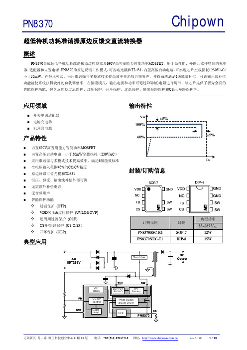
超低待机功耗准谐振原边反馈交直流转换器
概述
PN8370集成超低待机功耗准谐振原边控制器及690V高雪崩能力智能功率MOSFET,用于高性能、外围元器件精简的充电 器、适配器和内置电源。PN8370为原边反馈工作模式,可省略光耦和TL431。内置高压启动电路,可实现芯片空载损耗(230VAC) 小于30mW。在恒压模式,采用准谐振与多模式技术提高效率并消除音频噪声,使得系统满足6级能效标准,可调输出线补偿 功能能使系统获得较好的负载调整率;在恒流模式,输出电流和功率可通过CS脚的电阻进行调节。该芯片提供了极为全面的 智能保护功能,包含逐周期过流保护、过压保护、开环保护、过温保护、输出短路保护和CS开/短路保护等。
DMN601TK-7;中文规格书,Datasheet资料
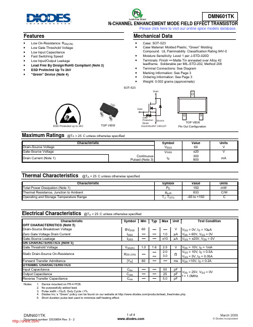
Features• Low On-Resistance: R DS(ON) • Low Gate Threshold Voltage • Low Input Capacitance • Fast Switching Speed• Low Input/Output Leakage• Lead Free By Design/RoHS Compliant (Note 2) • ESD Protected Up To 2kV • "Green" Device (Note 4)Mechanical Data• Case: SOT-523 • Case Material: Molded Plastic, “Green” MoldingCompound. UL Flammability Classification Rating 94V-0 • Moisture Sensitivity: Level 1 per J-STD-020D • Terminals: Finish ⎯ Matte Tin annealed over Alloy 42leadframe. Solderable per MIL-STD-202, Method 208 • Terminal Connections: See Diagram • Marking Information: See Page 3 • Ordering Information: See Page 3 • Weight: 0.002 grams (approximate)Maximum Ratings @T A = 25°C unless otherwise specifiedCharacteristicSymbol Value Units Drain-Source Voltage V DSS 60 VGate-Source Voltage V GSS±20 V Drain Current (Note 1) ContinuousPulsed (Note 3)I D300800mAThermal Characteristics @T A = 25°C unless otherwise specifiedCharacteristicSymbol Value Units Total Power Dissipation (Note 1)P D 150 mW Thermal Resistance, Junction to Ambient R θJA 833 °C/W Operating and Storage Temperature Range T J , T STG-65 to +150°CElectrical Characteristics @T A = 25°C unless otherwise specifiedCharacteristicSymbol Min Typ Max UnitTest ConditionOFF CHARACTERISTICS (Note 5) Drain-Source Breakdown Voltage BV DSS 60 ⎯ ⎯ V V GS = 0V, I D = 10μA Zero Gate Voltage Drain Current I DSS ⎯ ⎯ 1.0 μA V DS = 60V, V GS = 0V Gate-Source LeakageI GSS ⎯ ⎯ ±10 μA V GS = ±20V, V DS = 0V ON CHARACTERISTICS (Note 5) Gate Threshold VoltageV GS(th) 1.0 1.6 2.5 VV DS = 10V, I D = 1mA Static Drain-Source On-Resistance R DS (ON) ⎯ ⎯ ⎯ 2.0 3.0 ΩV GS = 10V, I D = 0.5A V GS = 5V, I D = 0.05A Forward Transfer Admittance |Y fs | 80 ⎯ ⎯ ms V DS =10V, I D = 0.2A DYNAMIC CHARACTERISTICS Input Capacitance C iss ⎯ ⎯ 50 pF V DS = 25V, V GS = 0V f = 1.0MHz Output CapacitanceC oss ⎯ ⎯ 25 pF Reverse Transfer CapacitanceC rss⎯⎯5.0pFNotes: 1. Device mounted on FR-4 PCB. 2. No purposefully added lead.3. Pulse width ≤10μS, Duty Cycle ≤1%4. Diodes Inc.’s “Green” policy can be found on our website at /products/lead_free/index.php.5. Short duration pulse test used to minimize self-heating effect.SOT-523TOP VIEWPin Out ConfigurationESD Protected up to 2kVEQUIVALENT CIRCUITPlease click here to visit our online spice models database.V , DRAIN-SOURCE VOLTAGE (V)Fig. 1 Typical Output CharacteristicsDS I , D R A I N C U R R E N T (A )DFig. 2 Typical Transfer CharacteristicsGS T , CHANNEL TEMPERATURE (°C)Fig. 3 Gate Threshold Voltage vs. Channel T emperaturech 00.51.5I DRAIN CURRENT (A)Fig. 4 Static Drain-Source On-Resistancevs. Drain CurrentD , R , S T A T I C D R A I N -S O U R CE D S (O N)Fig. 5 Static Drain-Source On-Resistancevs. Drain CurrentDR , S T A T I C D R A I N -S O U R C E D S (O N )V GATE SOURCE VOLTAGE (V)Fig. 6 Static Drain-Source On-Resistancevs. Gate-Source VoltageGS,R , S T A T I C D R A I N -S O U R C E O N -R E S I S T A N C E ()D S (O N )ΩFig. 7 CH Static Drain-Source On-State Resistancevs. Channel T emperatureR , S T A T I C D R A I N -S O U R C E D S (O N )1I , R E V E R S E D R A I N C U R RE N T (A )D R 1I , DRAIN CURRENT (A)D Fig.10 Forward Transfer Admittancevs. Drain CurrentOrdering Information (Note 6)Part Number Case Packaging DMN601TK-7SOT-523 3000/Tape & ReelNotes: 6. For packaging details, go to our website at /datasheets/ap02007.pdf.Marking InformationDate Code KeyYear 2005 2006 2007 2008 2009 2010 2011 2012 Code S T U V W X Y ZMonth Jan Feb Mar Apr May Jun Jul Aug Sep Oct Nov Dec Code 1 2 3 4 5 6 7 8 9 O N DK7K = Product Type Marking Code YM = Date Code Marking Y = Year (ex: S = 2005) M = Month (ex: 9 = September) K7K YMPackage Outline DimensionsSuggested Pad LayoutIMPORTANT NOTICEDiodes Incorporated and its subsidiaries reserve the right to make modifications, enhancements, improvements, corrections or other changes without further notice to any product herein. Diodes Incorporated does not assume any liability arising out of the application or use of any product described herein; neither does it convey any license under its patent rights, nor the rights of others. The user of products in such applications shall assume all risks of such use and will agree to hold Diodes Incorporated and all the companies whose products are represented on our website, harmless against all damages.LIFE SUPPORTDiodes Incorporated products are not authorized for use as critical components in life support devices or systems without the expressed written approval of the President of Diodes Incorporated.SOT-523Dim Min Max Typ A 0.15 0.30 0.22 B 0.75 0.85 0.80 C 1.45 1.75 1.60 D ⎯ ⎯ 0.50 G 0.90 1.10 1.00 H 1.50 1.70 1.60 J 0.00 0.10 0.05 K 0.60 0.80 0.75 L 0.10 0.30 0.22 M 0.10 0.20 0.12 N 0.45 0.65 0.50α0° 8° ⎯ All Dimensions in mmDimensions Value (in mm)Z1.8 X 0.4 Y 0.51 C 1.3 E 0.7X EYCZ分销商库存信息: DIODESDMN601TK-7。
SDX15D4;SDX15A2;SDX01G2;SDX100G2;SDX01D4;中文规格书,Datasheet资料

SDX SeriesPlastic Silicon Pressure SensorsLow Cost, TemperatureCompensated, DIP, 0 psi to 1 psi, 0 psi to 100 psiDESCRIPTIONThe SDX Series sensors provide a very cost-effective solution for pressure applications that require small size plusperformance. These calibrated and temperature-compensated sensors give an accurate and stable output over a 0 °C to 50 °C [32 °F to 122 °F] temperature range. This series is intended for use with non-corrosive, non-ionic working fluids such as air and dry gases.Devices are available to measure absolute and gage pressures from 1 psi (SDX01) up to 100 psi (SDX100). The absolute devices have an internal vacuum reference and an output voltage proportional to absolute pressure. The SDX devices are available in standard commercial and prime grades(SDCXXXXX -A ) to allow optimization of accuracy and cost in any given application.The SDX devices feature an integrated circuit (IC) sensor element and laser trimmed thick film ceramic housed in acompact solvent resistant case. The package is a double-wide, dual-inline package (DIP). This is the same familiar package used by IC manufacturers except it is only 11,94 mm [0.470 in] long and has a pressure port(s). The PC board area used by each DIP is approximately 0.26 in 2. This extremely small size enables the use of multiple sensors in limited available space. The DIP provides excellent corrosion resistance and isolation to external package stress.The DIP mounts on a PC board like a standard IC withthrough-hole pins. The pins anchor the pressure sensor to the PC board and provide a more secure and stable unit than other types of packages.The output of the bridge is ratiometric to the supply voltage and operation from any dc supply voltage up to 20 Vdc is acceptable.FEATURES • Low cost DIP• Precision temperature compensation • Calibrated zero and span • Small size • Low noise• High impedance for low power applications POTENTIAL APPLICATIONS • Medical equipment • Computer peripherals • Pneumatic controls • HVAC • Prime grade available (SDXxxxyy-A)SDX Series2 /sensingTable 1. Pressure Range Specifications and Ordering InformationCatalog Listing, Pressure Connection,Pressure TypeFull-Scale Span (1) Gage Differential/Gage AbsoluteOperating PressureProof Pressure (2) Min. Typ. Max. SDX01G2 SDX01D4 - 17.37 mV 18.00 mV 18.18 mVSDX01G2-A SDX01D4-A - 0 psid to 1 psid 20 psid17.82 mV 18.00 mV 18.80 mV SDX05G2 SDX05D4 - 57.90 mV 60.00 mV 62.10 mVSDX05G2-A SDX05D4-A - 0 psid to 5 psid 20 psid59.40 mV 60.00 mV 60.60 mV SDX15G2 SDX15D4 - 86.85 mV 90.00 mV 93.15 mVSDX15G2-A SDX15D4-A - 0 psid to 15 psid 30 psid89.10 mV 90.00 mV 90.90 mV- - SDX15A2 86.85 mV 90.00 mV 93.15 mV - - SDX15A4 86.85 mV 90.00 mV 93.15 mV- - SDX15A2-A 89.10 mV 90.00 mV 90.90 mV - - SDX15A4-A 0 psia to 15 psia 30 psia89.10 mV 90.00 mV 90.90 mVSDX30G2 SDX30D4 - 86.85 mV 90.00 mV 93.15 mVSDX30G2-A SDX30D4-A - 0 psid to 30 psid 60 psid89.10 mV 90.00 mV 90.90 mV- - SDX30A2 86.85 mV 90.00 mV 93.15 mV - - SDX30A4 86.85 mV 90.00 mV 93.15 mV- - SDX30A2-A 89.10 mV 90.00 mV 90.90 mV - - SDX30A4-A 0 psia to 30 psia 60 psia89.10 mV 90.00 mV 90.90 mVSDX100G2 SDX100D4 - 96.50 mV 100.00 mV 103.5 mVSDX100G2-A SDX100D4-A- 0 psid to 100 psid 150 psid99.00 mV 100.00 mV 101.0 mV - - SDX100A2 96.50 mV 100.00 mV 103.5 mV - - SDX100A4 96.50 mV 100.00 mV 103.5 mV - - SDX100A2-A 99.00 mV 100.00 mV 101.0 mV- - SDX100A4-A0 psia to 100psia 150 psia99.00 mV 100.00 mV 101.0 mV Nomenclature Pressure Connection (See Fig. 2)Pressure Type GradeG2 A2/G2 gage standard commercial G2-A A2/G2 gage prime D4 OK differential standard commercial D4-A OK differential prime A2 A2/G2 absolute standard commercial A2-A A2/G2 absolute prime A4 A4 absolute standard commercial A4-A A4 absolute primeTable 2. General Specifications (Maximum)Characteristic ParameterSupply voltage (V S) 20 Vdc Common mode pressure 150 psig Lead soldering temperature (2 s to 4 s) 250 °C [482 °F]Table 3. Environmental Specifications (Maximum)Characteristic Parameter Compensated operating temperature 0 °C to 50 °C [32 °F to 122 °F] Operating temperature -40 °C to 85 °C [-40 °F to 185 °F] Storage temperature -55 °C to 125 °C [-67 °F to 257 °F] Humidity limits 0% RH to 100% RHPlastic Silicon Pressure Sensors, Low Cost, TemperatureCompensated, DIP, 0 psi to 1 psi, 0 psi to 100 psiHoneywell Sensing and Control 3Table 4. Performance Characteristics (3)Characteristic Min. Typ. Max. Unit Zero pressure offset Zero pressure offset (prime grade) (4)-1.0 -0.3 0.0 0.0 +1.0 0.3 mVmV Combined linearity and hysteresis (5) Combined linearity and hysteresis (prime grade)(5) (13)– – ±0.2 ±0.1 ±1.0 ±0.25 % FSO% FSO Temperature effect on span, 0 °C to 50 °C [32 °F to 122 °F] (6)Temperature effect on span, 0 °C to 50 °C [32 °F to 122 °F] (6)(prime grade) – – ±0.4 ±0.4 ±2.0 ±1.0 % FSO% FSOTemperature effect on offset 0, °C to 50 °C [32 °F to 122 °F] (6)Temperature effect on offset 0, °C to 50 °C [32 °F to 122 °F] (6) (prime grade)– – ±0.2 ±0.2 ±1.0 ±0.5 mVmV Repeatability (7)– ±0.2 ±0.5 % FSOInput resistance (8)– 4.0 – kOhmOutput resistance (9)– 4.0 – kOhmCommon mode voltage (10)1.5 3.0 5.0 VdcResponse time (11)– 100 – µsLong term stability of offset and span (12)– ±0.1 – mV Notes:1. Full-Scale Span is the algebraic difference between the output voltage at full-scale pressure and the output at zero pressure.Full-Scale Span is ratiometric to the supply voltage.2. Maximum pressure above which causes permanent sensor failure.3. Reference conditions:• T A = 25 °C (unless otherwise noted).• Supply V S = 12 Vdc, Common Mode Line pressure = 0 psig.• Pressure applied toPort B. For absolute devices only, pressure is applied to Port A and the output polarity is reversed. 4. Maximum zero pressure offset for absolute devices is ±500 mV.5. Hysteresis is the maximum output difference at any point within the operating pressure range for increasing and decreasingpressure.6. Maximum error band of the offset voltage and the error band of the span, relative to the 25 °C [77 °F] reading.7. Maximum difference in output at any pressure within the operating pressure range and the temperature within 0 °C to 50 °C[32 °F to 122 °F] after:• 100 temperature cycles, 0 °C to 50 °C [32 °F to 122 °F]. • 1.0 million pressure cycles, 0 psi to full-scale span.8. Input resistance is the resistance between V S and ground.9. Output resistance is the resistance between the + and - outputs. 10. Common Mode voltage of the output arms for V S =12 Vdc.11. Response time for a 0 psi to Full-Scale Span pressure step change, 10% to 90% rise time. 12. Long term stability over a one-year period.13. Maximum combined linearity and hysteresis for the SDX05 prime grade is ±0.5%.Figure 1. Electrical ConnectionsFigure 2. Mounting Dimensions (For Reference Only. mm/[in])A2/G2 PackageA4 PackageD4 PackageWARNING PERSONAL INJURYDO NOT USE these products as safety or emergency stop devices or in any other application where failure of the product could result in personal injury.Failure to comply with these instructions could result in death or serious injury.WARNINGMISUSE OF DOCUMENTATION• The information presented in this product sheet is forreference only. Do not use this document as a product installation guide.• Complete installation, operation, and maintenanceinformation is provided in the instructions supplied with each product.Failure to comply with these instructions could result in death or serious injury.WARRANTY/REMEDYHoneywell warrants goods of its manufacture as being free of defective materials and faulty workmanship. Honeywell’sstandard product warranty applies unless agreed to otherwise by Honeywell in writing; please refer to your orderacknowledgement or consult your local sales office for specific warranty details. If warranted goods are returned to Honeywell during the period of coverage, Honeywell will repair or replace, at its option, without charge those items it finds defective. The foregoing is buyer’s sole remedy and is in lieu of all other warranties, expressed or implied, including those ofmerchantability and fitness for a particular purpose. In no event shall Honeywell be liable for consequential, special, or indirect damages.SALES AND SERVICEHoneywell serves its customers through a worldwide network of sales offices, representatives and distributors. Forapplication assistance, current specifications, pricing or name of the nearest Authorized Distributor, contact your local sales office or:E-mail: info.sc@Internet: /sensingPhone and Fax:While we provide application assistance personally, through our literature and the Honeywell web site, it is up to the customer to determine the suitability of the product in the application. Asia Pacific +65 6355-2828; +65 6445-3033 Fax Europe +44 (0) 1698 481481; +44 (0) 1698 481676 Fax Latin America +1-305-805-8188; +1-305-883-8257 Fax USA/Canada +1-800-537-6945; +1-815-235-6847+1-815-235-6545 FaxSpecifications may change without notice. The information we supply is believed to be accurate and reliable as of this printing. However, we assume no responsibility for its use.Sensing and Control Honeywell1985 Douglas Drive North Golden Valley, Minnesota 55422 /sensing 008103-3-EN IL50 GLO Printed in USA November 2008Copyright © 2008 Honeywell International Inc. All rights reserved.分销商库存信息:HONEYWELLSDX15D4SDX15A2SDX01G2 SDX100G2SDX01D4SDX05D4 SDX100A4SDX30D4SDX100D4 SDX30G2SDX15A4-A SDX15D4-A SDX15G2SDX30A2SDX15A4 SDX05G2SDX100A2SDX30A4 SDX15G2-A SDX15A2-A SDX100G2-A SDX01G2-A SDX05G2-A SDX05D4-A。
RIGOL QGB10000-1110 电源线保证和声明说明书

保证和声明版权©2018苏州普源精电科技有限公司商标信息RIGOL是苏州普源精电科技有限公司的注册商标。
文档编号QGB10000-1110声明●本公司产品受中国及其它国家和地区的专利(包括已取得的和正在申请的专利)保护。
●本公司保留改变规格及价格的权利。
●本手册提供的信息取代以往出版的所有资料。
●本手册提供的信息如有变更,恕不另行通知。
●对于本手册可能包含的错误,或因手册所提供的信息及演绎的功能以及因使用本手册而导致的任何偶然或继发的损失,RIGOL概不负责。
●未经RIGOL事先书面许可,不得影印、复制或改编本手册的任何部分。
产品认证RIGOL认证本产品符合中国国家产品标准和行业产品标准及ISO9001:2015标准和ISO14001:2015标准,并进一步认证本产品符合其它国际标准组织成员的相关标准。
联系我们如您在使用此产品或本手册的过程中有任何问题或需求,可与RIGOL联系:电子邮箱:*****************网址:一般安全概要1.请使用所在国家认可的本产品专用电源线。
2.请确保产品可靠接地。
3.查看所有终端额定值。
4.请使用合适的过压保护。
5.请勿开盖操作。
6.请勿将异物插入排风口。
7.请使用合适的保险丝。
8.避免电路外露。
9.怀疑产品出故障时,请勿进行操作。
10.请保持适当的通风。
11.请勿在潮湿环境下操作。
12.请勿在易燃易爆的环境下操作。
13.请保持产品表面的清洁和干燥。
14.请注意防静电保护。
15.请注意搬运安全。
16.请正确使用前面板BNC输出连接器,仅允许信号输出。
安全术语和符号本手册中的安全术语:警告警告性声明指出可能会造成人身伤害或危及生命安全的情况或操作。
注意注意性声明指出可能导致本产品损坏或数据丢失的情况或操作。
产品上的安全术语:DANGER表示您如果不进行此操作,可能会立即对您造成危害。
WARNING表示您如果不进行此操作,可能会对您造成潜在的危害。
BD139-10;BD136-16;BD139-16;BD140;BD139;中文规格书,Datasheet资料

May 2008Rev 51/9BD135 - BD136BD139 - BD140Complementary low voltage transistorFeatures■Products are pre-selected in DC current gainApplication■General purposeDescriptionThese epitaxial planar transistors are mounted in the SOT -32 plastic package. They are designed for audio amplifiers and drivers utilizingcomplementary or quasi-complementary circuits. The NPN types are the BD135 and BD139, and the complementary PNP types are the BD136 and BD140.Table 1.Device summaryOrder codes Marking Package PackagingBD135BD135SOT -32TubeBD135-16BD135-16BD136BD136BD136-16BD136-16BD139BD139BD139-10BD139-10BD139-16BD139-16BD140BD140BD140-10BD140-10BD140-16BD140-16Contents BD135 - BD136 - BD139 - BD140Contents1Electrical ratings . . . . . . . . . . . . . . . . . . . . . . . . . . . . . . . . . . . . . . . . . . . . 32Electrical characteristics . . . . . . . . . . . . . . . . . . . . . . . . . . . . . . . . . . . . . 42.1Electrical characteristics (curves) . . . . . . . . . . . . . . . . . . . . . . . . . . . . . . . 5 3Package mechanical data . . . . . . . . . . . . . . . . . . . . . . . . . . . . . . . . . . . . . 6 4Revision history . . . . . . . . . . . . . . . . . . . . . . . . . . . . . . . . . . . . . . . . . . . . 82/9BD135 - BD136 - BD139 - BD140Electrical ratings3/91 Electrical ratingsTable 2.Absolute maximum ratingsSymbolParameterValueUnitNPNPNPBD135BD139BD136BD140V CBO Collector-base voltage (I E = 0)4580-45-80V V CEO Collector-emitter voltage (I B = 0)4580-45-80V V EBO Emitter-base voltage (I C = 0)5-5V I C Collector current 1.5-1.5A I CM Collector peak current 3-3A I B Base current0.5-0.5A P TOT Total dissipation at T c ≤ 25 °C 12.5W P TOT Total dissipation at T amb ≤ 25 °C 1.25W T stg Storage temperature-65 to 150°C T jMax. operating junction temperature150°CTable 3.Thermal dataSymbolParameterMax valueUnit R thj-case Thermal resistance junction-case 10°C/W R thj-amb Thermal resistance junction-ambient100°C/WElectrical characteristics BD135 - BD136 - BD139 - BD1404/92 Electrical characteristics(T case = 25 °C unless otherwise specified)Table 4.On/off statesSymbolParameterPolarityTest conditionsValueUnitMin.Typ.Max.I CBOCollector cut-off current (I E =0)NPN V CB = 30 VV CB = 30 V , T C = 125 °C 0.110µA µA PNP V CB = -30 VV CB = -30 V , T C = 125 °C -0.1-10µA µA I EBOEmitter cut-off current (I C =0)NPN V EB = 5 V 10µA PNP V EB = -5 V -10µA V CEO(sus)(1)1.Pulsed: pulse duration = 300 µs, duty cycle 1.5%Collector-emittersustaining voltage(I B =0)NPNI C = 30 mA BD135BD1394580V V PNP I C = -30 mA BD136BD140-45-80V V V CE(sat) (1)Collector-emitter saturation voltage NPN I C = 0.5 A, I B = 0.05 A 0.5V PNP I C = -0.5 A, I B = -0.05 A -0.5V V BE (1)Base-emitter voltageNPN I C = 0.5 A, V CE = 2 V 1V PNP I C = -0.5 A, V CE = -2 V -1V h FE (1)DC current gainNPNI C = 5 mA, V CE = 2 V I C = 150 mA, V CE = 2 V I C = 0.5 A, V CE = 2 V 254025250PNPI C = -5 mA, V CE = -2 V I C = -150 mA, V CE = -2 V I C = -0.5 A, V CE = -2 V 254025250h FE (1)h FE groupsNPNI C = 150 mA, V CE = 2 V BD139-10BD135-16/BD139-1663100160250PNPI C = -150 mA, V CE = -2 V BD140-10BD136-16/BD140-1663100160250BD135 - BD136 - BD139 - BD140Electrical characteristics 2.1 Electrical characteristics (curves)Figure 2.Safe operating area Figure 3.Derating5/9Package mechanical data BD135 - BD136 - BD139 - BD140 3 Package mechanical dataIn order to meet environmental requirements, ST offers these devices in ECOPACK®packages. These packages have a lead-free second level interconnect. The category ofsecond level interconnect is marked on the package and on the inner box label, incompliance with JEDEC Standard JESD97. The maximum ratings related to solderingconditions are also marked on the inner box label. ECOPACK is an ST trademark.ECOPACK specifications are available at: 6/9BD135 - BD136 - BD139 - BD140Package mechanical data7/9Revision history BD135 - BD136 - BD139 - BD1408/94 Revision historyTable 5.Document revision historyDate RevisionChanges16-Sep-2001422-May-20085Mechanical data has been updated.BD135 - BD136 - BD139 - BD140Please Read Carefully:Information in this document is provided solely in connection with ST products. STMicroelectronics NV and its subsidiaries (“ST”) reserve the right to make changes, corrections, modifications or improvements, to this document, and the products and services described herein at any time, without notice.All ST products are sold pursuant to ST’s terms and conditions of sale.Purchasers are solely responsible for the choice, selection and use of the ST products and services described herein, and ST assumes no liability whatsoever relating to the choice, selection or use of the ST products and services described herein.No license, express or implied, by estoppel or otherwise, to any intellectual property rights is granted under this document. If any part of this document refers to any third party products or services it shall not be deemed a license grant by ST for the use of such third party products or services, or any intellectual property contained therein or considered as a warranty covering the use in any manner whatsoever of such third party products or services or any intellectual property contained therein.UNLESS OTHERWISE SET FORTH IN ST’S TERM S AND CONDITIONS OF SALE ST DISCLAIM S ANY EXPRESS OR IM PLIED WARRANTY WITH RESPECT TO THE USE AND/OR SALE OF ST PRODUCTS INCLUDING WITHOUT LIM ITATION IM PLIED WARRANTIES OF MERCHANTABILITY, FITNESS FOR A PARTICULAR PURPOSE (AND THEIR EQUIVALENTS UNDER THE LAWS OF ANY JURISDICTION), OR INFRINGEMENT OF ANY PATENT, COPYRIGHT OR OTHER INTELLECTUAL PROPERTY RIGHT. UNLESS EXPRESSLY APPROVED IN WRITING BY AN AUTHORIZED ST REPRESENTATIVE, ST PRODUCTS ARE NOT RECOMMENDED, AUTHORIZED OR WARRANTED FOR USE IN MILITARY, AIR CRAFT, SPACE, LIFE SAVING, OR LIFE SUSTAINING APPLICATIONS, NOR IN PRODUCTS OR SYSTEMS WHERE FAILURE OR MALFUNCTION MAY RESULT IN PERSONAL INJURY, DEATH, OR SEVERE PROPERTY OR ENVIRONMENTAL DAMAGE. ST PRODUCTS WHICH ARE NOT SPECIFIED AS "AUTOMOTIVE GRADE" MAY ONLY BE USED IN AUTOMOTIVE APPLICATIONS AT USER’S OWN RISK.Resale of ST products with provisions different from the statements and/or technical features set forth in this document shall immediately void any warranty granted by ST for the ST product or service described herein and shall not create or extend in any manner whatsoever, any liability of ST.ST and the ST logo are trademarks or registered trademarks of ST in various countries.Information in this document supersedes and replaces all information previously supplied.The ST logo is a registered trademark of STMicroelectronics. All other names are the property of their respective owners.© 2008 STMicroelectronics - All rights reservedSTMicroelectronics group of companiesAustralia - Belgium - Brazil - Canada - China - Czech Republic - Finland - France - Germany - Hong Kong - India - Israel - Italy - Japan - Malaysia - Malta - Morocco - Singapore - Spain - Sweden - Switzerland - United Kingdom - United States of America9/9分销商库存信息:STMBD139-10BD136-16BD139-16 BD140BD139BD135-16 BD135。
RSS100N03中文资料
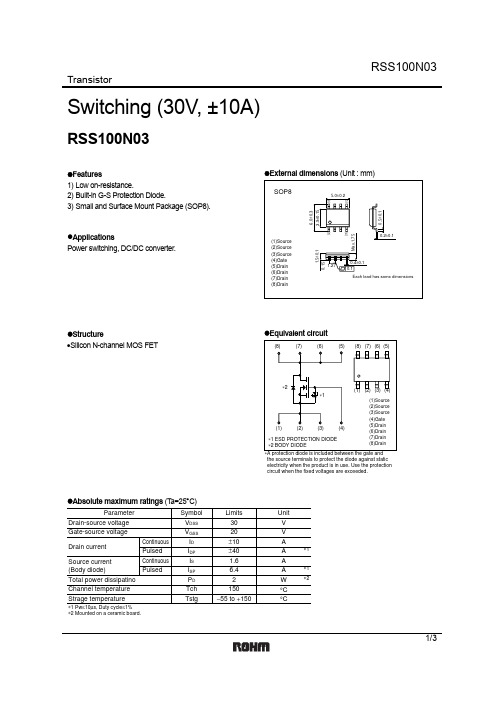
Transistor1/3Switching (30V, ±10A)RSS100N03z Features1) Low on-resistance.2) Built-in G-S Protection Diode.3) Small and Surface Mount Package (SOP8).z ApplicationsPower switching, DC/DC converter.z External dimensions (Unit : mm)z Structure•Silicon N-channel MOS FET z Equivalent circuitthe source terminals to protect the diode against static electricity when the product is in use. Use the protection circuit when the fixed voltages are exceeded.z Absolute maximum ratings (T a=25°C)∗1∗1∗2ParameterV V DSS Symbol 30V V GSS 20A I D ±10A I DP ±40A I S 1.6A I SP 6.4W P D 2°C Tch 150°CTstg −55 to +150Limits Unit Drain-source voltage Gate-source voltage Drain current Total power dissipatino Channel temperature Strage temperatureContinuous Pulsed Continuous Source current (Body diode)Pulsed∗1 Pw ≤10µs, Duty cycle ≤1%∗2 Mounted on a ceramic board.Transistor2/3z Thermal resistance (T a=25°C)°C / WRth (ch-a)62.5ParameterSymbol Limits Unit Channel to ambient∗ Mounted on a ceramic board.∗z Electrical characteristics (T a=25°C)z Body diode characteristics (Source-Drain Characteristics) (T a=25°C)Forward voltageV SD −− 1.2V I S=6.4A, V GS =0VParameterSymbol Min.Typ.Max.Unit Conditions∗Pulsed∗z Electrical characteristic curvesDRAIN-SOURCE VOLTAGE : V DS (V)C A P A C I T A N C E : C (p F )Fig.1 Typical Capacitancevs. Drain-Source VoltageDRAIN CURRENT : I D (A)S W I T C H I N G T I M E : t (n s )Fig.2 Switching CharacteristicsTOTAL GATE CHARGE : Qg (nC)G A T E -S O U R C E V O L T A G E : V G S (V )Fig.3 Dynamic Input CharacteristicsTransistor3/3GATE-SOURCE VOLTAGE : V GS (V)D R A I N C U R RE N T : I D (A )Fig.4 Typical Transfer CharacteristicsGATE-SOURCE VOLTAGE : V GS (V)S T A T I C D R A I N -S O U R C E O N -S T A T E R E S I S T A N C E : R D S (o n ) (m Ω)Fig.5 Static Drain-SourceOn-State Resistance vs. Gate-Source VoltageSOURCE-DRAIN VOLTAGE : V SD (V)S O U R C E C U R R E N T : I s (A )Fig.6 Source Current vs.Source-Drain VoltageDRAIN CURRENT : I D (A)1101001000S T A T I C D R A I N -S O U R C E O N -S T A T E R E S I S TA N C E : R D S (o n ) (m Ω)Fig.7 Static Drain-SourceOn-State Resistance vs. Drain Current (Ι)DRAIN CURRENT : I D (A)S T A T I C D R A I N -S O U R C E O N -S T A T E R E S I S T A N C E : R D S (o n ) (m Ω)Fig.8 Static Drain-SourceOn-State Resistance vs. Drain Current (ΙΙ)DRAIN CURRENT : I D (A)S T A T I C D R A I N -S O U R C E O N -S T A T E R E S I S T A N C E : R D S (o n ) (m Ω)Fig.9 Static Drain-SourceOn-State Resistance vs. Drain Current (ΙΙΙ)AppendixAbout Export Control Order in JapanProducts described herein are the objects of controlled goods in Annex 1 (Item 16) of Export Trade ControlOrder in Japan.In case of export from Japan, please confirm if it applies to "objective" criteria or an "informed" (by MITI clause)on the basis of "catch all controls for Non-Proliferation of Weapons of Mass Destruction.Appendix1-Rev1.0。
TP1001中文资料_TP1001规格书_TP1001 PDF

QC2.0 协议接口
TP1001 启动时,当 VDD 电压达到芯片启动电压阈值后 的 20ms 或更短时间内,开关 N5 导通(见内部框图)。此 时开关 N4 以及输出控制开关 N1~N3 保持关断。这时电 源设定为默认的 5 V 输出电压值。当 D+和 D-短路后,就 可以开始 USB 电池充电规范 1.2 版本中所述的专用充电 接口(DCP)与受电设备(PD)之间的正常握手。开关 N5 导 通后,TP1001 开始监测 D+的电压值。如果该值连续高 4
特点
支持 QC2.0 协议的整个输出电压范围 A 类规范:5V,9V 和 12V B 类规范:5V,9V,12V 和 20V 兼容 USB 电池充电规范 1.2 版本 自动 USB DCP 短路 D+至 D默认 5V 输出模式 芯片超低工作电流,待机功耗低 5V 输出电压时功耗低于 1mW 5~20V 的宽芯片供电电压 可选的 B 类规范输出电压抑制功能 芯片引脚开路保护功能 芯片相邻引脚短路保护功能 芯片供电欠压保护 系统 BOM 成本低 采用 SOP8L 封装
保护功能
TP1001 具有多种保护功能以保证系统的稳定和可靠。 包 括可选的 B 类规范输出电压抑制,芯片引脚开路保护, 芯片相邻引脚短路保护和芯片供电欠压保护等。 当 TP1001 只应用在 QC2.0 协议的 A 类规范的输出电压 范围(5V,9V,12V)时,可以通过将芯片的 V3 引脚短接到 VDD 来实现。此时 TP1001 抑制受电设备通过数据线路 D+和 D-施加的任何 20V 输出电压的请求。
Shenzhen TPOWER Semiconductor
TP1001 支持 QC2.0 快速充电协议的接口控制芯片
ISO1001隔离放大器模块及应用精品资料

ISO 1001 隔离放大器模块及应用连续隔离电压值: 3000VDC 电源电压输入范围: ±15%Vin 焊接温度(10秒): +300℃ 输出最小负载: 2K Ω图2 典型接线图图7 输出放大器调节电路图6 输出放大器原理图例如:当输入Vin 为0~+100mV ,输出为0~5V 时,可以取:R11=51K R12=10K R13=10K 放大倍数Kin=1+39.9/10=4.99在图4和图5中,R11也可以由一个电位器和一个电阻串联来代替,可以精确调节放大倍。
产品图片及引脚定义(图10、图11)图10 产品图片 图11 引脚定义建议印刷布板尺寸(标准DIP24脚) 引脚功能描述外形尺寸Pin 引脚Connection 功能描述 1 输出VS1 输入端可用负电源 2 输出GND1 VS1和VD1电源地 3 输出VD1 输入端可用正电源 4~5 NC 空脚Omitted 6 输入VD 输入辅助电源 7 输入GND 输入辅助电源地 8~9 NC 空脚Omitted 10 输出VS2 输出端可用负电源 11 输出GND2 VS2和VD2电源地12 输出VD2 输出端可用负电源 13 输出VOUT 隔离后运放输出端 14 输入FB 隔离后运放反馈端15 输入ADJ 调零输入端 16输出VREF2 输出端可用+5V 基准电源17 NC 空脚Omitted 18 NC 空脚Omitted 19 NC 空脚Omitted 20 NC 空脚Omitted 21 输出COM 输入放大器输出端 22 输入IN+ 输入正端 23 输入IN- 输入负端 24 输出VREF1 输入端可用+5V 基准电源和输入放大器组成一个数据放大器 则数据放大器的放 (多圈电位器)。
- 1、下载文档前请自行甄别文档内容的完整性,平台不提供额外的编辑、内容补充、找答案等附加服务。
- 2、"仅部分预览"的文档,不可在线预览部分如存在完整性等问题,可反馈申请退款(可完整预览的文档不适用该条件!)。
- 3、如文档侵犯您的权益,请联系客服反馈,我们会尽快为您处理(人工客服工作时间:9:00-18:30)。
November 2011Doc ID 018938 Rev 21/9SPV1001NCool bypass switch for photovoltaic applicationsFeatures■SPV1001N30 I F =12.5 A, V R =30 V ■SPV1001N40 I F =12.5 A, V R =40 V ■Very low forward voltage drop ■Very low reverse leakage current ■150 °C operating junction temperatureApplications■Photovoltaic panelsDescriptionThe SPV1001N is a system-in-package solution for photovoltaic applications to perform cool bypass rectification similar to that of aconventional Schottky diode but with much lower forward voltage drop and reverse leakage current.The device consists of a power MOSFETtransistor which charges a capacitor during the OFF time, and drives its gate during the ON time using the charge previously stored in the capacitor.The ON and OFF times are set to reduce the average voltage drop across the drain and source terminals, resulting in reduced power dissipation.PQFN 5 x 6 mmAnodoCatodoTable 1.Device summaryOrder codes Package Packaging SPV1001N30PQFN 5 x 6 mmTape and reelSPV1001N40Maximum ratings SPV1001N2/9Doc ID 018938 Rev 21 M aximum ratings1.1Absolute maximum ratings1.2 Thermal dataTable 2.Absolute maximum ratingsSymbol ParameterValueUnitSPV1001N30SPV1001N40V RMax DC reverse voltage3040V I F Max forward current 12.512.5 A I FSMNon repetitive peak surge (half-wave, singlephase 50-60 Hz)250250A ESD level Human body level ≥8 k ≥8 kV Table 3.Thermal dataSymbol ParameterValue Unit T J Junction temperature operating range -40 to 150 -40 to 150°C T STGStorage temperature range-40 to 150-40 to 150°C R thJC Thermal resistance, junction-to-case44°C/WSPV1001N Electrical characteristicsDoc ID 018938 Rev 23/92 Electrical characteristicsNote:For correct power dissipation and heatsink sizing, please refer to Figure 1, 2 e 4Table 4.Electrical characteristicsSymbolParameterTest conditionsSPV1001 N30SPV1001 N40UnitMin.Typ.Max.Min.Typ.Max.V F ,AVGAVG forward voltage dropIF = 10AT J = 25°C -120--140-mV IF = 5AT J = 25°C -70--85-mV T J = 125°C -240--280-mV I RReverse leakage current VR = 30VT J = 25°C -1--1-µA T J = 125°C -10--10-µA D TON/T ratio IF = 5AT J = 25°C -95%--95%--T J = 125°C -75%--75%--V FForward voltage dropIF = 5A, T OFFT J = 25°C -850--850-mV T J = 125°C -600--600-mV IF = 5A, T ONT J = 25°C -35--40-mV T J = 125°C-135--160-mVDevice description SPV1001N4/9Doc ID 018938 Rev 23 Device descriptionA photovoltaic panel consists of a series of PV cells. In optimal conditions, all the cells areequally irradiated and function at the same current level. However, during normal operation some cells may become partially shaded or obscured. These shaded cells limit the current generated by the fully irradiated cells and, in the extreme cases where these cells are totally obscured, the current flow is blocked.In this case the shaded cells behave like a load, and the current generated from the fully irradiated cells produces overvoltages which can reach the breakdown threshold. This phenomenon, known as a “hot spot”, can cause overheating of the shaded cells and, in some cases, even permanent damage resulting in current leakage. To prevent hot spots, therefore, bypass diodes are connected in parallel to the cell strings.The device described here has the same functionality as a Schottky diode, but with improved performance. It features very low forward voltage drop and reverse leakagecurrent. It consists of a power MOSFET transistor which charges a capacitor during the OFF time, and drives its gate during the ON time using the charge previously stored in the capacitor. The ON and OFF times are set to reduce the average voltage drop across the drain and source terminals, resulting in reduced power dissipation.SPV1001NDevice descriptionDoc ID 018938 Rev 25/9Figure 1.Average forward power dissipation vs average forward current @ 25°CFigure 2.Average forward power dissipation vs average forward current @ 75°C Figure 3.Reverse current Figure 4.Thermal resistance junction-to-ambient vs copper surface under(1)1.Epoxy printed board FR4, Cu = 35 µmPackage mechanical data SPV1001N 4 Package mechanical dataIn order to meet environmental requirements, ST offers these devices in different grades ofECOPACK® packages, depending on their level of environmental compliance. ECOPACK®specifications, grade definitions and product status are available at: .ECOPACK® is an ST trademark.Table 5.PQFN 5 x 6 mm mechanical datammDim.Min.Typ.Max.A0.850.800.95A10.0200.05D 5.00D2 4.26 4.16 4.36E 6.00E2 2.50 2.40 2.60e 1.27L 1.20 1.10 1.30L10.30NXb0.456/9Doc ID 018938 Rev 2SPV1001N Package mechanical dataDoc ID 018938 Rev 27/9Revision history SPV1001N8/9Doc ID 018938 Rev 25 Revision historyTable 6.Document revision historyDate RevisionChanges20-Jun-20111Initial release 16-Nov-20112Updated Figure 3SPV1001NPlease Read Carefully:Information in this document is provided solely in connection with ST products. STMicroelectronics NV and its subsidiaries (“ST”) reserve the right to make changes, corrections, modifications or improvements, to this document, and the products and services described herein at any time, without notice.All ST products are sold pursuant to ST’s terms and conditions of sale.Purchasers are solely responsible for the choice, selection and use of the ST products and services described herein, and ST assumes no liability whatsoever relating to the choice, selection or use of the ST products and services described herein.No license, express or implied, by estoppel or otherwise, to any intellectual property rights is granted under this document. If any part of this document refers to any third party products or services it shall not be deemed a license grant by ST for the use of such third party products or services, or any intellectual property contained therein or considered as a warranty covering the use in any manner whatsoever of such third party products or services or any intellectual property contained therein.UNLESS OTHERWISE SET FORTH IN ST’S TERM S AND CONDITIONS OF SALE ST DISCLAIM S ANY EXPRESS OR IM PLIED WARRANTY WITH RESPECT TO THE USE AND/OR SALE OF ST PRODUCTS INCLUDING WITHOUT LIM ITATION IM PLIED WARRANTIES OF MERCHANTABILITY, FITNESS FOR A PARTICULAR PURPOSE (AND THEIR EQUIVALENTS UNDER THE LAWS OF ANY JURISDICTION), OR INFRINGEMENT OF ANY PATENT, COPYRIGHT OR OTHER INTELLECTUAL PROPERTY RIGHT. UNLESS EXPRESSLY APPROVED IN WRITING BY TWO AUTHORIZED ST REPRESENTATIVES, ST PRODUCTS ARE NOT RECOMMENDED, AUTHORIZED OR WARRANTED FOR USE IN MILITARY, AIR CRAFT, SPACE, LIFE SAVING, OR LIFE SUSTAINING APPLICATIONS, NOR IN PRODUCTS OR SYSTEMS WHERE FAILURE OR MALFUNCTION MAY RESULT IN PERSONAL INJURY, DEATH, OR SEVERE PROPERTY OR ENVIRONMENTAL DAMAGE. ST PRODUCTS WHICH ARE NOT SPECIFIED AS "AUTOMOTIVE GRADE" MAY ONLY BE USED IN AUTOMOTIVE APPLICATIONS AT USER’S OWN RISK.Resale of ST products with provisions different from the statements and/or technical features set forth in this document shall immediately void any warranty granted by ST for the ST product or service described herein and shall not create or extend in any manner whatsoever, any liability of ST.ST and the ST logo are trademarks or registered trademarks of ST in various countries.Information in this document supersedes and replaces all information previously supplied.The ST logo is a registered trademark of STMicroelectronics. All other names are the property of their respective owners.© 2011 STMicroelectronics - All rights reservedSTMicroelectronics group of companiesAustralia - Belgium - Brazil - Canada - China - Czech Republic - Finland - France - Germany - Hong Kong - India - Israel - Italy - Japan - Malaysia - Malta - Morocco - Philippines - Singapore - Spain - Sweden - Switzerland - United Kingdom - United States of AmericaDoc ID 018938 Rev 29/9分销商库存信息:STMSPV1001N40SPV1001N30。