54FCT541中文资料
SN54AHCT541中文资料

PACKAGING INFORMATIONOrderable Device Status(1)PackageType PackageDrawingPins PackageQtyEco Plan(2)Lead/Ball Finish MSL Peak Temp(3)5962-9685801Q2A ACTIVE LCCC FK201TBD Call TI Level-NC-NC-NC 5962-9685801QRA ACTIVE CDIP J201TBD Call TI Level-NC-NC-NC 5962-9685801QSA ACTIVE CFP W201TBD Call TI Level-NC-NC-NC SN74AHCT541DBLE OBSOLETE SSOP DB20TBD Call TI Call TISN74AHCT541DBR ACTIVE SSOP DB202000Green(RoHS&no Sb/Br)CU NIPDAU Level-1-260C-UNLIMSN74AHCT541DBRE4ACTIVE SSOP DB202000Green(RoHS&no Sb/Br)CU NIPDAU Level-1-260C-UNLIMSN74AHCT541DW ACTIVE SOIC DW2025Green(RoHS&no Sb/Br)CU NIPDAU Level-1-260C-UNLIMSN74AHCT541DWE4ACTIVE SOIC DW2025Green(RoHS&no Sb/Br)CU NIPDAU Level-1-260C-UNLIMSN74AHCT541DWR ACTIVE SOIC DW202000Green(RoHS&no Sb/Br)CU NIPDAU Level-1-260C-UNLIMSN74AHCT541DWRE4ACTIVE SOIC DW202000Green(RoHS&no Sb/Br)CU NIPDAU Level-1-260C-UNLIMSN74AHCT541N ACTIVE PDIP N2020Pb-Free(RoHS)CU NIPDAU Level-NC-NC-NCSN74AHCT541NE4ACTIVE PDIP N2020Pb-Free(RoHS)CU NIPDAU Level-NC-NC-NCSN74AHCT541NSR ACTIVE SO NS202000Green(RoHS&no Sb/Br)CU NIPDAU Level-1-260C-UNLIMSN74AHCT541NSRE4ACTIVE SO NS202000Green(RoHS&no Sb/Br)CU NIPDAU Level-1-260C-UNLIMSN74AHCT541PW ACTIVE TSSOP PW2070Green(RoHS&no Sb/Br)CU NIPDAU Level-1-260C-UNLIMSN74AHCT541PWE4ACTIVE TSSOP PW2070Green(RoHS&no Sb/Br)CU NIPDAU Level-1-260C-UNLIM SN74AHCT541PWLE OBSOLETE TSSOP PW20TBD Call TI Call TISN74AHCT541PWR ACTIVE TSSOP PW202000Green(RoHS&no Sb/Br)CU NIPDAU Level-1-260C-UNLIMSN74AHCT541PWRE4ACTIVE TSSOP PW202000Green(RoHS&no Sb/Br)CU NIPDAU Level-1-260C-UNLIMSN74AHCT541PWRG4ACTIVE TSSOP PW202000Green(RoHS&no Sb/Br)CU NIPDAU Level-1-260C-UNLIM SNJ54AHCT541FK ACTIVE LCCC FK201TBD Call TI Level-NC-NC-NC SNJ54AHCT541J ACTIVE CDIP J201TBD Call TI Level-NC-NC-NC SNJ54AHCT541W ACTIVE CFP W201TBD Call TI Level-NC-NC-NC (1)The marketing status values are defined as follows:ACTIVE:Product device recommended for new designs.LIFEBUY:TI has announced that the device will be discontinued,and a lifetime-buy period is in effect.NRND:Not recommended for new designs.Device is in production to support existing customers,but TI does not recommend using this part in a new design.PREVIEW:Device has been announced but is not in production.Samples may or may not be available.OBSOLETE:TI has discontinued the production of the device.(2)Eco Plan-The planned eco-friendly classification:Pb-Free(RoHS)or Green(RoHS&no Sb/Br)-please check /productcontent for the latest availability information and additional product content details.TBD:The Pb-Free/Green conversion plan has not been defined.Pb-Free(RoHS):TI's terms"Lead-Free"or"Pb-Free"mean semiconductor products that are compatible with the current RoHS requirements for all6substances,including the requirement that lead not exceed0.1%by weight in homogeneous materials.Where designed to be soldered at high temperatures,TI Pb-Free products are suitable for use in specified lead-free processes.Green(RoHS&no Sb/Br):TI defines"Green"to mean Pb-Free(RoHS compatible),and free of Bromine(Br)and Antimony(Sb)based flame retardants(Br or Sb do not exceed0.1%by weight in homogeneous material)(3)MSL,Peak Temp.--The Moisture Sensitivity Level rating according to the JEDEC industry standard classifications,and peak solder temperature.Important Information and Disclaimer:The information provided on this page represents TI's knowledge and belief as of the date that it is provided.TI bases its knowledge and belief on information provided by third parties,and makes no representation or warranty as to the accuracy of such information.Efforts are underway to better integrate information from third parties.TI has taken and continues to take reasonable steps to provide representative and accurate information but may not have conducted destructive testing or chemical analysis on incoming materials and chemicals.TI and TI suppliers consider certain information to be proprietary,and thus CAS numbers and other limited information may not be available for release.In no event shall TI's liability arising out of such information exceed the total purchase price of the TI part(s)at issue in this document sold by TI to Customer on an annual basis.元器件交易网IMPORTANT NOTICETexas Instruments Incorporated and its subsidiaries (TI) reserve the right to make corrections, modifications,enhancements, improvements, and other changes to its products and services at any time and to discontinueany product or service without notice. Customers should obtain the latest relevant information before placingorders and should verify that such information is current and complete. All products are sold subject to TI’s termsand conditions of sale supplied at the time of order acknowledgment.TI warrants performance of its hardware products to the specifications applicable at the time of sale inaccordance with TI’s standard warranty. T esting and other quality control techniques are used to the extent TIdeems necessary to support this warranty. Except where mandated by government requirements, testing of allparameters of each product is not necessarily performed.TI assumes no liability for applications assistance or customer product design. Customers are responsible fortheir products and applications using TI components. T o minimize the risks associated with customer productsand applications, customers should provide adequate design and operating safeguards.TI does not warrant or represent that any license, either express or implied, is granted under any TI patent right,copyright, mask work right, or other TI intellectual property right relating to any combination, machine, or processin which TI products or services are used. Information published by TI regarding third-party products or servicesdoes not constitute a license from TI to use such products or services or a warranty or endorsement thereof.Use of such information may require a license from a third party under the patents or other intellectual propertyof the third party, or a license from TI under the patents or other intellectual property of TI.Reproduction of information in TI data books or data sheets is permissible only if reproduction is withoutalteration and is accompanied by all associated warranties, conditions, limitations, and notices. Reproductionof this information with alteration is an unfair and deceptive business practice. TI is not responsible or liable forsuch altered documentation.Resale of TI products or services with statements different from or beyond the parameters stated by TI for thatproduct or service voids all express and any implied warranties for the associated TI product or service andis an unfair and deceptive business practice. TI is not responsible or liable for any such statements.Following are URLs where you can obtain information on other Texas Instruments products and applicationsolutions:Products ApplicationsAmplifiers Audio /audioData Converters Automotive /automotiveDSP Broadband /broadbandInterface Digital Control /digitalcontrolLogic Military /militaryPower Mgmt Optical Networking /opticalnetworkMicrocontrollers Security /securityTelephony /telephonyVideo & Imaging /videoWireless /wirelessMailing Address:Texas InstrumentsPost Office Box 655303 Dallas, Texas 75265Copyright 2005, Texas Instruments Incorporated。
SNJ54LS14FK中文资料
InputV T OutputPACKAGING INFORMATIONOrderable Device Status(1)PackageType PackageDrawingPins PackageQtyEco Plan(2)Lead/Ball Finish MSL Peak Temp(3)5962-9665801Q2A ACTIVE LCCC FK201TBD Call TI Level-NC-NC-NC 5962-9665801QCA ACTIVE CDIP J141TBD Call TI Level-NC-NC-NC 5962-9665801QDA ACTIVE CFP W141TBD Call TI Level-NC-NC-NC 5962-9665801VCA ACTIVE CDIP J141TBD Call TI Level-NC-NC-NC 5962-9665801VDA ACTIVE CFP W141TBD Call TI Level-NC-NC-NC JM38510/31302BCA ACTIVE CDIP J141TBD Call TI Level-NC-NC-NC SN5414J ACTIVE CDIP J141TBD Call TI Level-NC-NC-NC SN54LS14J ACTIVE CDIP J141TBD Call TI Level-NC-NC-NCSN7414D ACTIVE SOIC D1450Pb-Free(RoHS)CU NIPDAU Level-2-260C-1YEAR/Level-1-235C-UNLIMSN7414DE4ACTIVE SOIC D1450Pb-Free(RoHS)CU NIPDAU Level-2-260C-1YEAR/Level-1-235C-UNLIMSN7414DR ACTIVE SOIC D142500Pb-Free(RoHS)CU NIPDAU Level-2-260C-1YEAR/Level-1-235C-UNLIMSN7414DRE4ACTIVE SOIC D142500Pb-Free(RoHS)CU NIPDAU Level-2-260C-1YEAR/Level-1-235C-UNLIMSN7414N ACTIVE PDIP N1425Pb-Free(RoHS)CU NIPDAU Level-NC-NC-NC SN7414N3OBSOLETE PDIP N14TBD Call TI Call TISN7414NSR ACTIVE SO NS142000Pb-Free(RoHS)CU NIPDAU Level-2-260C-1YEAR/Level-1-235C-UNLIMSN7414NSRE4ACTIVE SO NS142000Pb-Free(RoHS)CU NIPDAU Level-2-260C-1YEAR/Level-1-235C-UNLIMSN74LS14D ACTIVE SOIC D1450Pb-Free(RoHS)CU NIPDAU Level-2-260C-1YEAR/Level-1-235C-UNLIMSN74LS14DBR ACTIVE SSOP DB142000Pb-Free(RoHS)CU NIPDAU Level-2-260C-1YEAR/Level-1-235C-UNLIMSN74LS14DBRE4ACTIVE SSOP DB142000Pb-Free(RoHS)CU NIPDAU Level-2-260C-1YEAR/Level-1-235C-UNLIMSN74LS14DR ACTIVE SOIC D142500Pb-Free(RoHS)CU NIPDAU Level-2-260C-1YEAR/Level-1-235C-UNLIMSN74LS14N ACTIVE PDIP N1425Pb-Free(RoHS)CU NIPDAU Level-NC-NC-NC SN74LS14N3OBSOLETE PDIP N14TBD Call TI Call TISN74LS14NE4ACTIVE PDIP N1425TBD Call TI Call TISN74LS14NSRG4ACTIVE SO NS142000Green(RoHS&no Sb/Br)CU NIPDAU Level-1-260C-UNLIM SNJ5414J ACTIVE CDIP J141TBD Call TI Level-NC-NC-NCSNJ5414W ACTIVE CFP W141TBD Call TI Level-NC-NC-NC SNJ54LS14FK ACTIVE LCCC FK201TBD Call TI Level-NC-NC-NC SNJ54LS14J ACTIVE CDIP J141TBD Call TI Level-NC-NC-NC SNJ54LS14W ACTIVE CFP W141TBD Call TI Level-NC-NC-NC (1)The marketing status values are defined as follows:ACTIVE:Product device recommended for new designs.LIFEBUY:TI has announced that the device will be discontinued,and a lifetime-buy period is in effect.NRND:Not recommended for new designs.Device is in production to support existing customers,but TI does not recommend using this part in a new design.PREVIEW:Device has been announced but is not in production.Samples may or may not be available.OBSOLETE:TI has discontinued the production of the device.(2)Eco Plan-The planned eco-friendly classification:Pb-Free(RoHS)or Green(RoHS&no Sb/Br)-please check /productcontent for the latest availability information and additional product content details.TBD:The Pb-Free/Green conversion plan has not been defined.Pb-Free(RoHS):TI's terms"Lead-Free"or"Pb-Free"mean semiconductor products that are compatible with the current RoHS requirements for all6substances,including the requirement that lead not exceed0.1%by weight in homogeneous materials.Where designed to be soldered at high temperatures,TI Pb-Free products are suitable for use in specified lead-free processes.Green(RoHS&no Sb/Br):TI defines"Green"to mean Pb-Free(RoHS compatible),and free of Bromine(Br)and Antimony(Sb)based flame retardants(Br or Sb do not exceed0.1%by weight in homogeneous material)(3)MSL,Peak Temp.--The Moisture Sensitivity Level rating according to the JEDEC industry standard classifications,and peak solder temperature.Important Information and Disclaimer:The information provided on this page represents TI's knowledge and belief as of the date that it is provided.TI bases its knowledge and belief on information provided by third parties,and makes no representation or warranty as to the accuracy of such information.Efforts are underway to better integrate information from third parties.TI has taken and continues to take reasonable steps to provide representative and accurate information but may not have conducted destructive testing or chemical analysis on incoming materials and chemicals.TI and TI suppliers consider certain information to be proprietary,and thus CAS numbers and other limited information may not be available for release.In no event shall TI's liability arising out of such information exceed the total purchase price of the TI part(s)at issue in this document sold by TI to Customer on an annual basis.元器件交易网IMPORTANT NOTICETexas Instruments Incorporated and its subsidiaries (TI) reserve the right to make corrections, modifications,enhancements, improvements, and other changes to its products and services at any time and to discontinueany product or service without notice. Customers should obtain the latest relevant information before placingorders and should verify that such information is current and complete. All products are sold subject to TI’s termsand conditions of sale supplied at the time of order acknowledgment.TI warrants performance of its hardware products to the specifications applicable at the time of sale inaccordance with TI’s standard warranty. T esting and other quality control techniques are used to the extent TIdeems necessary to support this warranty. Except where mandated by government requirements, testing of allparameters of each product is not necessarily performed.TI assumes no liability for applications assistance or customer product design. Customers are responsible fortheir products and applications using TI components. T o minimize the risks associated with customer productsand applications, customers should provide adequate design and operating safeguards.TI does not warrant or represent that any license, either express or implied, is granted under any TI patent right,copyright, mask work right, or other TI intellectual property right relating to any combination, machine, or processin which TI products or services are used. Information published by TI regarding third-party products or servicesdoes not constitute a license from TI to use such products or services or a warranty or endorsement thereof.Use of such information may require a license from a third party under the patents or other intellectual propertyof the third party, or a license from TI under the patents or other intellectual property of TI.Reproduction of information in TI data books or data sheets is permissible only if reproduction is withoutalteration and is accompanied by all associated warranties, conditions, limitations, and notices. Reproductionof this information with alteration is an unfair and deceptive business practice. TI is not responsible or liable forsuch altered documentation.Resale of TI products or services with statements different from or beyond the parameters stated by TI for thatproduct or service voids all express and any implied warranties for the associated TI product or service andis an unfair and deceptive business practice. TI is not responsible or liable for any such statements.Following are URLs where you can obtain information on other Texas Instruments products and applicationsolutions:Products ApplicationsAmplifiers Audio /audioData Converters Automotive /automotiveDSP Broadband /broadbandInterface Digital Control /digitalcontrolLogic Military /militaryPower Mgmt Optical Networking /opticalnetworkMicrocontrollers Security /securityTelephony /telephonyVideo & Imaging /videoWireless /wirelessMailing Address:Texas InstrumentsPost Office Box 655303 Dallas, Texas 75265Copyright 2005, Texas Instruments Incorporated。
REF 541 543 545 馈线保护终端

数实现CT和PT二次值与保护单元额定值的数 有效性(无效性)等特性都可以通过继电器参
值调整。当整定值为 1.00 时,保护单元的额定 数配置得到,并可以应用于不同的需求。
值就等于测量设备二次额定值。
RT41 和 REF 543 馈线保护终端可以配置
当使用传感器时,REF 54_ 馈线保护终端使用 RTD/模拟量输入模块,该模块具有8个通用的
组保护和控制
● 可用于电能质量的监测、保护、电容器组的 ● RTD/ 模拟量测量模块可用于温度、电流 / 电
保护和控制以及电动机的保护
压测量和 mA 量的信号输出
● 可以用电流电压传感器或者传统的CT和PT 来进行电流电压测量
● 装置人机界面采用 17x19 行大液晶图形显 示屏,且该液晶屏可以和装置分离,便于在 开关柜上安装
输入的类型。
关量是否发生了接点抖动或振荡。如果检测到
接点抖动或振荡,将作为事件记录。
继电器模拟量通道的配置由 CAP 505 继电器
配置工具软件完成。
馈线终端开关量输入特性的设置
对每个开关量输入点,输入量的状态(逻辑
每个模拟量通道可以设置不同的比例系数,系 值)、状态变化的时标(时间)、开关量输入的
控制。在 MIMIC 画面上开关设备不同状态的显
示方式,例如分闸 / 合闸 / 不确定都是可以任意 辅助电源低压告警
设计的。
REF 54_馈线保护终端具有辅助电源低压告警功
能。当检测到装置电源电压下降(或交流电源丢
故障定位
失)时,装置电源模块就发出内部告警信号。如
故障定位功能适用于辐射状配电系统。在各种 果电源电压比电源模块的最小额定直流输入电
如电压凹陷,暂态升高和瞬时中断。测量依照 Profibus-DPV1,SPA,LON,DNP 3.0 和
常用IC技术参数

常用IC技术参数公司型号功能简介MAX MAX1482EPD RS-485/RS-422接口的低功耗收发器。
有斜率抑制功能,速率高达250kbps,工作电流20uA。
MAX1482为全双工工作模式,MAX1483为半双工。
MAX MAX1483EPAMAX MAX1487MJA RS-485/RS-422接口的低功耗收发器。
发送速率高达2.5M bps,半双工通信MAX MAX485MJAMAX MAX488MJAMAX MAX489EPDMAX MAX490MJAMAX MAX1489EEPD +/-15KV ESD保护,四心线,低功耗RS-232接口接收器。
速率120kbps,工作电流350uA.MAX MAX202ECPE +/-15kv ESD保护,RS-232接口收发器。
工作电压+5V,速率120KbpsMAX MAX202EEPEMAX MAX241ECWIMAX MAX233EPP 多通道的RS-232接口主接收机。
MAX MAX238ENGMAX MAX3244EEAI 工作电压3.0--5.5V,工作电流1uA,速率1Mbps,RS-232接口,可自动关断正极的收发机。
MAX MAX354MJE 出错保护类似多路器MAX MAX354EPEMAX MAX355EPEMAX MAX382EWN 低电压,8信道/双4信道,多路器,可关闭输入MAX MAX391MJE 精度高,四心线,单刀单掷开关MAX MAX4501EPA 低电压,SPST(单刀单掷开关),COMSMAX MAX469EPE RGB视频缓冲器,2-信道,三芯绞线MAX MAX690AEPA 微处理器管理电路MAX MAX692AMJAMAX MAX805LMJAMAX MAX690MJA 有监测系统和电池转换功能的uP重置ICMAX MAX691MJE/883MAX MAX695MJEMAX MAX702EPA 有重置功能的可调整门限载噪比的电源监控器MAX MAX705MJA 低消耗,uP管理电路MAX MAX706MJAMAX MAX708MJAMAX MAX708ESAMAX MAX813LMJAMAX MAX730AEPA 5V,下降的,电流模式,PWM DC-DC变频器MAX MAX732MJA +12V/+15V,上升的,电流模式,PWM调整器MAX MAX776EPA -5V/-12V/-15V或可调整,高效,低IQ转换DC-DC-控制器MAX MAX791MJE 微处理器管理电路MAX MAX799EPE 提供给CPU电源的有同步整流器的下降控制器MAX MAX8212MJA 有可编程电压监控功能的微处理电压监控器MAX MAX840ESA 低噪音调节,GaAsFET标准-2V偏压MAX MAX865EUA 简单紧密,双输出电荷泵MAX MAX909EPA 单/双/四心线,高速率,低功率,5V TTL比较器MAX MAX942ESA 高速率,低功耗,3V/5V,Rail-to-Rail单一供电比较器MAX MAX954EPA 极低功耗,单一供电Op Amp+比较器+参考AD AD3703AD AD518SH 宽带,低成本,运算放大器AD AD5539SQ 宽频精密运算放大器AD AD571SD/883 10-bit,包括定位和时钟的A/D转换器AD AD574ASD/883B 12-bit,完整的A/D转换器AD AD7502SQ/883 4-信道,微分多路器AD AD7503SQ/883 8-信道,多路器AD AD843SQ/883 34MHz,CBFET快速稳定运算放大器AD AD9617SQ/883B 低配电,精密,宽带运算放大器AD ADSP-21062CS160 SHARC,40MHz,120MFLOPS,5V,浮点数字信号处理器AD ADSP-21062KS160AD ADG528ATQ/883 可关闭,8-信道多路器NS ADC0808CJ 8-bit,兼容微处理器,含8通道多路器的A/D转换器NS ADC0804LCJ 8-bit,uP 可兼容,A/D转换器NS DAC1230LCJ 12-bit,兼容微处理器,双缓冲D/A转换器NS DAC0832LCJ 12-bit,兼容微处理器,双缓冲D/A转换器NS DAC0802LCJ 8-bit,D/A转换器AD DAC8143FP 12-bit,串行输入,系列数模转换器DATEL ADC-500BMM A/D转换器DATEL ADC-505BMM A/D转换器DATEL ADC-815MM A/D转换器DATEL ADC-HS12BMM A/D转换器DATEL DAC-HK12BMM D/A转换器DATEL DAC-HZ12BMM D/A转换器DATEL DAC-HF12BMM D/A转换器DATEL SHM-6MC 微电子,同步采样放大器DATEL SHM-7MC 视频,高速,同步采样放大器DATEL SHM-45MM 高速合成,精密,同步采样放大器DATEL MX1616C COMS 多路器CYP CY7C128A-35DMB 8-bit,高性能,CMOS静态存储器CYP CY7C168-45DMB 4-bit,高性能,CMOS静态存储器CYP CY7C185A-35DMB 8-bit,高性能,CMOS静态存储器CYP CY7C194-25DMB 4-bit,高性能,CMOS静态存储器CYP CY7C197-25DMB 1-bit,高性能,CMOS静态存储器CYP CY7C197-35DMBCYP CY7C199-15DMB 异步静态存储器(Async SRAM)CYP CY7C199-25DMBCYP CY7C199-35DMBCYP CY7C244-45WC 可擦可编程只读存储器CYP CY7C245A-15WC 高性能,2K*8,电子可编程只读存储器CYP CY7C245A-25WMBCYP CY7C245A-25DMBCYP CY7C245A-35WMBCYP CY7C256-45WMB 32K*8 电源可编程只读存储器CYP CY7C261-25WMB 可编程只读存储器(FROM)CYP CY7C261-25DMBCYP CY7C261-35WCCYP CY7C261-45DMBCYP CY7C263-35WCCYP CY7C263-35DMBCYP CY7C263-55DMBCYP CY7C263-20WCCYP CY7C263-25WCCYP CY7C263-55WMBCYP CY7C264-20WCCYP CY7C264-45WCCYP CY7C264-55WCCYP CY7C264-55WMBCYP CY7C265-18WC 可编程只读存储器(FROM)CYP CY7C271-55WMB 可编程只读存储器(FROM)CYP CY7C277-40DMB 可改编程序的可编程只读存储器CYP CY7C291A-25WC 可编程只读存储器(FROM)CYP CY7C291-35WMB 高性能,2K*8,可编程只读存储器CYP CY7C342-30HC 128个宏单位,可改编程序逻辑驱动器CYP CY7C344-20WC MAX340系列高密度可编程逻辑器件(EPLD)CYP VIC64-UMB 含D64功能的VME bus界面控制器CYP CY7C964A-UMB VME busWSI WS57C291B-35T 可擦除可编程只读存储器WSI WS57C45-25T 军用2k*8已注册CMOS可编程只读存储器PROMWSI WS57C49C-35T 军用高速8K*8CMOS可编程只读存储器PROMWSI WS57C49C-35DPSD PSD313A-20L 低成本微控制器外围设备IDT IDT7134LA35CB *8,5V,异步双信道静态存储器IDT IDT7164L35TDB 64K异步静态存储器IDT IDT7187L25DB 64K异步静态存储器IDT IDT7201LA20TDB 512*9异步FIFO,5VIDT IDT7201LA25TPIIDT IDT7202LA50TDB 1K*9,异步FIFO,5VIDT IDT7202LA30TDBIDT IDT7202LA25TPIIDT IDT7203L25TPI 2K*9,异步FIFO,5VIDT IDT7204L25TPI 4K*9,异步FIFO,5VIDT IDT7205L25TPI 8K*9,异步FIFO,5VIDT IDT49FCT805APY 输出端磁盘缓存块,1:5双重时钟驱动,w/CMOS输出IDT IDT49FCT805BTDBIDT IDT49FCT805BTEBIDT IDT54FCT139TDB 5V,8进制,高激励TLL电平IDT IDT54FCT161DB 5V,8进制,TLL,高标准驱动器,同步可调二进制计数器IDT IDT54FCT16244TEB 5V,双精度,高驱动器,16-bit缓冲器/线路激励器IDT IDT54FCT163ATDB 5V,八进制,高激励TLL电平IDT IDT54FCT244TDB 5V,8进制CMOS缓冲器/线路激励器IDT IDT54FCT245ADB 5V,CMOS标准,8进制双向收发器IDT IDT54FCT245TDB 5V,CMOS标准,8进制双向收发器IDT IDT54FCT245ATLB 八进制,CMOS双向收发器IDT IDT54FCT273TDB D型,变址浮点运算,边缘触发IDT IDT54FCT373ATDB CMOS,八进制,快速开关IDT IDT54FCT373ATLBIDT IDT54FCT521TDB 5V,CMOS标准,8-bit恒等式比较仪IDT IDT54FCT573TDB 5V,8进制,CMOS标准,可穿透寄存器IDT IDT54FCT574DB 5V,CMOS标准,8进制IDT IDT54FCT2245TDB 3-状态,八进制,总线收发器IDT IDT54FCT2245ATLBAD OP07AJ/883 超低偏移电压运算放大器AD OP07AZ/883AD OP07EZPMI OP27AJ/883 低噪声,精密运算放大器PMI OP10CY 双重,匹配仪器运算放大器XIL XC1701LP8I 扩展内存,可编程门控系统XIL XC3030-70PG84IBB OPA111AM 低噪声,高精度,运算放大器BB OPA111BMBB OPA501AM 高电流,高功率,运算放大器BB OPA541BM 高功率单片运算放大器BB OPA541SMBB SHC298AM 单片机采样/控制放大器HAR DG308AAK/883 单刀单掷,CMOS,模拟开关SI DG403DJ 低功耗,高速,模拟开关LIN SG1524BJ 脉宽调节器UC UC1526J 脉宽调节器UC UC1611J 四心线,肖特基二极管阵列UC UC2543N 电源管理电路UC UC2637N 直流发动机驱动器的开关控制器UC UC1706J 限流,高速MOSFET驱动器UC UC1708J 非转换高速电源驱动器UC UC1825J 高速PWM控制器UC UC2825N 高速PWM控制器UC UC1833J 精密低失真线性控制器UC UC1836J 高功率校准控制器UC UC1842J 电流模式PWM控制器LIN SG1842J PWM电流模式脉宽调节器UC UC1843J 电流模式PWM控制器UC UC1875J 相移谐振控制器MOT UC2842AN PWM电流模式脉宽调节器LIN SG1843Y PWM电流模式脉宽调节器UC UC1844J 电流模式PWM控制器LIN SG1844Y PWM电流模式脉宽调节器LIN SG2003/883 外围设备驱动器UC UC2844N PWM电流模式脉宽调节器UC UC1845J 电流模式PWM控制器LIN SG1845J PWM电流模式脉宽调节器UC UC1846J 电流模式PWM控制器UC UC1879J 相移谐振控制器UC UC1907J 负载共享控制器TI UC2580D-4UC UCC2803J 低功率,BiCMOS电流模式PWM UC UCC2804J 低功率,BiCMOS电流模式PWM UC UCC283T-5 低功率,3A,低失真调整器UC UC283T-ADJTI UC2832DW 精密低失真线性控制器TI UC2832NTI UC2836N 高功率调整控制器UC UC2875N 相移谐振控制器UC UC2902N 负载共享控制器UC UC2907N 负载共享控制器LIF SG3503M 电压参考电路TI UC3837N 相移谐振控制器LIN SG7812AT/883B 电压调整器TI SN55107AJ 双重线性接收机TI SN55110AJ 双重线性激励器TI SN55113J 双微分线性激励器TI SN55114J 双微分线性激励器TI SN55121J 双重单端,普通用线性激励器TI SNJ55121JTI SNJ55138J 四总线收发器TI SN55173J 四倍微分线路接收机TI SN55182J 双重微分线路接收机TI SNJ55182JTI SN55183J 双重微分线路激励器TI SN55188J 四倍线路激励器TI SNJ55188JTI SN55189J 四倍线路激励器TI SNJ55189JTI SN55451BJG 双重,极高速,高电流,外围激励器TI SN55452BJG 双重,极高速,高电流,外围激励器TI SNJ55462JG 双重,高电压,高电流,外围激励器TI SN55463JG 双重,高电压,高电流,外围激励器TI SN65176 双向线路收发器TI SN55ALS195J 四倍微分线路接收机TI PAL16L8-15MJB 高性能脉冲电路AMD PAL16L8-BMJ/883 TTL,可编程阵列逻辑电路LAT GAL16V8D-7LD/883 高性能,ECMOS 可编程逻辑电路PLDLAT GAL16V8D-10LD/883 高性能,ECMOS 可编程逻辑电路PLDLAT GAL16V8D-15LD/883 高性能,ECMOS 可编程逻辑电路PLDLAT GAL16V8D-20LD/883 高性能,ECMOS 可编程逻辑电路PLDLAT GAL16V8-10LPILAT GAL16V8D-15LJI 高性能,ECMOS 可编程逻辑电路PLDLAT GAL16V8-20QPI 通用可编程逻辑电路LAT GAL20V8B-10LD/883 高性能,ECMOS 可编程逻辑电路PLD(普通用)LAT GAL20V8B-15LD/883 高性能,ECMOS 可编程逻辑电路PLD(普通用)LAT GAL20V8B-20LD/883 高性能,ECMOS 可编程逻辑电路PLD(普通用)LAT GAL20V8-10LPI 通用可编程逻辑电路LAT GAL20V8B-15LJI 高性能,ECMOS 可编程逻辑电路PLDLAT GAL22V10D-15LD/883 高性能,ECMOS 可编程逻辑电路PLDLAT GAL22V10D-10LPI 高性能,ECMOS 可编程逻辑电路PLDLAT GAL22V10D-15LJI 高性能,ECMOS 可编程逻辑电路PLDLAT ISPLSI1016-60LH/883 系统内高密度可编程逻辑电路PLDLAT ISPLSI1024-60LH/883 系统内高密度可编程逻辑电路PLDLAT ISPLSI1016E-80LJI 系统内高密度可编程逻辑电路PLDLAT ISPLSI1024-60LJI 系统内高密度可编程逻辑电路PLDLAT ISPLSI1032-60LG/883 系统内高密度可编程逻辑电路PLDLAT ISPLSI1032E-70LJI 系统内高密度可编程逻辑电路PLDLAT ISPLSI1048C-50LG/883 系统内高密度可编程逻辑电路PLDLAT ISPLSI2032-80LJINS DS26LS31MJ/883 高速,四重微分线路激励器NS DS26LS32MJ/883 四重微分线路激励器AMD AM26LS33/BEA RS-422/423串口,数字传输线路激励器PHL 26LS33/BEA 3-状态,四心线,线路激励器ALT EPF10K10TI144-4 内置可编程逻辑驱动器ALT EPM7032SLI44-7 可编程逻辑电路AGILEN 6N134/883 密封,高速,高CMR,逻辑门光耦合器HP 6N140A 密封,低中频,宽Vcc,高增益光耦合器AGILEN AT41435 低噪声,6GHz,双极硅晶体管AGILEN AT42070 功率高达6GHz,双极硅晶体管AGILEN AT64020 4GHz,双向硅晶体管,线性电源AGILEN ATF-34143BLK 低噪声,高电迁移率晶体管AGILEN HCPL3150 0.5A输出电流,IGBT门驱动器HP HCPL-5631 密封,高速,高CMR逻辑门光耦合器AGILEN HDSP7511 七节数字,发光二极管显示器AGILEN HDSP7513 七节数字,发光二极管显示器AGILEN MSA-0370 6V固定增益,10dbm通用型放大器AGILEN MSA-1110 6V固定增益,高动力测距放大器AMD AM25LS2519DC 四心线,双重3状态输出,变址浮点运算,寄存器AMD AM25S08DMB 十六进制,四心线,平行串口,D寄存器AMD AM25S09/BEA 四心线,2输出,高速寄存器AMD AM25S10/BEA 4-bit开关,3-状态移相器AMD AM25S10DCAMD AM25S18/BEA 四心线,D类型,3状态输出,变址浮点运算AMD AM27C010-120DI 1M, CMOS 电子可编程只读存储器(EPROM)AMD AM27C020-120DI 2M,CMOS 电子可编程只读存储器(EPROM) AMD AM27C040-90DI 4M,CMOS 电子可编程只读存储器(EPROM)AMD AM27C256-90DI 256K,CMOS EPROMAMD AM27C512-90DI 512K,CMOS EPROMAMD AM27C64-90DI 64K,CMOS EPROMAMD AM27S13/BEA 可编程只读存储器AMD AM27S15DC 可编程只读存储器AMD AM27S181DC 可编程只读存储器AMD AM27S191DC 可编程只读存储器AMD AM27S19DC 可编程只读存储器AMD AM27S21DC 可编程只读存储器AMD AM27S25DC 可编程只读存储器AMD AM27S281ADC 双极可编程只读存储器AMD AM27S291/BLA 可编程只读存储器AMD AM27S29/BRA 可编程只读存储器AMD AM27S29DC 可编程只读存储器AMD AM27S30DC 可编程只读存储器AMD AM27S35DC 可编程初始化输入双向可编程只读存储器AMD AM27S45ADC 可编程初始化输入双向可编程只读存储器AMD AM2855DMB 128-bit,四心线,移位寄存器AMD AM29000-25GC 3地址总线,微处理器AMD AM2901C-BQA 4-bit算术逻辑部件运算器AMD AM2901CDC 4-bit,双极微处理器AMD AM2902ADMB 进位发生器AMD AM2902ADC 高速进位发生器AMD AM2903ADC 4-bit,级联的微处理器AMD AM2909ADC 微程序系列发生器AMD AM2910ADCB 微程序系列发生器AMD AM29116DC 16-bit ,微处理器AMD AM2911ADC 可编微程序的微处理器AMD AM29130DC 8-bit套管移向器AMD AM2914DCB 优先级中断控制器AMD AM2917ADC 总线收发器AMD AM2922DC 8-输入,含控制寄存器的多路器AMD AM2925ADC 时序发生器和微周期长度控制的时钟脉冲电路AMD AM2925DCREI AM2946/BRA 总线收发器AMD AM2950DC I/O端口,8-bit,双向信号交换AMD AM29517DC 乘法器AMD AM2954DC 3状态,八进制寄存器AMD AM2961DC 4-bit,错误校正多路总线缓冲器AMD AM2964BDC 动态存储控制器AMD AM29705A/BXA 16-word,4-bit,随机存储器AMD AM29705ADCAMD AM2971DC 可编程发生器AMD AM29818ADC 流水线寄存器AMD AM29821DMB 10-bit,串行输入/输出,3-状态,正边缘触发,D-类型,相移寄存器AMD AM29826DC 八进制,变址浮点运算AMD AM29833A/BLA 总线收发器AMD AM29843DC 9-bit,D-类型,3-状态寄存器AMD AM29F400BT-55SI 电可擦除只读存储器AMD AM7910DC 调制解调器电路AMD AM79533IDC 用户电路接口电路AMD AM8177DC CRT阴极射线管,视频数据串行器AMD AM8151DC D/A转换器AMD AM9060CDC 非多用户地址,动态随机存取存储器AMD AM9122-35DC 静态存储器NS NMC27C16BQ-250 存储器INT TS80C186EB20 微处理器INT D80287-6 浮点处理器INT LD82289A 同步,多总线判定器INT LD8259A 中断信号处理器INT LD8086 微处理器INT LD8087-2 算术处理器TI SMJ27C128-20JM 131072-bit,UV可擦除的,可编程只读存储器INT MD27256-35B 可擦可编程只读存储器TI SMJ4416-15JDS 动态随机存取存储器INT MD2764-35BAMD MD8226B 总线收发器INT MD82288-10 总线控制器INT MD87C51FB/B 微控制器ATM AT89C52-24JI 8-bit,微控制器ATM AT28C64-15DM/883 平行串口EEPROMATM AT28C64-25DM/883ATM AT28C256-25DM/883 256K平行串口EEPROMATM ATV2500BQL-30DM/883 高速,高密度,UV可擦除可编程逻辑驱动器NS LM105H/883 基准电压运算放大器NS LM108AH/883 基准电压运算放大器NS LM108J/883 基准电压运算放大器NS LM110J 电压跟随器TI LM111JGB 单精度型,选通脉冲差动比较器ST LM117H 正极电压调整器NS LM120H-5V 串联的,3-终端,阴极板调整器ST LM123K 三总线,3A-5V,正电压调整器ST LM137H 负极电压调整器NS LM137H/883 3-终端,可调阴极板调整器ST LM137K 三总线负电压调整器TI LM148J 四心线,普通用,运算放大器NS LM148J/883 串联,四心线,741Op AmpNS LM1558H/883 双重运算放大器TI LM158JG 普通用,双重运算放大器NS LM160H 高速差动比较器TI LM193JG 四心线,普通用,差动比较器TI LM193JGBNS LM311J 电压比较器TI SA555P 精密定时器TI SE555JG 单精度定时器NS LM723J/883 稳压器F UA733DC 微分放大器NS LM741H/883 SPI/MICROWIRE数字温度传感器NS LM747H SPI/MICROWIRE数字温度传感器NS LM747H/883NS LF155H JFET输入运算放大器NS LF155H/883NS LF255H 双极,JFET运算放大器NS LF157H/883 运算放大器NS LF411MH/883 低补偿,低漂移,JFET输入运算放大器NS LF412MJ/883 低补偿,低漂移,双重JFET输入运算放大器MOT MC10107L 异或/非或门径系统MOT MC10505BEAJCMOT MC10507BEAJCMOT MC10525BEAJCMOT MC10531BEAJCMOT MC14174BAL 十六进制,D-类型,变址浮点运算MOT MC14403L2 脉冲编码调制,多媒体数字信号编解码器(PCM CODEC)MOT MC1403U 电压参考系统MOT MC145146P2 4-bit,数据总线输入,频率合成器,相位锁定回路MOT MC1503AU 电压参考系统TI MC1558JG 双重,普通用,运算放大器MOT MC1590G 双极,TV视频信号电路,TV音频接收电路MOT MC1651L 双重,A/D转换器MOT MC1658L 电压控制多频振荡器,相位锁定回路MOT MC1664L 四心线,2输入,“或”逻辑门MOT MC1668L 双重时钟寄存器MOT MC1670L RS-类型,变址浮点运算MOT MC1692L 四心线,含偏压驱动器的线路接收机MOT MC4344BCAJC 相频检波器MOT MC3419-1L 线路接口电路ACTEL A1020B-PG84M datasheetAMD AM685DL 双向电压比较器EDI EDI8L32512C15AI 512K*32 CMOS高速,静态存储器TI JBP18S030MJ 32*8,双极可编程只读存储器FROMTI JBP28L22MJ 256*8,双即可编程只读存储器FROMHAR ICL7650SMJD 超稳定-断路运算放大器HAR ICL8038AMJD 精密定波形发生器/压控振荡器NS DP8304BJ 双向总线驱动器HAR HI1-201-5HAR HA2-5033/883 250MHz 视频缓冲器HAR HFA3127MJ/883 超高频晶体管阵列HAR HFA3763IN 应用于正交调制的高整合度基带转换器PHL HEF4750VD 频率合成器PHL HEF4751VD 通用分频器HAR CA3100T 38MHz,运算放大器HAR CA3140AT 集高电压PMOS和双极晶体管优势于一体的运算放大器HAR CA3193AT 高稳定度,高精密度的运算放大器NS LH0033CG 快速和极端快速缓冲器LIN LT1001ACH 高精度运算放大器LIN LTC1562IG-2 低噪声,无失真,主动RC四心线通用滤波器IMS IMS1423P-25 高性能,CMOS静态存储器PMM8713PIMIC PIC16C65B-04IP 强大而易于编辑的CMOS,OTP-基准,8-bit微控制器TOS TC524258BZ-80 门控,硅CMOS,多通道,动态随机存取存储器DRAM ST T1616MJFAIR UA3045DMQBSIS T133G-883B(960.000KHZ) 振荡器SIS T133G-883B(5.120MHZ)SIS T133G-883B(1.000MHZ)FAIR UA9640DC/(26S10) 总线收发器MOT MRF314ASI MRF315A NPN RF电源硅晶体管MOT MRF323MOT MRF6414 RF电源NPN硅晶体管MOT MRF658PMI SMP10AY 放大器SD1524-04 微波电源晶体管,IFF,DME,TACANAD AD2S83AP 可互换的分辨率分解器和数字转换器DVSI AMBE1000 声音合成芯片DVSI AMBE2000 声音合成芯片TI TCM1520AP 振铃检波器。
SA541中文资料

samesSA541, SA54L1FEATURESsSelectable Loop-Disconnect (Pulse)or DTMF (Tone) dialling modes s 32 Digit Last Number Redial (LNR)sSelectable Interdigit Pause (IDP)500ms or 800mssOperates with inexpensive single con-tact keypadsOn-chip Darlington transistor pair for DTMF tone filteringsLow power CMOS technology enables direct operation from Telephone line sOptional use of external capacitor for oscillatorPULSE/DTMF SWITCHABLE DIALLERSsKeypad switchable Loop-Disconnect to DTMF during a callsSelectable Break:Make Ratios 2:1 or 3:2sUses inexpensive 560KHz ceramic resonatorsEarth Loop Recall and Timed Break Recall (Timed Flash)sLow on-hook Supply Current options SA5413 - 5µA @ 2.5V SA5416 - 1µA @ 2.5V SA5419 - 1µA @ 3.0Vs Call, barring/locking feature availableon the SA54L1SA541SA541SA541SA541SA541SA541SA541SA541SA541SA541SA541SA541SA541SA541Disclaimer:The information contained in this document is confidential and proprietary to South African Micro-Electronic Systems (Pty) Ltd ("SAMES) and may not be copied or disclosed to a third party, in whole or in part, without the express written consent of SAMES. The information contained herein is current as of the date of publication; however, delivery of this document shall not under any circumstances create any implication that the information contained herein is correct as of any time subsequent to such date. SAMES does not undertake to inform any recipient of this document of any changes in the information contained herein, and SAMES expressly reserves the right to make changes in such information, without notification,even if such changes would render information contained herein inaccurate or incomplete. SAMES makes no representation or warranty that any circuit designed by reference to the information contained herein, will function without errors and as intended by the designer. South African Micro-Electronic Systems (Pty) LtdP O Box 15888,21 Eland Street,Lynn East,Koedoespoort Industrial Area,0039Pretoria,Republic of South Africa,Republic of South AfricaTel: 012 333-6021Tel:Int +27 12 333-6021Fax: 012 333-8071Fax:Int +27 12 333-8071。
SNJ54LS02FK中文资料
PACKAGING INFORMATIONOrderable Device Status(1)PackageType PackageDrawingPins PackageQtyEco Plan(2)Lead/Ball Finish MSL Peak Temp(3)JM38510/00401BCA ACTIVE CDIP J141TBD Call TI Level-NC-NC-NCJM38510/00401BDA ACTIVE CFP W141TBD Call TI Level-NC-NC-NCJM38510/00401BDA ACTIVE CFP W141TBD Call TI Level-NC-NC-NCJM38510/07301BCA ACTIVE CDIP J141TBD Call TI Level-NC-NC-NCJM38510/07301BCA ACTIVE CDIP J141TBD Call TI Level-NC-NC-NCJM38510/07301BDA ACTIVE CFP W141TBD Call TI Level-NC-NC-NCJM38510/07301BDA ACTIVE CFP W141TBD Call TI Level-NC-NC-NCJM38510/30301B2A ACTIVE LCCC FK201TBD Call TI Level-NC-NC-NCJM38510/30301B2A ACTIVE LCCC FK201TBD Call TI Level-NC-NC-NCJM38510/30301BCA ACTIVE CDIP J141TBD Call TI Level-NC-NC-NCJM38510/30301BCA ACTIVE CDIP J141TBD Call TI Level-NC-NC-NCJM38510/30301BDA ACTIVE CFP W141TBD Call TI Level-NC-NC-NCJM38510/30301BDA ACTIVE CFP W141TBD Call TI Level-NC-NC-NCJM38510/30301SCA ACTIVE CDIP J141TBD Call TI Level-NC-NC-NCJM38510/30301SCA ACTIVE CDIP J141TBD Call TI Level-NC-NC-NCJM38510/30301SDA ACTIVE CFP W141TBD Call TI Level-NC-NC-NCJM38510/30301SDA ACTIVE CFP W141TBD Call TI Level-NC-NC-NC SN5402J ACTIVE CDIP J141TBD Call TI Level-NC-NC-NC SN5402J ACTIVE CDIP J141TBD Call TI Level-NC-NC-NC SN54LS02J ACTIVE CDIP J141TBD Call TI Level-NC-NC-NC SN54LS02J ACTIVE CDIP J141TBD Call TI Level-NC-NC-NC SN54S02J ACTIVE CDIP J141TBD Call TI Level-NC-NC-NC SN54S02J ACTIVE CDIP J141TBD Call TI Level-NC-NC-NC SN7402N ACTIVE PDIP N1425Pb-Free(RoHS)CU NIPDAU Level-NC-NC-NCSN7402N ACTIVE PDIP N1425Pb-Free(RoHS)CU NIPDAU Level-NC-NC-NC SN7402N3OBSOLETE PDIP N14TBD Call TI Call TISN7402N3OBSOLETE PDIP N14TBD Call TI Call TISN7402NE4ACTIVE PDIP N1425Pb-Free(RoHS)CU NIPDAU Level-NC-NC-NCSN7402NE4ACTIVE PDIP N1425Pb-Free(RoHS)CU NIPDAU Level-NC-NC-NCSN74LS02D ACTIVE SOIC D1450Green(RoHS&no Sb/Br)CU NIPDAU Level-1-260C-UNLIMSN74LS02D ACTIVE SOIC D1450Green(RoHS&no Sb/Br)CU NIPDAU Level-1-260C-UNLIMSN74LS02DE4ACTIVE SOIC D1450Green(RoHS&no Sb/Br)CU NIPDAU Level-1-260C-UNLIMSN74LS02DE4ACTIVE SOIC D1450Green(RoHS&no Sb/Br)CU NIPDAU Level-1-260C-UNLIMSN74LS02DR ACTIVE SOIC D142500Green(RoHS&no Sb/Br)CU NIPDAU Level-1-260C-UNLIMSN74LS02DR ACTIVE SOIC D142500Green(RoHS&no Sb/Br)CU NIPDAU Level-1-260C-UNLIMOrderable Device Status(1)PackageType PackageDrawingPins PackageQtyEco Plan(2)Lead/Ball Finish MSL Peak Temp(3)SN74LS02DRE4ACTIVE SOIC D142500Green(RoHS&no Sb/Br)CU NIPDAU Level-1-260C-UNLIMSN74LS02DRE4ACTIVE SOIC D142500Green(RoHS&no Sb/Br)CU NIPDAU Level-1-260C-UNLIM SN74LS02J OBSOLETE CDIP J14TBD Call TI Call TISN74LS02J OBSOLETE CDIP J14TBD Call TI Call TISN74LS02N ACTIVE PDIP N1425Pb-Free(RoHS)CU NIPDAU Level-NC-NC-NCSN74LS02N ACTIVE PDIP N1425Pb-Free(RoHS)CU NIPDAU Level-NC-NC-NC SN74LS02N3OBSOLETE PDIP N14TBD Call TI Call TISN74LS02N3OBSOLETE PDIP N14TBD Call TI Call TISN74LS02NE4ACTIVE PDIP N1425Pb-Free(RoHS)CU NIPDAU Level-NC-NC-NCSN74LS02NE4ACTIVE PDIP N1425Pb-Free(RoHS)CU NIPDAU Level-NC-NC-NCSN74LS02NSR ACTIVE SO NS142000Green(RoHS&no Sb/Br)CU NIPDAU Level-1-260C-UNLIMSN74LS02NSR ACTIVE SO NS142000Green(RoHS&no Sb/Br)CU NIPDAU Level-1-260C-UNLIMSN74LS02NSRG4ACTIVE SO NS142000Green(RoHS&no Sb/Br)CU NIPDAU Level-1-260C-UNLIMSN74LS02NSRG4ACTIVE SO NS142000Green(RoHS&no Sb/Br)CU NIPDAU Level-1-260C-UNLIMSN74S02D ACTIVE SOIC D1450Green(RoHS&no Sb/Br)CU NIPDAU Level-1-260C-UNLIMSN74S02D ACTIVE SOIC D1450Green(RoHS&no Sb/Br)CU NIPDAU Level-1-260C-UNLIMSN74S02DE4ACTIVE SOIC D1450Green(RoHS&no Sb/Br)CU NIPDAU Level-1-260C-UNLIMSN74S02DE4ACTIVE SOIC D1450Green(RoHS&no Sb/Br)CU NIPDAU Level-1-260C-UNLIM SN74S02DR OBSOLETE SOIC D14TBD Call TI Call TISN74S02DR OBSOLETE SOIC D14TBD Call TI Call TISN74S02N ACTIVE PDIP N1425Pb-Free(RoHS)CU NIPDAU Level-NC-NC-NCSN74S02N ACTIVE PDIP N1425Pb-Free(RoHS)CU NIPDAU Level-NC-NC-NC SN74S02N3OBSOLETE PDIP N14TBD Call TI Call TISN74S02N3OBSOLETE PDIP N14TBD Call TI Call TISN74S02NE4ACTIVE PDIP N1425Pb-Free(RoHS)CU NIPDAU Level-NC-NC-NCSN74S02NE4ACTIVE PDIP N1425Pb-Free(RoHS)CU NIPDAU Level-NC-NC-NC SNJ5402J ACTIVE CDIP J141TBD Call TI Level-NC-NC-NC SNJ5402J ACTIVE CDIP J141TBD Call TI Level-NC-NC-NC SNJ5402W ACTIVE CFP W141TBD Call TI Level-NC-NC-NC SNJ5402W ACTIVE CFP W141TBD Call TI Level-NC-NC-NC SNJ54LS02FK ACTIVE LCCC FK201TBD Call TI Level-NC-NC-NCOrderable Device Status(1)PackageType PackageDrawingPins PackageQtyEco Plan(2)Lead/Ball Finish MSL Peak Temp(3)SNJ54LS02FK ACTIVE LCCC FK201TBD Call TI Level-NC-NC-NC SNJ54LS02J ACTIVE CDIP J141TBD Call TI Level-NC-NC-NC SNJ54LS02J ACTIVE CDIP J141TBD Call TI Level-NC-NC-NC SNJ54LS02W ACTIVE CFP W141TBD Call TI Level-NC-NC-NC SNJ54LS02W ACTIVE CFP W141TBD Call TI Level-NC-NC-NC SNJ54S02FK ACTIVE LCCC FK201TBD Call TI Level-NC-NC-NC SNJ54S02FK ACTIVE LCCC FK201TBD Call TI Level-NC-NC-NCSNJ54S02J ACTIVE CDIP J141TBD Call TI Level-NC-NC-NCSNJ54S02J ACTIVE CDIP J141TBD Call TI Level-NC-NC-NCSNJ54S02W ACTIVE CFP W141TBD Call TI Level-NC-NC-NCSNJ54S02W ACTIVE CFP W141TBD Call TI Level-NC-NC-NC(1)The marketing status values are defined as follows:ACTIVE:Product device recommended for new designs.LIFEBUY:TI has announced that the device will be discontinued,and a lifetime-buy period is in effect.NRND:Not recommended for new designs.Device is in production to support existing customers,but TI does not recommend using this part in a new design.PREVIEW:Device has been announced but is not in production.Samples may or may not be available.OBSOLETE:TI has discontinued the production of the device.(2)Eco Plan-The planned eco-friendly classification:Pb-Free(RoHS)or Green(RoHS&no Sb/Br)-please check /productcontent for the latest availability information and additional product content details.TBD:The Pb-Free/Green conversion plan has not been defined.Pb-Free(RoHS):TI's terms"Lead-Free"or"Pb-Free"mean semiconductor products that are compatible with the current RoHS requirements for all6substances,including the requirement that lead not exceed0.1%by weight in homogeneous materials.Where designed to be soldered at high temperatures,TI Pb-Free products are suitable for use in specified lead-free processes.Green(RoHS&no Sb/Br):TI defines"Green"to mean Pb-Free(RoHS compatible),and free of Bromine(Br)and Antimony(Sb)based flame retardants(Br or Sb do not exceed0.1%by weight in homogeneous material)(3)MSL,Peak Temp.--The Moisture Sensitivity Level rating according to the JEDEC industry standard classifications,and peak solder temperature.Important Information and Disclaimer:The information provided on this page represents TI's knowledge and belief as of the date that it is provided.TI bases its knowledge and belief on information provided by third parties,and makes no representation or warranty as to the accuracy of such information.Efforts are underway to better integrate information from third parties.TI has taken and continues to take reasonable steps to provide representative and accurate information but may not have conducted destructive testing or chemical analysis on incoming materials and chemicals.TI and TI suppliers consider certain information to be proprietary,and thus CAS numbers and other limited information may not be available for release.In no event shall TI's liability arising out of such information exceed the total purchase price of the TI part(s)at issue in this document sold by TI to Customer on an annual basis.元器件交易网IMPORTANT NOTICETexas Instruments Incorporated and its subsidiaries (TI) reserve the right to make corrections, modifications, enhancements, improvements, and other changes to its products and services at any time and to discontinue any product or service without notice. Customers should obtain the latest relevant information before placing orders and should verify that such information is current and complete. All products are sold subject to TI’s terms and conditions of sale supplied at the time of order acknowledgment.TI warrants performance of its hardware products to the specifications applicable at the time of sale in accordance with TI’s standard warranty. T esting and other quality control techniques are used to the extent TI deems necessary to support this warranty. Except where mandated by government requirements, testing of all parameters of each product is not necessarily performed.TI assumes no liability for applications assistance or customer product design. Customers are responsible for their products and applications using TI components. T o minimize the risks associated with customer products and applications, customers should provide adequate design and operating safeguards.TI does not warrant or represent that any license, either express or implied, is granted under any TI patent right, copyright, mask work right, or other TI intellectual property right relating to any combination, machine, or process in which TI products or services are used. Information published by TI regarding third-party products or services does not constitute a license from TI to use such products or services or a warranty or endorsement thereof. Use of such information may require a license from a third party under the patents or other intellectual property of the third party, or a license from TI under the patents or other intellectual property of TI.Reproduction of information in TI data books or data sheets is permissible only if reproduction is without alteration and is accompanied by all associated warranties, conditions, limitations, and notices. Reproduction of this information with alteration is an unfair and deceptive business practice. TI is not responsible or liable for such altered documentation.Resale of TI products or services with statements different from or beyond the parameters stated by TI for that product or service voids all express and any implied warranties for the associated TI product or service and is an unfair and deceptive business practice. TI is not responsible or liable for any such statements. Following are URLs where you can obtain information on other Texas Instruments products and application solutions:Products ApplicationsAmplifiers Audio /audioData Converters Automotive /automotiveDSP Broadband /broadbandInterface Digital Control /digitalcontrolLogic Military /militaryPower Mgmt Optical Networking /opticalnetwork Microcontrollers Security /securityTelephony /telephonyVideo & Imaging /videoWireless /wirelessMailing Address:Texas InstrumentsPost Office Box 655303 Dallas, Texas 75265Copyright 2005, Texas Instruments Incorporated。
UIC541-4译文 标准
小册子V-应用根据2007.5第一版国际铁路联盟成员更新记录1977.1第一版第一版出版标题:制动(用于国际交通的高摩合成闸瓦的制动器)和2次修改(此版只在法国和德国出版)1990.10第二版标题:制动-带合成闸瓦的制动器,和3次修改2007.5 第三版K, L和LL型闸瓦的新要求-合成闸瓦和测试方法的认证目录摘要.............................................................................................................. ................... (1)1-合成闸瓦的踏面制动............................................................................................................ (2)1.1-带合成闸瓦的踏面制动应用...................................................................................... . (2)1.2-合成闸瓦的应用......................................................................................................... .. (2)1.3-应用的适用性....................................................................................................................... . (3)1.4-制动重量...................................................................................................................... .. (3)1.5-车辆标识....................................................................................................................... ....... (3)1.6-防止不正确应用 (3)2-合成闸瓦的性质................................................................................................................. (4)2.1-一般性质..................................................................................................................... . (5)2.2-摩擦要求.................................................................................................................... .. (8)2.3-兼容轨道电路的要求.................................................................................................. . (8)2.4-合成闸瓦的几何性质 (8)2.5-机械,物理和化学性质 (9)2.6-认证的合成闸瓦的标识 (10)3-合成闸瓦的认证................................................................................................................. .. (11)3.1-认证过程..................................................................................................................... ..... . (11)3.2-试验台认证测试条件 (13)3.3-线路认证测试条件............................................................................................................. . (13)3.4-认证有效期................................................................................................................. .......... .14 3.5-继续应用................................................................................................................. .... . (14)4-质量控制程序...................................................................................................................... (15)4.1-制造商的质量控制 (15)4.2-生产质量的安全和监控 (15)附件A-测试项目A1到A12.............. .................................. . (16)A.1-V-BKS(K)的测试项目A1-S和SS货物转向架的摩擦特性证明(V最大值=120km/h) (17)A.2-V-BKS(LL)的测试项目A2-S和SS货物转向架的摩擦特性证明(V最大值=120km/h) (25)A.3-V-BKS(K)的测试项目A3-S和SS货物转向架的摩擦特性证明(V最大值=120km/h) (33)A.4-测试项目A4-金属夹杂的组成....................................................... .................................. . (39)A.5-测试项目A5-冬天制动特性校样................................................. ..................... ............. . (42)A.6-测试项目A6-固定制动的模拟...................................................... ........................... (43)A.7-测试项目A7-兼容轨道电路的证明..................................................... ................... ....... .. (45)A.8-V-BKS(LL)测试项目A8-额外制动客车............................................. ............................. .. (45)A.9-V-BKS(LL)测试项目A9-额外闸瓦制动货物转向架....................................................... (45)A.10-V-BKS(K)的测试项目A10-机车................................................ ........................ ............ (45)A.11-测试项目A11-真实适用条件模拟............................................. ..................... ............... .. 45 A.12-测试项目A12-起草-静摩擦定义................................................ ..................... .. . (46)附件B-平均摩擦系数范围,摩擦等级K(2ⅹBg, 2ⅹBgu, 1ⅹBg) (48)附件C-平均摩擦系数范围,摩擦等级K..................................................... .................... .. (50)附件D-平均摩擦系数范围,摩擦等级L.......................................... ........................... (52)附件E-平均摩擦系数范围,摩擦等级LL............................................ ..................... .. (53)附件F-瞬时摩擦发展要求的举例图示.................................................. .......................... (54)附件G-冬季制动适用性的校样,线路测试.......................................... .. (55)G.1-一般...................................................... ..................... ................... ..................... ...... . (55)G.2-测试条件.............................................. .............. ......... .............. ......... .............. . (56)G.3-测量数据的评估............................................ .............. ......... .............. ........... .. (58)附件H-图纸例子V-BKS-5图解.................................................. .............. ......... ........ . (60)附件I-强度测试..................................................... .............. ......... ...................... ........ . (65)附件J-兼容轨道电路的校样.............................................. .............. ......... .............. .. (67)J.1-目标................................................. .............. ......... .............. ......... .............. ............. (67)J.2-应用区域.................................................. .............. ......... .............. ......... .............. .. (67)J.3-参考标准........................................... .............. ......... .............. ......... .............. (67)J.4-特殊条件................................................. .............. ......... .............. ......... .............. (67)J.5-安全,有效性和可靠性要求................................................ ........ .......... ........ ....... (67)J.6-功能和技术要求....................................... ........ ......... ........ ......... ........ . (67)J.7-测试报告和分流公差(兼容轨道电路)................................................... ........ ....... (68)附件K-修改................................................... ........ ......... ........ ......... ........ ......... ........ . (71)附件L-数据表要求................................... ........ ......... ........ ......... ........ (72)附件M-国际交通的合成闸瓦............................................... ........ ........ ......... ........ .. (73)M.1-高摩合成闸瓦(K).................................. ........ ......... ........ ......... ........ (73)M.2-中摩合成闸瓦(L).............................. ........ ......... ........ ......... ........ .. (73)M.3-低摩合成闸瓦(LL)........................... ........ ......... ........ ......... ........ .. (73)附件N-1996.01.01前颁发的合成闸瓦-..................... ......... ............... ........ (74)附件O-定义................................. ........ ......... ........ ......... ........ ......... ........ . (75)参考书目..... ........ ......... ........ ......... ........ ......... ........ ......... ........ ......... ........ .. (77)摘要本册子包括带合成闸瓦的踏面制动器的一般条件。
OPA541中文资料
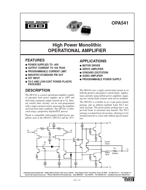
2®OPA541SPECIFICATIONSELECTRICALAt T C = +25°C and V S = ±35VDC, unless otherwise noted.OPA541AM/APOPA541BM/SM PARAMETERCONDITIONSMINTYP MAX MINTYP MAX UNITS INPUT OFFSET VOLTAGE V OS±2±10±0.1±1mV vs Temperature Specified Temperature Range±20±40±15±30µV/°C vs Supply Voltage V S = ±10V to ±V MAX±2.5±10T T µV/V vs Power±20±60T T µV/W INPUT BIAS CURRENT I B450T T pA INPUT OFFSET CURRENT I OS±1±30T TpA Specified Temperature Range5T nA INPUT CHARACTERISTICS Common-Mode Voltage Range Specified Temperature Range±(|V S | – 6)±(|V S | – 3)T T V Common-Mode Rejection V CM = (|±V S | – 6V)95113TT dB Input Capacitance 5T pF Input Impedance, DC 1T T ΩGAIN CHARACTERISTICS Open Loop Gain at 10Hz R L = 6Ω9097TT dB Gain-Bandwidth Product 1.6T MHz OUTPUTVoltage SwingI O = 5A, Continuous±(|V S | – 5.5)±(|V S | – 4.5)T T V I O = 2A ±(|V S | – 4.5)±(|V S | – 3.6)T T V I O = 0.5A±(|V S | – 4)±(|V S | – 3.2)T T V Current, Peak 910T T A AC PERFORMANCE Slew Rate610T T V/µs Power Bandwidth R L = 8Ω, V O = 20Vrms4555TT kHz Settling Time to 0.1%2V Step2Tµs Capacitive Load Specified Temperature Range, G = 1 3.3T nF Specified Temperature Range, G >10SOA (1)T Phase MarginSpecified Temperature Range, R L = 8Ω40T Degrees POWER SUPPLYPower Supply Voltage, ±V S Specified Temperature Range±10±30±35T±35±40V Current, Quiescent 2025TTmA THERMAL RESISTANCE θJC (Junction-to-Case)(2)AC Output f > 60Hz2.5°C/W θJC (2)DC Output 3°C/W θJA (Junction-to-Ambient)No Heat Sink40°C/W OPA541AP (Plastic)40°C/W TEMPERATURE RANGE T CASEAM, BM, AP–25+85T T °C SM–55+125°CT Specification same as OPA541AM/AP.NOTE: (1) SOA is the Safe Operating Area shown in Figure 1. (2) Plastic package may require insulator which typically adds 1°C/W.The information provided herein is believed to be reliable; however, BURR-BROWN assumes no responsibility for inaccuracies or omissions. BURR-BROWN assumes no responsibility for the use of this information, and all use of such information shall be entirely at the user’s own risk. Prices and specifications are subject to change without notice. No patent rights or licenses to any of the circuits described herein are implied or granted to any third party. BURR-BROWN does not authorize or warrant any BURR-BROWN product for use in life support devices and/or systems.3®OPA541CONNECTION DIAGRAMSORDERING INFORMATIONTEMPERATURECONTINUOUS PRODUCT PACKAGE RANGE CURRENT OPA541AP Power Plastic–25°C to +85°C 5A at 25°C OPA541AM TO-3–25°C to +85°C 5A at 25°C OPA541BM TO-3–25°C to +85°C 5A at 25°C OPA541SMTO-3–55°C to +125°C5A at 25°CABSOLUTE MAXIMUM RATINGSSupply Voltage, +V S to –V S ...............................................................80V Output Current.............................................................................see SOA Power Dissipation, Internal (1)...........................................................125W Input Voltage: Differential ....................................................................±V SCommon-mode.............................................................±V STemperature: Pin solder, 10s........................................................+300°CJunction (1)...............................................................+150°CTemperature Range:AM, BM SMStorage ....................................................................–65°C to +150°C Operating (case)......................................................–55°C to +125°C APStorage ......................................................................–40°C to +85°C Operating (case)........................................................–25°C to +85°C NOTE: (1) Long term operation at the maximum junction temperature will result in reduced product life. Derate internal power dissipation to achieve high MTTF.PACKAGE INFORMATIONPACKAGE DRAWINGPRODUCT PACKAGE NUMBER (1)OPA541AP Power Plastic242OPA541AM TO-3030OPA541BM TO-3030OPA541SMTO-3030NOTE: (1) For detailed drawing and dimension table, please see end of data sheet, or Appendix C of Burr-Brown IC Data Book.This integrated circuit can be damaged by ESD. Burr-Brown recommends that all integrated circuits be handled with appropriate precautions. Failure to observe proper handling and installation procedures can cause damage.ESD damage can range from subtle performance degradation to complete device failure. Precision integrated circuits may be more susceptible to damage because very small parametric changes could cause the device not to meet its published specifications.4®OPA5411010.10.010.001101001k 10k100kFrequency (Hz)T H D + N o i s e (%)TOTAL HARMONIC DISTORTION + NOISEvs FREQUENCY1k10010V o l t a g e N o i s e D e n s i t y (n V /√Hz )VOLTAGE NOISE DENSITYvs FREQUENCY1101001k10k100kFrequency (Hz)6543210012345678910I (A)OUT|±V | – |V | (V )OU T S OUTPUT VOLTAGE SWING vs OUTPUT CURRENT1.31.21.110.90.80.70.62030405060708090+V + |–V | (V)S SN o r m a l i z ed I NORMALIZED QUIESCENT CURRENT vs TOTAL POWER SUPPLY VOLTAGEQ1109070503010–101101001k 10k 100k 1M 10MFrequency (Hz)V o l t a g e G a i n (d B )OPEN-LOOP GAIN AND PHASEvs FREQUENCY–45–90–135–180P h a s e (D e g r e e s )–2502550751001251001010.10.010.001I n p u t B i as C u r r e n t (n A )Temperature (°C)INPUT BIAS CURRENT vs TEMPERATURETYPICAL PERFORMANCE CURVESAt T A = +25°C, V S = ±35VDC, unless otherwise noted.5®OPA5411201101009080706050101001k10k100k1MFrequency (Hz)C M R R (d B )COMMON-MODE REJECTIONvs FREQUENCY1010.10.010.1110R ( )ΩCL I (A )L I M I TCURRENT LIMIT vs RESISTANCE LIMITTYPICAL PERFORMANCE CURVES (CONT)At T A = +25°C, V S = ±35VDC, unless otherwise noted.Time (1µs/division)DYNAMIC RESPONSEV o l t a g e (2V /d i v i s i o n)1010.10.010.1110R ( )ΩCL I (A )L I M I TCURRENT LIMIT vs RESISTANCE LIMITvs TEMPERATURE6®OPA541θHS =T CASE – T AMBIENTP D (max)INSTALLATION INSTRUCTIONSPOWER SUPPLIESThe OPA541 is specified for operation from power supplies up to ±40V. It can also be operated from unbalanced power supplies or a single power supply, as long as the total power supply voltage does not exceed 80V. The power supplies should be bypassed with low series impedance capacitors such as ceramic or tantalum. These should be located as near as practical to the amplifier’s power supply pins. Good power amplifier circuit layout is, in general, like good high frequency layout. Consider the path of large power supply and output currents. Avoid routing these connections near low-level input circuitry to avoid waveform distortion and oscillations.CURRENT LIMITInternal current limit circuitry is controlled by a single external resistor, R CL . Output load current flows through this external resistor. The current limit is activated when the voltage across this resistor is approximately a base-emitter turn-on voltage. The value of the current limit resistor is approximately:(AM, BM, SM)R CL =– 0.057(AP)R CL =– 0.020.809|I LIM |0.813|I LIM |Because of the internal structure of the OPA541, the actual current limit depends on whether current is positive or negative. The above R CL gives an average value. For a given R CL , +I OUT will actually be limited at about 10% below the expected level, while –I OUT will be limited about 10% above the expected level.The current limit value decreases with increasing tempera-ture due to the temperature coefficient of a base-emitter junction voltage. Similarly, the current limit value increases at low temperatures. Current limit versus resistor value and temperature effects are shown in the Typical Performance Curves. Approximate values for R CL at other temperatures may be calculated by adjusting R CL as follows:The adjustable current limit can be set to provide protection from short circuits. The safe short-circuit current depends on power supply voltage. See the discussion on Safe Operating Area to determine the proper current limit value.Since the full load current flows through R CL , it must be selected for sufficient power dissipation. For a 5A current limit on the TO-3 package, the formula yields an R CL of 0.105Ω (0.143Ω on the power plastic package due to differ-ent internal resistances). A continuous 5A through 0.105Ωwould require an R CL that can dissipate 2.625W.∆R CL =x (T – 25)–2mV|I LIM |Sinusoidal outputs create dissipation according to rms load current. For the same R CL , AC peaks would still be limited to 5A, but rms current would be 3.5A, and a current limiting resistor with a lower power rating could be used. Some applications (such as voice amplification) are assured of signals with much lower duty cycles, allowing a current resistor with a low power rating. Wire-wound resistors may be used for R CL . Some wire-wound resistors, however, have excessive inductance and may cause loop-stability prob-lems. Be sure to evaluate circuit performance with resistor type planned for production to assure proper circuit opera-tion.HEAT SINKINGPower amplifiers are rated by case temperature, not ambient temperature as with signal op amps. Sufficient heat sinking must be provided to keep the case temperature within rated limits for the maximum ambient temperature and power dissipation. The thermal resistance of the heat sink required may be calculated by:Commercially available heat sinks often specify their ther-mal resistance. These ratings are often suspect, however,since they depend greatly on the mounting environment and air flow conditions. Actual thermal performance should be verified by measurement of case temperature under the required load and environmental conditions.No insulating hardware is required when using the TO-3package. Since mica and other similar insulators typically add approximately 0.7°C/W thermal resistance, their elimi-nation significantly improves thermal performance. See Burr-Brown Application Bulletin AB-038 for further details on heat sinking. On the power plastic package, the metal tab is connected to –V S , and appropriate actions should be taken when mounting on a heat sink or chassis.SAFE OPERATING AREAThe safe operating area (SOA) plot provides comprehensive information on the power handling abilities of the OPA541.It shows the allowable output current as a function of the voltage across the conducting output transistor (see Figure 1). This voltage is equal to the power supply voltage minus the output voltage. For example, as the amplifier output swings near the positive power supply voltage, the voltage across the output transistor decreases and the device can safely provide large output currents demanded by the load.7®OPA541FIGURE 1. Safe Operating Area.Short circuit protection requires evaluation of SOA. Whenthe amplifier output is shorted to ground, the full power supply voltage is impressed across the conducting output transistor. The current limit must be set to a value which is safe for the power supply voltage used. For instance, with V S ±35V, a short to ground would force 35V across the conduc-ting power transistor. A current limit of 1.8A would be safe.Reactive, or EMF-generating, loads such as DC motors can present difficult SOA requirements. With a purely reactive load, output voltage and load current are 90° out of phase.Thus, peak output current occurs when the output voltage is zero and the voltage across the conducting transistor is equal to the full power supply voltage. See Burr-Brown Applica-tion Bulletin AB-039 for further information on evaluating SOA.REPLACING HYBRID POWER AMPLIFIERSThe OPA541 can be used in applications currently using various hybrid power amplifiers, including the OPA501,OPA511, OPA512, and 3573. Of course, the application must be evaluated to assure that the output capability and other performance attributes of the OPA541 meet the neces-sary requirement. These hybrid power amplifiers use two current limit resistors to independently set the positive and negative current limit value. Since the OPA541 uses only one current limit resistor to set both the positive and negative current limit, only one resistor (see Figure 4) need be installed. If installed, the resistor connected to pin 2 (TO-3package) is superfluous, but it does no harm.Because one resistor carries the current previously carried by two, the resistor may require a higher power rating.Minor adjustments may be required in the resistor value to achieve the same current limit value. Often, however, the change in current limit value when changing models is small compared to its variation over temperature. Many applica-tions can use the same current limit resistor.FIGURE 3. Isolating Capacitive Loads.APPLICATIONS CIRCUITSFIGURE 2. Clamping Output for EMF-Generating Loads.FIGURE 4. Replacing OPA501 with OPA541.8®OPA541FIGURE 5. Paralleled Operation, Extended SOA.FIGURE 6. Programmable Voltage Source.FIGURE 7. 16-Bit Programmable Voltage Source.。
- 1、下载文档前请自行甄别文档内容的完整性,平台不提供额外的编辑、内容补充、找答案等附加服务。
- 2、"仅部分预览"的文档,不可在线预览部分如存在完整性等问题,可反馈申请退款(可完整预览的文档不适用该条件!)。
- 3、如文档侵犯您的权益,请联系客服反馈,我们会尽快为您处理(人工客服工作时间:9:00-18:30)。
54FCT541Octal Buffer/Line Driver with TRI-STATE ®OutputsGeneral DescriptionThe ’FCT541is an octal buffer and line driver with TRI-STATE outputs designed to be employed as a memory and address driver,clock driver,or bus-oriented transmitter/receiver.The ’FCT541is similar to the ’FCT244with broad-side pinout.Featuresn Non-inverting buffersn TTL input and output level compatible n CMOS power consumptionnOutput sink capability of 48mA,source capability of 12mAn Flow-through pinout for ease of PC board layout n Standard Microcircuit Drawing (SMD)5962-8976601Ordering CodeMilitaryPackage Package DescriptionNumber 54FCT541DMQB J20A 20-Lead Ceramic Dual-In-Line 54FCT541FMQB W20A 20-Lead Cerpack54FCT541LMQBE20A20-Lead Ceramic Leadless Chip Carrier,Type CConnection DiagramPin Names DescriptionOE 1,OE 2Output Enable Input (Active Low)I 0–I 7Inputs O 0–O 7Outputs Inputs Outputs OE 1OE 2I FCT541L L H H H X X Z X H X Z LLLLH =HIGH Voltage Level L =LOW Voltage Level X =ImmaterialZ =High ImpedanceTRI-STATE ®is a registered trademark of FAirchild Semiconductor Corporation.Pin Assignment DIP and CerpackDS100953-1Pin AssignmentLCCDS100953-30October 199954FCT541Octal Buffer/Line Driver with TRI-STATE Outputs©1999National Semiconductor Corporation Absolute Maximum Ratings (Note 1)If Military/Aerospace specified devices are required,please contact the National Semiconductor Sales Office/Distributors for availability and specifications.Storage Temperature−65˚C to +150˚C Ambient Temperature under Bias −55˚C to +125˚C Junction Temperature under Bias Ceramic−55˚C to +175˚C V CC Pin Potential to Ground Pin−0.5V to +7.0V Input Voltage (Note 2)−0.5V to +7.0V Input Current (Note 2)−30mA to +5.0mAVoltage Applied to Any Output in the Disabled or Power-Off State−0.5V to 5.5Vin the HIGH State−0.5V to V CCCurrent Applied to Output in LOW State (Max)twice the rated I OL (mA)DC Latchup Source Current−500mARecommended Operating ConditionsFree Air Ambient Temperature Military−55˚C to +125˚C Supply Voltage Military+4.5V to +5.5VMinimum Input Edge Rate (∆V/∆t)Data Input 50mV/ns Enable Input20mV/nsDC Electrical CharacteristicsSymbol ParameterFCT541UnitsV CCConditionsMinTypMaxV IH Input HIGH Voltage 2.0V Recognized HIGH Signal V IL Input LOW Voltage 0.8V Recognized LOW Signal V CD Input Clamp Diode Voltage −1.2V Min I IN =−18mA V OH Output HIGH Voltage 54FCT 4.3V Min I OH =−300µA 54FCT 2.4V Min I OH =−12mA V OL Output LOW Voltage 54FCT 0.2V Min I OL =300µA 54FCT0.55V Min I OL =48mA I IH Input HIGH Current 5µA Max V IN =V CCI IL Input LOW Current −5µA Max V IN =0.0VI OZH Output Leakage Current 10µA Max V OUT =5.5V;OE n =2.0V I OZL Output Leakage Current −10µA Max V OUT =0.0V;OE n =2.0V I OS Output Short-Circuit Current -60mA Max V OUT =0.0VI CCQ Quiescent Power Supply Current 1.5mA Max V IN <0.2V or V IN 5.3V,V CC =5.5V∆I CC Quiescent Power Supply Current 2.0mA Max V I =V CC −2.1VI CCDDynamic I CC0.4mA/MHz MaxV CC =5.5V,Outputs Open,One Bit Toggling,50%Duty Cycle,OE n =GNDI CCTotal Power Supply Current6.0mAMaxV CC =5.5V,Outputs Open,fI =10MHz,OE n =GND,One Bit Toggling,50%Duty Cycle,OE n =GNDNote 1:Absolute maximum ratings are values beyond which the device may be damaged or have its useful life impaired.Functional operation under these conditions is not implied.Note 2:Either voltage limit or current limit is sufficient to protect inputs.54F C T 541 2AC Electrical Characteristics54FCTT A=−55˚C to+125˚C Fig. Symbol Parameter V CC=4.5V–5.5V Units No.C L=50pFMin Maxt PLH Propagation Delay 2.09.0ns Figure4t PHL Data to Outputs 2.09.0t PZH Output Enable Time 2.012.5ns Figure5t PZL 2.012.5t PHZ Output Disable Time 2.012.5ns Figure5t PLZ 2.012.5CapacitanceSymbol Parameter Max Units ConditionsT A=25˚CC IN Input Capacitance10.0pF V CC=0.0VC OUT(Note3)Output Capacitance12.0pF V CC=5.0VNote3:C OUT is measured at frequency of f=1MHz,per MIL-STD-883B,Method3012.54FCT5413AC LoadingAC WaveformsDS100953-3*Includes jig and probe capacitanceFIGURE 1.Standard AC Test LoadDS100953-4FIGURE 2.Test Input Signal LevelsAmplitude Rep.Rate t w t r t f 3.0V1MHz500ns2.5ns2.5nsFIGURE 3.Test Input Signal RequirementsDS100953-5FIGURE 4.Propagation Delay Waveforms forInverting and Non-Inverting FunctionsDS100953-7FIGURE 5.TRI-STATE Output HIGH and LOWEnable and Disable Time54F C T 541 4Physical Dimensionsinches (millimeters)unless otherwise noted20-Terminal Ceramic Chip CarrierNS Package Number E20A20-Lead Ceramic Dual-In-Line PackageNS Package Number J20A54FCT5415Physical Dimensions inches(millimeters)unless otherwise noted(Continued)LIFE SUPPORT POLICYNATIONAL’S PRODUCTS ARE NOT AUTHORIZED FOR USE AS CRITICAL COMPONENTS IN LIFE SUPPORT DEVICES OR SYSTEMS WITHOUT THE EXPRESS WRITTEN APPROVAL OF THE PRESIDENT AND GENERAL COUNSEL OF NATIONAL SEMICONDUCTOR CORPORATION.As used herein:1.Life support devices or systems are devices orsystems which,(a)are intended for surgical implantinto the body,or(b)support or sustain life,andwhose failure to perform when properly used inaccordance with instructions for use provided in thelabeling,can be reasonably expected to result in asignificant injury to the user.2.A critical component is any component of a lifesupport device or system whose failure to performcan be reasonably expected to cause the failure ofthe life support device or system,or to affect itssafety or effectiveness.National SemiconductorCorporationAmericasTel:1-800-272-9959Fax:1-800-737-7018Email:support@National SemiconductorEuropeFax:+49(0)180-5308586Email:europe.support@Deutsch Tel:+49(0)180-5308585English Tel:+49(0)180-5327832Français Tel:+49(0)180-5329358Italiano Tel:+49(0)180-5341680National SemiconductorAsia Pacific CustomerResponse GroupTel:65-2544466Fax:65-2504466Email:sea.support@National SemiconductorJapan Ltd.Tel:81-3-5639-7560Fax:81-3-5639-7507 20-Lead Ceramic FlatpackNS Package Number W20A54FCT541OctalBuffer/LineDriverwithTRI-STATEOutputsNational does not assume any responsibility for use of any circuitry described,no circuit patent licenses are implied and National reserves the right at any time without notice to change said circuitry and specifications.。