IPD15N06S2L-64中文资料
2N06L64-NMOS管资料
0 -60 -20 20 60 100 140 180
T j [°C]
T j [°C]
11 Typ. capacitances C = f(V DS); V GS = 0 V; f = 1 MHz
12 Typical forward diode characteristicis IF = f(VSD) parameter: T j
Rev. 1.0
page 1
2006-07-18
IPD15N06S2L-64
Parameter
Symbol
Conditions min.
Values typ. max.
Unit
Thermal characteristics Thermal resistance, junction - case Thermal resistance, junction ambient, leaded SMD version, device on PCB R thJC R thJA R thJA minimal footprint 6 cm2 cooling area2) Electrical characteristics, at T j=25 °C, unless otherwise specified Static characteristics Drain-source breakdown voltage Gate threshold voltage Zero gate voltage drain current V (BR)DSS V GS=0 V, I D= 1 mA V GS(th) I DSS V DS=V GS, I D=14 µA V DS=55 V, V GS=0 V, T j=25 °C V DS=55 V, V GS=0 V, T j=125 °C1) Gate-source leakage current Drain-source on-state resistance Drain-source on-state resistance I GSS R DS(on) RDS(on) V GS=20 V, V DS=0 V V GS=4.5 V, I D=13 A V GS=10 V, I D=13 A 55 1.2 1.6 0.01 2.0 1 µA V 3.2 100 75 50 K/W
技术服务手册-PS篇(标准版)
第一章
一、特点
1、一体化设计,位置变送器、伺服放大器内装,调校方便。
2、结构简单,体积小巧,重量轻,便于安装维护。
3、采用精密小间隙密封齿轮传动,传动效率高,噪声低,寿命长,稳定性高,无需加油。
X2:执行器电机连接端子,连线方式参考图1。
X3:控制信号输入与位置信号输出端子,该端子标有3、4号的为控制信号输入端子,标有5、6号的为位置信号输出端子,连线方式参考图1。
X5:执行器位置电位器接线端子,连接方式参考图1。在按图示连接方式连接时,应确保执行器的电位器与电机板上端子X0的连接关系如图2所示。
接线如下图:其中X5/1为电机的如下图:
公共端,X5/2为电机开方向的L1
端,X54为电机关方向的L2端。
四、独立位置变送器接线
第四章
一、 限位开关的调整
二、伺服放大板PSAP5调试说明书
1、安全事项
调试过程中不可触摸电路板上导体部分,以防触电。
确保各接线端子正确连接。
2、接线端子介绍
X1:电源端子。
PS+POT+PSMF2DC
开关(24V直流电源)动作模式,输出4--20mA反馈信号
调节型
PS+POT+MSC305+MSC308
调节动作模式,输入/出4--20mA反馈信号
PS+POT+PSAP4C
四、PS反馈齿轮的直径与行程
直径(mm)
H行程(mm)
10.8
H=25(塑料)
IEC61215 标准 (中文版)[1]
![IEC61215 标准 (中文版)[1]](https://img.taocdn.com/s3/m/4820797977232f60ddcca177.png)
IEC61215 标准(中文版)美国光伏检测室( ASU-PTL)中国全权代理Solspring International Energy Group太阳普林国际能源集团(加拿大)2005年中国目的1。
决定组件的电性能和热性能。
2。
表明组件在合理的成本和时间内,能够承受长时间的气候暴露。
取样根据 IEC 60410 标准,8块用于质量测试的组件应从一批或几批产品中任意抽取。
通过的标准:1。
最大输出 (The degradation of Max. output power does not exceedthe prescribed limit after each test nor 8% after each test sequence)2。
电路 (no sample has exhibited any open-circuit during the tests)3。
目测迹象(There is no visual evidence of a major defect) 4。
绝缘性(The insulation test requirements are met after the tests)5。
湿漏电 (The wet leakage current test requirements are met at thebeginning and the end of each sequence and after the damp heat test)6。
特殊要求(Specific requirements of the individual tests are met)5kWh/m2目测,电性能,绝缘,湿漏1 12 22热循环 200电性能紫外线湿热热循环 50户外暴二极管热试验湿冻机械强度雹击热斑终端试验目测,电性能,绝缘,IEC61215 (第二版)标签每一个组件的标签都应包括以下内容且清楚可读:1. 生产厂商名字或标志。
CD74HC154M96E4,CD74HC154M96G4,CD74HC154M96,CD74HC154M96,CD74HC154M96, 规格书,Datasheet 资料
67
M (SOIC) Package (Note 2). . . . . . . . . . . . . . . . . . .
46Leabharlann Maximum Junction Temperature . . . . . . . . . . . . . . . . . . . . . . . 150oC
Maximum Storage Temperature Range . . . . . . . . . .-65oC to 150oC
1
芯天下--/
CD54HC154, CD74HC154, CD54HCT154, CD74HCT154
Functional Diagram
A0 23 A1 22 A2 21
20 A3
E1 18 E2 19
1 Y0
2 Y1
3 Y2
4 Y3
5 Y4
6 Y5
7 Y6
8 Y7
[ /Title (CD74 HC154 , CD74 HCT15 4) /Subject (High Speed CMOS Logic 4-to-16 Line Decod er/Dem
Features
• Two Enable Inputs to Facilitate Demultiplexing and Cascading Functions
Data sheet acquired from Harris Semiconductor SCHS152D
September 1997 - Revised June 2004
CD54HC154, CD74HC154, CD54HCT154, CD74HCT154
High-Speed CMOS Logic 4- to 16-Line Decoder/Demultiplexer
W25Q64中文资料精编版
W25Q64BV出版日期:2010年7月8日- 1 - 版本E64M位与串行闪存双路和四路SPIW25Q64BV- 2 -目录1,一般DESCRIPTION (5)2。
FEATURES (5)3引脚配置SOIC208-MIL.......................................... .. (6)4,焊垫配置WSON8X6-MM.......................................... . (6)5,焊垫配置PDIP300-MIL.......................................... . (7)6引脚说明SOIC208密耳,PDIP300密耳和WSON8X6-MM................................ 7......7引脚配置SOIC300mil的.......................................... .. (8)8引脚SOIC封装说明300-MIL (8)8.1包装Types (9)8.2片选(/CS) (9)8.3串行数据输入,输出和IO(DI,DO和IO0,IO1,IO2,IO3)............................. 9.......8.4写保护(/WP) (9)8.5控股(/HOLD) (9)8.6串行时钟(CLK) (9)9座DIAGRAM (10)10功能DESCRIPTION (11)10.1 SPI OPERATIONS (11)10.1.1标准SPI Instructions (11)10.1.2双SPI Instructions (11)10.1.3四路SPI Instructions (11)10.1.4保持功能 (11)10.2写保护 (12)10.2.1写保护Features (12)11,控制和状态寄存器............................................ .. (13)11.1状态REGISTER (13)11.1.1 BUSY (13)11.1.2写使能锁存(WEL) (13)11.1.3块保护位(BP2,BP1,BP0)..................................... .. (13)11.1.4顶/底块保护(TB)....................................... .................................................. ..1311.1.5部门/块保护(SEC) (13)11.1.6状态寄存器保护(SRP,SRP0)....................................... . (14)11.1.7四路启用(QE) (14)11.1.8状态寄存器内存保护........................................... .. (16)11.2 INSTRUCTIONS (17)11.2.1制造商和设备标识........................................... .. (17)11.2.2指令集表1 (18)W25Q64BV11.2.3指令表2(阅读说明书)....................................... (19)出版日期:2010年7月8日- 3 - 修订版E11.2.4写使能(06h) (20)11.2.5写禁止(04h) (20)11.2.6读状态寄存器1(05H)和读状态寄存器2(35H).............................. (21)11.2.7写状态寄存器(01H)......................................... .................................................. .. (22)11.2.8读取数据(03h) (23)11.2.9快速阅读(0Bh) (24)11.2.10快速读双输出(3BH)........................................ .................................................. 0.25 11.2.11快速读四路输出(6BH)........................................ .. (26)11.2.12快速读双I / O (BBh) (27)11.2.13快速读取四I/ O (EBh) (29)11.2.14八进制字读取四I/ O(E3H)..................................... (31)11.2.15页编程(02h) (33)11.2.16四路输入页编程(32H)........................................ . (34)11.2.17扇区擦除(20H) (35)11.2.1832KB的块擦除(52H) (36)11.2.1964KB的块擦除(D8h) (37)20年2月11日芯片擦除(C7H/ 60h) (38)21年2月11日擦除挂起(75h) (39)22年2月11日擦除恢复(7Ah) (40)23年11月2日掉电(B9h) (41)24年2月11日高性能模式(A3H)......................................... (42)25年2月11日发布掉电或高性能模式/设备ID(ABH) (42)26年2月11日读制造商/设备ID(90H)....................................... . (44)27年2月11日阅读唯一的ID号(4BH)........................................ . (45)28年2月11日读JEDEC的ID (9Fh) (46)29年2月11日连续读取模式复位(FFH或FFFFH)...................................... .. (47)12,电气特性.............................................. (48)12.1绝对最大Ratings (48)12.2操作范围 (48)12.3上电时序和写抑制阈值......................................... (49)12.4直流电气Characteristics (50)12.5 AC测量条件.............................................. .. (51)12.6 AC电气Characteristics (52)12.7 AC电气特性(续)......................................... . (53)12.8串行输出Timing (54)12.9输入Timing (54)12.10持有Timing (54)13包装SPECIFICATION (55)W25Q64BV13.18引脚SOIC208密耳(包装代号SS)..................................... .. (55)- 4 -13.28引脚PDIP300密耳(封装代码DA)..................................... (56)13.38触点WSON8x6毫米(封装代码ZE)....................................... (57)13.416引脚SOIC300密耳(封装代码SF)..................................... . (58)14订货INFORMA TION (59)14.1有效的部件号和顶端标记.......................................... (60)15版本HISTORY (61)W25Q64BV出版日期:2010年7月8日- 5 - 修订版E1概述该W25Q64BV(64M位)串行Flash存储器提供了有限的系统存储解决方案空间,引脚和电源。
IPD640N06LG中文资料
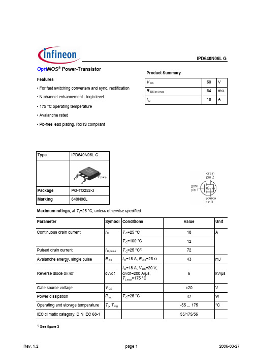
PG-TO252-3IPD640N06L GParameter Symbol Conditions Unitmin.typ.max. Thermal characteristicsThermal resistance, junction - case R thJC-- 3.2K/W SMD version, device on PCB R thJA minimal footprint--756 cm2 cooling area2)--50 Electrical characteristics, at T j=25 °C, unless otherwise specifiedStatic characteristicsDrain-source breakdown voltage V(BR)DSS V GS=0 V, I D=1 mA60--V Gate threshold voltage V GS(th)V DS=V GS, I D=16 µA 1.2 1.62Zero gate voltage drain current I DSS V DS=60 V, V GS=0 V,T j=25 °C-0.011µAV DS=60 V, V GS=0 V,T j=125 °C-1100Gate-source leakage current I GSS V GS=20 V, V DS=0 V-10100nA Drain-source on-state resistance R DS(on)V GS=10 V, I D=18 A-4764mΩV GS=4.5 V, I D=12 A-6485Gate resistance R G- 1.2-ΩTransconductance g fs |V DS|>2|I D|R DS(on)max,I D=18 A9.519-S2) Device on 40 mm x 40 mm x 1.5 mm epoxy PCB FR4 with 6 cm2 (one layer, 70 µm thick) copper area for drain connection. PCB is vertical in still air.ValuesIPD640N06L GParameterSymbol ConditionsUnitmin.typ.max.Dynamic characteristics Input capacitance C iss -350470pFOutput capacitanceC oss -94130Reverse transfer capacitance C rss -3553Turn-on delay time t d(on)-68ns Rise timet r -2538Turn-off delay time t d(off)-3248Fall timet f-3248Gate Charge Characteristics 3)Gate to source charge Q gs - 1.4 1.9nCGate charge at threshold Q g(th)-0.50.7Gate to drain charge Q gd - 3.6 5.4Switching charge Q sw - 4.5 6.5Gate charge total Q g -1013Gate plateau voltage V plateau - 4.2-V Output charge Q ossV DD =30 V, V GS =0 V -34Reverse DiodeDiode continous forward current I S --18ADiode pulse current I S,pulse --72Diode forward voltageV SDV GS =0 V, I F =18 A, T j =25 °C-0.991.3V Reverse recovery time t rr-3045nsReverse recovery charge Q rr -2030nC3)See figure 16 for gate charge parameter definitionV R =30 V, I F =I S , d i F /d t =100 A/µsT C =25 °CValues V GS =0 V, V DS =30 V, f =1 MHzV DD =30 V, V GS =10 V, I D =15 A, R G =22 ΩV DD =30 V, I D =18 A, V GS =0 to 10 V1 Power dissipation5 Typ. output characteristics9 Drain-source on-state resistance13 Avalanche characteristicsPG-TO252-3: Outline packaging:IPD640N06L GPublished byInfineon Technologies AG81726 München, Germany© Infineon Technologies AG 2006.All Rights Reserved.Attention please!The information given in this data sheet shall in no event be regarded as a guarantee of conditions ocharacteristics (“Beschaffenheitsgarantie”). With respect to any examples or hints given herein, any typical values stated herein and/or any information regarding the application of the device, Infineon Technologies herebydisclaims any and all warranties and liabilities of any kind, including without limitation warranties oInformationFor further information on technology, delivery terms and conditions and prices please contact your nearesInfineon Technologies Office ().WarningsDue to technical requirements components may contain dangerous substances. For information on the types in question please contact your nearest Infineon Technologies Office.Infineon Technologies Components may only be used in life-support devices or systems with the express written approval of Infineon Technologies, if a failure of such components can reasonably be expected to cause the failureof that life-support device or system, or to affect the safety or effectiveness of that device or system. Life support devices or systems are intended to be implanted in the human body, or to support and/or maintain and sustainand/or protect human life. If they fail, it is reasonable to assume that the health of the user or other persons maybe endangered.。
IXDR35N60BD1;中文规格书,Datasheet资料
times versus gate resistor
10 K/W
1 ZthJC
0.1
0.01
single pulse
diode IGBT
0.001
0.0001 10-5
10-4
10-3
10-2
10-1 t
IXDR30N60BD1
100 s 101
Fig. 12 Typ. transient thermal impedance
600
V
600
V
±20
V
±30
V
38
A
24
A
48
A
ICM = 110
A
VCEK < VCES
10
µs
125
W
50
W
-55 ... +150
°C
-55 ... +150
°C
2500
V~
20...120
N
6
g
Conditions
V =0V GE
IC = 0.7 mA, VCE = VGE VCE = VCES
V = 0 V, V = ± 20 V
CE
GE
IC = 35 A, VGE = 15 V
Characteristic Values
(TJ = 25°C, unless otherwise specified) min. typ. max.
600
V
3
5V
TJ = 25°C TJ = 125°C
0.1 mA
VGE(th) ICES
I
GES
VCE(sat)
Conditions
IAP15W4K61S4单片机部分特殊功能寄存器(精品文档)_共3页
PSW:位号B7B6B5B4B3B2B1B0符号CY AC F0RS1RS0OV F1P辅助寄存器AUXR(地址为8EH,复位值为01H):位号B7B6B5B4B3B2B1B0位名称T0x12T1x12UART_M0x6T2R T2_C/T T2x12EXTRAM S1ST2I/O口工作模式设置寄存器PnM1[7:0]PnM0[7:0]I/O口模式00准双向口(传统8051单片机I/O口模式)01推挽输出10仅为输入(高阻)11开漏(Open Drain),内部上拉电阻断开,要外加上拉电阻辅助寄存器AUXR1(地址为A2H,复位值为0000 0000B)和外设功能切换寄存器P_SW2(地址为BAH,复位值为xxxx xxx0B)位号寄存器B7B6B5B4B3B2B1B0AUXR1S1_S1S1_S0CCP_S1CCP_S0SPI_S1SPI_S00DPSP_SW2PWM67_S PWM2345_S S4_S S3_S S2_SCLK_DIV SYSCKO_S1SYSCKO_S0ADRJ Tx_Rx SYSCLKO_2CLKS2CLKS1CLKS0INT_CLKO EX4EX3EX2SYSCKO_S2T2CLKO T1CLKO T0CLKOTCON(地址为88H,复位值为00H)位号B7B6B5B4B3B2B1B0位名称TF1TR1TF0TR0IE1IT1IE0IT0 SCON(地址为98H,复位值为00H)位号B7B6B5B4B3B2B1B0位名称SM0/FE SM1SM2REN TB8RB8TI RIS2CON(地址为9AH,复位值为00H)位号B7B6B5B4B3B2B1B0位名称S2SM0-S2SM2S2REN S2TB8S2RB8S2TI S2RI串口3控制寄存器S3CON(地址为ACH,复位值为40H)位号B7B6B5B4B3B2B1B0位名称S3SM0S3ST3S3SM2S3REN S3TB8S3RB8S3TI S3RI串口4控制寄存器S4CON(地址为84H,复位值为00H)位号B7B6B5B4B3B2B1B0位名称S4SM0S4ST4S4SM2S4REN S4TB8S4RB8S4TI S4RI电源控制寄存器PCON(地址为87H,复位值为30H)位号B7B6B5B4B3B2B1B0位名称SMOD SMOD0LVDF POF GF1GF0PD IDL CCON(地址为D8H,复位值为00xx x000B)位号B7B6B5B4B3B2B1B0位名称CF CR---CCF2CCF1CCF0SPSTAT(地址为CDH,复位值为00xx xxxxB)位号B7B6B5B4B3B2B1B0位名称SPIF WCOL------ADC控制寄存器ADC_CONTR(地址为BCH,复位值为00H)位号B7B6B5B4B3B2B1B0位名称ADC_POWER SPEED1SPEED0ADC_FLAG ADC_START CHS2CHS1CHS0中断允许寄存器IE(地址为A8H,复位值为00H)位号B7B6B5B4B3B2B1B0位名称EA ELVD EADC ES ET1EX1ET0EX0中断允许寄存器IE2(地址为AFH,复位值为xxxx x000B)位号B7B6B5B4B3B2B1B0位名称-ET4ET3ES4ES3ET2ESPI ES2外部中断使能和时钟输出寄存器INT_CLKO(地址为8FH,复位值为x000x000B)位号B7B6B5B4B3B2B1B0位名称-EX4EX3EX2MCKO_S2T2CLKO T1CLKO T0CLKO中断优先级寄存器IP(地址为B8H,复位值为00H)位号B7B6B5B4B3B2B1B0位名称PPCA PLVD PADC PS PT1PX1PT0PX0第二中断优先级寄存器IP2(地址为B5H,复位值为xxx0 0000B)位号B7B6B5B4B3B2B1B0位名称---PX4PPWMFD PPWM PSPI PS2TMOD(地址为89H,复位值为00H)位号B7B6B5B4B3B2B1B0定时器名定时器1定时器0位名称GATE C/T M1M0GATE C/T M1M0T4和T3控制寄存器T4T3M(地址为D1H,复位值为00H)位号B7B6B5B4B3B2B1B0位名称TR4T4_C/T T4x12T4CLKO TR3T3_C/T T3x12T3CLKOT0重装值寄存器高字节TH0(地址为8CH)、T0重装值寄存器低字节TL0(地址为8AH)、T1重装值寄存器高字节TH1(地址为8DH)、T1重装值寄存器低字节TL1(地址为8BH)、T2重装值寄存器高字节TH2(地址为D6H)、T2重装值寄存器低字节TL2(地址为D7H)、T3重装值寄存器高字节TH3(地址为D4H)、T3重装值寄存器低字节TL3(地址为D5H)、T4重装值寄存器高字节TH4(地址为D2H)、T4重装值寄存器低字节TL4(地址为D3H)时钟分频寄存器CLK_DIV(地址为97H,复位值为0000 x000B)位号B7B6B5B4B3D2D1D0位名称MCKO_S1MCKO_S0ADRJ TX_RX-CLKS2CLKS1CLKS0SPI控制寄存器SPCTL(地址为CEH,复位值为0000 0100B)位号B7B6B5B4B3B2B1B0位名称SSIG SPEN DORD MSTR CPOL CPHA SPR1SPR0SPI数据寄存器SPDAT(地址为CFH,复位值为00H)位号B7B6B5B4B3B2B1B0位名称MSB LSBP1ASF(地址为9DH,复位值为00H)位号B7B6B5B4B3B2B1B0位名称P17ASF P16ASF P15ASF P14ASF P13ASF P12ASF P11ASF P10ASFA/D转换结果寄存器ADC_RES(地址为BDH,复位值为00H)和ADC_RESL(地址为BEH,复位值为00H)IAP15W4K61S4单片机的中断源及其相关控制中断源中断入口地址默认中断优先级次序号优先级设置相关位低优先级高优先级中断请求标志位中断允许控制位外部中断INT00003H0(最高)PX001IE0EX0/EA T0溢出中断000BH1PT001TF0ET0/EA 外部中断INT10013H2PX101IE1EX1/EA T1溢出中断001BH3PT101TF1ET1/EA 串口1UART10023H4PS01RI + TI ES/EA ADC002BH5PADC01ADC_FLAG EADC/EA LVD0033H6PLVD01LVDF ELVD/EAPCA003BH7PPCA01CF+CCF0+CCF1(ECF+ECCF0+ECCF1)/EA串口2UART20043H8PS201S2RI+S2TI ES2/EA SPI004BH9PSPI01SPIF ESPI/EA外部中断INT20053H100EX2/EA外部中断INT3005BH110EX3/EA T2溢出中断0063H120ET2/EA外部中断INT40083H160EX4/EA 串口3中断008BH170ES3/EA 串口4中断0093H180ES4/EA T3溢出中断009BH190ET3/EA T4溢出中断00A3H200ET4/EA 比较器中断00ABH210(PIE+NIE)/EA PWM中断00B3H22PPWM01CBIF(EPWM+ECBI)/EA PWM异常检测中断00BBH23(最低)PPWMFD01FDIF(EPWM+EFD+EFDI)/EA常用波特率与系统时钟及重装时间常数之间的关系时钟频率/MHz分频模式波特率/bit/s时间常数高字节(THn)时间常数低字节(TLn)19200FFH F4H9600FFH E8H11.059212T4800FFH D0HOCM4X8C液晶显示模块基本命令集控制引脚控制命令RS R/W E D7D6D5D4D3D2D1D0功能00100000001消除显示0010000001*地址归位(复位到0x00)001000001I/D S进入点设定00100001D C B显示状态控制0010001S/C R/L**游标或显示移位控制001001DL*RE**功能设定00101AC5AC4AC3AC2AC1AC0设置CGRAM地址0011AC6AC5AC4AC3AC2AC1AC0设置DDRAM地址011BF AC6AC5AC4AC3AC2AC1AC0读忙标志或地址101D7D6D5D4D3D2D1D0写数到内部RAM111D7D6D5D4D3D2D1D0从内部RAM读取数据表8-5 OCM4X8C液晶显示模块扩充命令集控制引脚控制命令RS R/W E D7D6D5D4D3D2D1D0功能00100000001待命模式(DDRAM填满0x20,光标复位到0x00)0010000001SR卷动地址或IRAM地址选择001000001R1R2反白选择图8-7 OCM4X8C外形图00100001SL**睡眠模式0010001*1REG0扩充功能设定00101AC5AC4AC3AC2AC1AC0设定IRAM地址或卷动地址0010AC6AC5AC4AC3AC2AC1AC0设定绘图RAM地址图8 128x64液晶串行接口方式的时序图。
- 1、下载文档前请自行甄别文档内容的完整性,平台不提供额外的编辑、内容补充、找答案等附加服务。
- 2、"仅部分预览"的文档,不可在线预览部分如存在完整性等问题,可反馈申请退款(可完整预览的文档不适用该条件!)。
- 3、如文档侵犯您的权益,请联系客服反馈,我们会尽快为您处理(人工客服工作时间:9:00-18:30)。
IPD15N06S2L-64
Parameter Symbol Conditions Unit
min.typ.max. Thermal characteristics
Thermal resistance, junction - case R thJC-- 3.2K/W Thermal resistance, junction -
ambient, leaded
R thJA--100
SMD version, device on PCB R thJA minimal footprint--75
6 cm2 cooling area2)--50 Electrical characteristics, at T j=25 °C, unless otherwise specified
Static characteristics
Drain-source breakdown voltage V(BR)DSS V GS=0 V, I D= 1 mA55--V Gate threshold voltage V GS(th)V DS=V GS, I D=14 µA 1.2 1.6 2.0
Zero gate voltage drain current I DSS V DS=55 V, V GS=0 V,
T j=25 °C
-0.011µA
V DS=55 V, V GS=0 V,
T j=125 °C1)
-1100
Gate-source leakage current I GSS V GS=20 V, V DS=0 V-1100nA Drain-source on-state resistance R DS(on)V GS=4.5 V, I D=13 A-6185mΩDrain-source on-state resistance R DS(on)V GS=10 V, I D=13 A -4764mΩ
Values
Parameter Symbol Conditions
Unit
min.
typ.
max.
Dynamic characteristics 1)Input capacitance C iss -354-pF
Output capacitance
C oss -103-Reverse transfer capacitance C rss -38-Turn-on delay time t d(on)-4-ns
Rise time
t r -14-Turn-off delay time t d(off)-21-Fall time
t f
-
12
-
Gate Charge Characteristics 1)Gate to source charge Q gs -1 1.5nC
Gate to drain charge Q gd -45Gate charge total Q g -1113Gate plateau voltage V plateau
-
3.8
-
V
Reverse Diode
Diode continous forward current 1)I S --19A
Diode pulse current
1)
I S,pulse --76Diode forward voltage V SD
V GS =0 V, I F =15 A, T j =25 °C -
0.93
1.3
V
Reverse recovery time 1)t rr V R =30 V, I F =I S , d i F /d t =100 A/µs -34-ns
Reverse recovery charge 1)Q rr V R =30 V, I F =I S , d i F /d t =100 A/µs
-32-nC
1) Defined by design. Not subject to production test.
2)
Device on 40 mm x 40 mm x 1.5 mm epoxy PCB FR4 with 6 cm 2 (one layer, 70 µm thick) copper area for drain connection. PCB is vertical in still air.
T C =25 °C
Values V GS =0 V, V DS =25 V, f =1 MHz
V DD =30 V, V GS =10 V, I D =15 A, R G =20 ΩV DD =44 V, I D =19 A, V GS =0 to 10 V
1 Power dissipation
5 Typ. output characteristics
9 Typ. Drain-source on-state resistance
13 Typical avalanche energy
Published by
Infineon Technologies AG
Am Campeon 1-12
D-85579 Neubiberg
© Infineon Technologies AG 1999
All Rights Reserved.
Attention please!
The information herein is given to describe certain components and shall not be considered as
a guarantee of characteristics.
Terms of delivery and rights to technical change reserved.
We hereby disclaim any and all warranties, including but not limited to warranties of non-infringement, regarding circuits, descriptions and charts stated herein.
Information
For further information on technology, delivery terms and conditions and prices, please contact your nearest Infineon Technologies Office ()
Warnings
Due to technical requirements, components may contain dangerous substances.
For information on the types in question, please contact your nearest Infineon Technologies Office. Infineon Technologies' components may only be used in life-support devices or systems with the expressed written approval of Infineon Technologies, if a failure of such components can reasonably be expected to cause the failure of that life-support device or system, or to affect the safety or effectiveness of that device or system. Life support devices or systems are intended to be implanted in the human body, or to support and/or maintain and sustain and/or protect human life. If they fail,
it is reasonable to assume that the health of the user or other persons may be endangered.。