CLS4D23NP-1R2N中文资料
杭州士兰微电子股份有限公司 SC7A20 三轴微机械数字加速度传感器说明书

±2G/±4G/±8G/±16G三轴微机械数字加速度计描述SC7A20是一款高精度12bit数字三轴加速度传感器芯片,内置功能更丰富,功耗更低,体积更小,测量更精确。
芯片通过I²C/SPI接口与MCU通信,加速度测量数据以中断方式或查询方式获取。
INT1和INT2中断管脚提供多种内部自动检测的中断信号,适应多种运动检测场合,中断源包括6D/4D方向检测中断信号、自由落体检测中断信号、睡眠和唤醒检测中断信号、单击和双击检测中断信号。
芯片内置高精度校准模块,对传感器的失调误差和增益误差进行精确补偿。
±2G、±4G、±8G和±16G四种可调整的全量程测量范围,灵活测量外部加速度,输出数据率1HZ和400HZ间可选。
芯片内置自测试功能允许客户系统测试时检测系统功能,省去复杂的转台测试。
芯片内置产品倾斜校准功能,对贴片和板卡安装导致的倾斜进行补偿,不占系统资源,系统文件升级不影响传感器参数。
主要特点宽电压范围1.71V-3.6V1.8V兼容数字IO口低功耗模式下电源电流低至2µA±2G/±4G/±8G/±16G动态全量程范围 12bit有效数据(HR)I²C/SPI数字输出接口6D/4D方向检测自由落体检测单击双击检测及运动检测可编程中断生成电路内嵌自测试功能内嵌FIFO10000g高G抗击能力应用手机平板室内导航图像旋转运动激活用户接口游戏产品规格分类产品名称 封装形式 打印名称 材料 包装形式 SC7A20TR LGA-12-2x2x1.0 SC7A20 无铅编带内部框图XY ZC-to-V Converter Gain数符号测试条件最小值V CC电路不损坏-0.3 3.6V P电路不损坏V in电路不损坏T OPR电路不损坏T STG电路不损坏(VDD=2.5V, T测试条件123FS=0 (HR mode)FS=1 (HR mode)FS=2 (HR mode)FS=3 (HR mode)参 数符 号测试条件最小值 典型值 最大值 单位 零漂 Ty Off0 FS =0 --±40--mg温漂TC Off 与25°C 的最大偏差 -- ±0.5 -- mg/°C 自测输出V st1FS=0, X 轴 -- 276 -- LSb V st2 FS=0, Y 轴 -- 276 -- LSb V st3FS=0, Z 轴-- 984 -- LSb 系统带宽 BW -- ODR/2 -- HZ 工作温度T OPR-40--+85°C注意:电路2.5V 出厂校准。
maxwell软件-三相感应电机
8三相感应电动机本章我们将简化RMxprt一些基本操作的介绍,以便介绍一些更高级的使用。
有关RMxprt基本操作的详细介绍请参考第一部分的章节。
8.1基本理论三相感应电机的定子绕组通常连接到对称的三相电源上。
定子绕组由p对极组成,在空间成正弦分布,定子电流产生旋转磁场。
转子绕组一般为鼠笼型,其极数与定子绕组保持一致。
转子导条中感应的电流反过来又产生一个旋转磁场,这两个旋转磁场在电机气隙中相互作用产生合成磁场。
气隙合成磁场与转子导条电流相互作用产生电磁转矩,使转子按磁场旋转的方向旋转,同时有一个大小相同方向相反的转矩反作用于定子上。
定子绕组分为p组线圈,每一组都按三相对称分布,在电机中占据n D/2P空间,此处D为气隙直径。
因而气隙磁场有p个周期,定子绕组具有p对极。
三相感应电动机的特性是基于等效电路进行分析的。
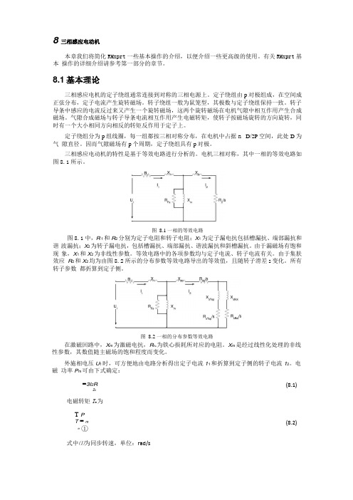
电机三相对称,其中一相的等效电路如图8.1所示。
图8.1中,R 1和R2分别为定子电阻和转子电阻;X1为定子漏电抗包括槽漏抗、端部漏抗和谐波漏抗;X2为转子漏电抗,包括槽漏抗、端部漏抗、谐波漏抗和斜槽漏抗。
由于漏磁场有饱和现象,X1和X2为非线性参数。
等效电路中的各项参数均与定子电流、转子电流有关。
由于集肤效应R2和X2均为由图8.2所示的分布参数等效电路导出的等效值,且随转子滑差s变化。
所有转子参数都折算到定子侧。
在激磁回路中,X m为激磁电抗,R Fe为铁心损耗所对应的电阻。
X m是经过线性化处理的非线性参数,其数值随主磁场的饱和程度而变化。
外施相电压U1时,可方便地由电路分析得出定子电流11和折算到定子侧的转子电流12。
电磁功率P m可由下式确定:=3I2R2s电磁转矩T m为T PT = mm①式中⑴为同步转速,单位:rad/s(8.1)(8.2)图8.1一相的等效电路图8.2 一相的分布参数等效电路轴端输出机械转矩为T2= T m - TW式中f 为风阻和摩擦转矩 输出功率为 P = T ①222式中巴=3(1-s )为转子转速,单位:rad/s 输入功率为P1= P2 +P加 +PCu2+PFe+九 +P(8.5)式中,尸彳风摩损耗,尸cu2为转子铜损耗,P Fe 为铁心损耗,P Cu1为定子铜损耗,P s 为杂散损耗。
FPGA可编程逻辑器件芯片EP4CE40F23I7N中文规格书
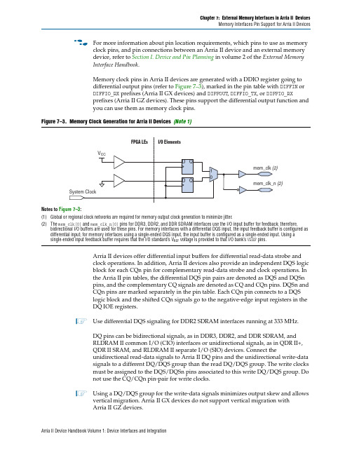
Chapter 7:External Memory Interfaces in Arria II DevicesMemory Interfaces Pin Support for Arria II Devicesf For more information about pin location requirements, which pins to use as memoryclock pins, and pin connections between an Arria II device and an external memorydevice, refer to Section I. Device and Pin Planning in volume 2 of the External MemoryInterface Handbook.Memory clock pins in Arria II devices are generated with a DDIO register going todifferential output pins (refer to Figure7–3), marked in the pin table with DIFFIN orDIFFIO_RX prefixes (Arria II GX devices) and DIFFOUT, DIFFIO_TX, or DIFFIO_RXprefixes (Arria II GZ devices). These pins support the differential output function andyou can use them as memory clock pins.Figure7–3.Memory Clock Generation for Arria II Devices(Note1)Notes to Figure7–3:(1)Global or regional clock networks are required for memory output clock generation to minimize jitter.(2)The mem_clk[0] and mem_clk_n[0] pins for DDR3, DDR2, and DDR SDRAM interfaces use the I/O input buffer for feedback; therefore,bidirectional I/O buffers are used for these pins. For memory interfaces with a differential DQS input, the input feedback buffer is configured as differential input; for memory interfaces using a single-ended DQS input, the input buffer is configured as a single-ended input. Using a single-ended input feedback buffer requires that the I/O standard’s V REF voltage is provided to that I/O bank’s VREF pins.Arria II devices offer differential input buffers for differential read-data strobe andclock operations. In addition, Arria II devices also provide an independent DQS logicblock for each CQn pin for complementary read-data strobe and clock operations. Inthe Arria II pin tables, the differential DQS pin pairs are denoted as DQS and DQSnpins, and the complementary CQ signals are denoted as CQ and CQn pins. DQSn andCQn pins are marked separately in the pin table. Each CQn pin connects to a DQSlogic block and the shifted CQn signals go to the negative-edge input registers in theDQ IOE registers.1Use differential DQS signaling for DDR2 SDRAM interfaces running at 333MHz.DQ pins can be bidirectional signals, as in DDR3, DDR2, and DDR SDRAM, andRLDRAM II common I/O (CIO) interfaces or unidirectional signals, as in QDR II+,QDR II SRAM, and RLDRAM II separate I/O (SIO) devices. Connect theunidirectional read-data signals to Arria II DQ pins and the unidirectional write-datasignals to a different DQ/DQS group than the read DQ/DQS group. The write clocksmust be assigned to the DQS/DQSn pins associated to this write DQ/DQS group. Donot use the CQ/CQn pin-pair for write clocks.1Using a DQ/DQS group for the write-data signals minimizes output skew and allows vertical migration. Arria II GX devices do not support vertical migration withArria II GZ devices.Arria II Device Handbook Volume 1: Device Interfaces and IntegrationChapter 6:I/O Features in Arria II DevicesTermination Schemes for I/O Standardsmini-LVDSArria II GX devices support true mini-LVDS with a three-resistor network using twosingle-ended output buffers for external three-resistor networks.For Arria II GZ devices, use two single-ended output buffers with external one- orthree-resistor networks (mini-LVDS_E_1R or mini-LVDS_E_3R). Arria II GZ row I/Obanks support mini-LVDS output using true LVDS output buffers without an externalresistor network.Figure6–18 shows the one-resistor and three-resistor topology for RSDS andmini-LVDS I/O standard termination.Figure6–18.RSDS and mini-LVDS I/O Standard Termination for Arria II Devices(Note1)Notes to Figure6–18:(1)R p = 170 Ω and R s= 120 Ω(2)mini-LVDS_E_1R is applicable for Arria II GZ devices only.A resistor network is required to attenuate the LVDS output-voltage swing to meetRSDS and mini-LVDS specifications. You can modify the three-resistor networkvalues to reduce power or improve the noise margin. The resistor values chosenshould satisfy the equation shown in Equation6–1.Equation6–1.Resistor Network1To validate that custom resistor values meet the RSDS requirements, Alterarecommends performing additional simulations with IBIS models.f For more information about the RSDS I/O standard, refer to the RSDS Specificationfrom the National Semiconductor website at .f For more information about the mini-LVDS I/O standard, see the mini-LVDSSpecification from the Texas Instruments website at .Arria II Device Handbook Volume 1: Device Interfaces and IntegrationChapter 6:I/O Features in Arria II DevicesArria II OCT CalibrationArria II OCT CalibrationArria II GX devices support calibrated R S OCT and Arria II GZ devices supportcalibrated R S and R T OCT on all I/O pins. You can calibrate the I/O banks with any ofthe OCT calibration blocks available in the device provided the V CCIO of the I/O bankwith the pins using calibrated OCT matches the V CCIO of the I/O bank with thecalibration block and its associated RUP and RDN pins.f For more information about the location of the OCT calibration blocks in Arria IIdevices, refer to the Arria II Device Family Connection Guidelines and Arria II DevicePin-Outs.OCT Calibration BlockAn OCT calibration block has the same V CCIO as the I/O bank that contains the block.R S OCT calibration is supported on all user I/O banks with different V CCIO voltagestandards, up to the number of available OCT calibration blocks. You can configureI/O banks to receive calibrated codes from any OCT calibration block with the sameV CCIO. All I/O banks with the same V CCIO can share one OCT calibration block, even ifthat particular I/O bank has an OCT calibration block.For example, Figure6–10 shows a group of I/O banks that has the same V CCIOvoltage. If a group of I/O banks has the same V CCIO voltage, you can use one OCTcalibration block to calibrate the group of I/O banks placed around the periphery.Because banks 3B, 4C, 6C, and 7B have the same V CCIO as bank 7A, you can calibrateall four I/O banks (3B, 4C, 6C, and 7B) with the OCT calibration block (CB7) locatedin bank 7A. You can enable this by serially shifting out R S OCT calibration codes fromthe OCT calibration block located in bank 7A to the I/O banks located around theperiphery.1I/O banks that do not contain calibration blocks share calibration blocks with I/O banks that do contain calibration blocks.Arria II Device Handbook Volume 1: Device Interfaces and Integration。
Allwinner R8 Datasheet

REVISION HISTORYDECLARATIONTABLE OF CONTENTS5.3. DC Electrical Characteristics2.6.Memory Subsystem&Touch G-SENSORSPI1_CLK UART3_RX42 DDR3_D743 VCC3_DRAM79 AGND80 VRPSDC0_CMD 111PF3PE9 CSI_D6LCD_D10 141PD10PC19 163 VCC4function 0);3)Type: signal directionPC7 Input PC8 InputPE4 Input PE5 InputSignal Name DescriptionOthersVRP Reference voltageV IH High-Level Input Voltage V IL Low-Level Input VoltageFigure 5-1. Power Up Sequence5.5.2.Power Up Reset Sequence RequirementsThe device has a system reset signal to reset the board. When asserted, the following steps give an example of power up reset sequence supported by the R8 device.•AVCC ,VDD_CPU and VCC_DRAM can be powered up simultaneously.•VDD_INT can be powered up after VDD_CPU is powered up, the time difference is T1ms.•VCC can be powered up after VDD_INT is powered up, the time difference is T2ms.Figure 5-2. Power Up Reset Sequence5.5.3.Resume Power Up Sequence from Super Standby ModeTo resume a power up sequence when the device is in Super Standby mode:•VCC_DRAM and AVCC remains powered up always.•VDD_CPU can be powered up firstly.•VDD_INT can be powered up after VDD_CPU is powered up, the time difference is T1ms.•VCC can be powered up after VDD_INT is powered up, the time difference is T2ms.Figure 5-3. Exit Super Standby and Resume Power Up Sequence5.5.4.Power Down Sequence RequirementsTo reduce power consumption,the R8 can be partially powered down.The section lists the power down requirements in each mode.In Super Standby mode,•VCC_DRAM and AVCC must be kept powered up.•VDD_CPU,VDD_INT and VCC are powered down simultaneously.•VCC voltage fall time is more longer than VDD_INT.VDD_CPUVDD_CPU6.PIN ASSIGNMENT6.2.PACKAGE DIMENSIONThe following diagram shows the package dimension of R8.。
42115中文资料
DIM INCHES
MILLIMETERS
MIN
MAX
MIN
MAX
A
1.510 1.550 38.35 39.37
B
0.760 0.780 19.30 19.81
C
0.290
7.37
D
0.97
1.07 0.038 0.042
E
0.080 0.100 2.03
2.54
F
40º BASIC
40º BASIC
Micropac Industries cannot assume any responsibility for any circuits shown or represent that they are free from patent infringement. Micropac reserves the right to make changes at any time in order to improve design and to supply the best product possible.
ABSOLUTE MAXIMUM RATINGS
Power Supply Voltage (VCC) ................................................................................................................................. ±50VDC Differential Input Voltage ......................................................................................................................................±VCC -3V Common Mode Input Voltage .....................................................................................................................................±VCC Operating Temperature Range (case) .................................................................................................... -55°C to +125°C Storage Temperature Range ................................................................................................................... -65°C to +150°C Output Current ..................................................................................................................................................... 5A Peak Power Dissipation at TC = 25°C ..................................................................................................................................67W Lead Temperature (Soldering < 10 sec)................................................................................................................. +300°C
MLD2N06CLT4;MLD2N06CLT4G;中文规格书,Datasheet资料
MLD2N06CLPreferred Device SMARTDISCRETES t MOSFET 2 Amp, 62 Volts, Logic Level N−Channel DPAKThe MLD2N06CL is designed for applications that require a rugged power switching device with short circuit protection that can be directly interfaced to a microcontrol unit (MCU). Ideal applications include automotive fuel injector driver, incandescent lamp driver or other applications where a high in−rush current or a shorted load condition could occur.This Logic Level Power MOSFET features current limiting for short circuit protection, integrated Gate−Source clamping for ESD protection and integral Gate−Drain clamping for over−voltage protection and SENSEFET t technology for low on−resistance. No additional gate series resistance is required when interfacing to the output of a MCU, but a 40 k W gate pulldown resistor is recommended to avoid a floating gate condition.The internal Gate−Source and Gate−Drain clamps allow the device to be applied without use of external transient suppression components. The Gate−Source clamp protects the MOSFET input from electrostatic voltage stress up to 2.0 kV. The Gate−Drain clamp protects the MOSFET drain from the avalanche stress that occurs with inductive loads. Their unique design provides voltage clamping that is essentially independent of operating temperature.Features•Pb−Free Packages are AvailableMAXIMUM RATINGS (T J = 25°C unless otherwise noted)Rating Symbol Value Unit Drain−to−Source Voltage V DSS Clamped Vdc Drain−to−Gate Voltage (R GS = 1.0 M W)V DGR Clamped Vdc Gate−to−Source Voltage − Continuous V GS±10Vdc Drain Current − Continuous @ T C = 25°C I D Self−limited Adc Total Power Dissipation @ T C = 25°C P D40W Electrostatic Voltage ESD 2.0kV Operating & Storage Temperature Range T J, T stg−50 to 150°C THERMAL CHARACTERISTICSMaximum Junction Temperature T J(max)150°CThermal Resistance,Junction−to−CaseJunction−to−Ambient (Note 1)Junction−to−Ambient (Note 2)R q JCR q JAR q JA3.1210071.4°C/WMaximum Lead Temperature for SolderingPurposes, 1/8″ from case for 5 secondsT L260°CMaximum ratings are those values beyond which device damage can occur. Maximum ratings applied to the device are individual stress limit values (not normal operating conditions) and are not valid simultaneously. If these limits are exceeded, device functional operation is not implied, damage may occur and reliability may be affected.1.When surface mounted to an FR−4 board using the minimum recommendedpad size.2.When surface mounted to an FR−4 board using the 0.5 sq.in. drain pad size.Device Package Shipping†ORDERING INFORMATIONMLD2N06CL DPAK75 Units/RailCASE 369CDPAKSTYLE 2MARKINGDIAGRAMY= YearWW= Work WeekL2N06CL= Device CodeG= Pb−Free PackagePreferred devices are recommended choices for future use and best overall value.S62 V (Clamped)400 m WR DS(on) TYP2.0 AI D MAXV(BR)DSS†For information on tape and reel specifications, including part orientation and tape sizes, please refer to our Tape and Reel Packaging Specification Brochure, BRD8011/D.MLD2N06CLT4DPAK2500 Tape & Reel MLD2N06CLT4G DPAK(Pb−Free)2500 Tape & Reel MLD2N06CLG DPAK(Pb−Free)75 Units/RailYWWL2N06CLGDRAIN −TO −SOURCE AVALANCHE CHARACTERISTICSRatingSymbol Value Unit Single Pulse Drain −to −Source Avalanche Energy (Starting T J = 25°C, I D = 2.0 A, L = 40 mH)E AS80mJELECTRICAL CHARACTERISTICS (T C = 25°C unless otherwise noted)CharacteristicSymbolMinTypMaxUnitOFF CHARACTERISTICSDrain −to −Source Breakdown Voltage (Internally Clamped)(I D = 20 mAdc, V GS = 0 Vdc)(I D = 20 mAdc, V GS = 0 Vdc, T J = 150°C)V (BR)DSS585862626666VdcZero Gate Voltage Drain Current (V DS = 40 Vdc, V GS = 0 Vdc)(V DS = 40 Vdc, V GS = 0 Vdc, T J = 150°C)I DSS −−0.66.0 5.020m AdcGate −Source Leakage Current (V G = 5.0 Vdc, V DS = 0 Vdc)(V G = 5.0 Vdc, V DS = 0 Vdc, T J = 150°C)I GSS −−0.51.05.020m AdcON CHARACTERISTICS (Note 3)Gate Threshold Voltage(I D = 250 m Adc, V DS = V GS )(I D = 250 m Adc, V DS = V GS , T J = 150°C)V GS(th)1.00.6 1.51.02.01.6VdcStatic Drain Current Limit(V GS = 5.0 Vdc, V DS = 10 Vdc)(V GS = 5.0 Vdc, V DS = 10 Vdc, T J = 150°C)I D(lim)3.81.64.42.45.22.9AdcStatic Drain −to −Source On −Resistance (I D = 1.0 Adc, V GS = 5.0 Vdc)(I D = 1.0 Adc, V GS = 5.0 Vdc, T J = 150°C)R DS(on)−−0.30.530.40.7WForward Transconductance (I D = 1.0 Adc, V DS = 10 Vdc)g FS 1.0 1.4−mhos Static Source −to −Drain Diode Voltage (I S = 1.0 Adc, V GS = 0 Vdc)V SD−1.11.5VdcRESISTIVE SWITCHING CHARACTERISTICS (Note 4)Turn −On Delay Time (V DD = 30 Vdc, I D = 1.0 Adc,V GS(on) = 5.0 Vdc, R GS = 25W )t d(on)− 1.0 1.5m sRise Timet r − 3.0 5.0Turn −Off Delay Time t d(off)− 5.08.0Fall Timet f−3.05.03.Pulse Test: Pulse Width ≤300 m s, Duty Cycle ≤ 2%.4.Switching characteristics are independent of operating junction temperature.Figure 1. Output Characteristics Figure 2. Transfer FunctionV DS , DRAIN-TO-SOURCE VOLTAGE (VOLTS)I D , D R A I N C U R R E N T (A M P S )I D , D R A I N C U R R E N T (A M P S )V GS , GATE-TO-SOURCE VOLTAGE (VOLTS)THE SMARTDISCRETES CONCEPTFrom a standard power MOSFET process, several active and passive elements can be obtained that provide on−chip protection to the basic power device. Such elements require only a small increase in silicon area and/or the addition of one masking layer to the process. The resulting device exhibits significant improvements in ruggedness and reliability as well as system cost reduction. The SMARTDISCRETES device functions can now provide an economical alternative to smart power ICs for power applications requiring low on−resistance, high voltage and high current.These devices are designed for applications that require a rugged power switching device with short circuit protection that can be directly interfaced to a microcontroller unit (MCU). Ideal applications include automotive fuel injector driver, incandescent lamp driver or other applications where a high in−rush current or a shorted load condition could occur. OPERATION IN THE CURRENT LIMIT MODEThe amount of time that an unprotected device can withstand the current stress resulting from a shorted load before its maximum junction temperature is exceeded is dependent upon a number of factors that include the amount of heatsinking that is provided, the size or rating of the device, its initial junction temperature, and the supply voltage. Without some form of current limiting, a shorted load can raise a device’s junction temperature beyond the maximum rated operating temperature in only a few milliseconds.Even with no heatsink, the MLD2N06CL can withstand a shorted load powered by an automotive battery (10 to 14 V) for almost a second if its initial operating temperature is under 100°C. For longer periods of operation in the current−limited mode, device heatsinking can extend operation from several seconds to indefinitely depending on the amount of heatsinking provided.SHORT CIRCUIT PROTECTION AND THE EFFECT OF TEMPERATUREThe on−chip circuitry of the MLD2N06CL offers an integrated means of protecting the MOSFET component from high in−rush current or a shorted load. As shown in the schematic diagram, the current limiting feature is provided by an NPN transistor and integral resistors R1 and R2. R2 senses the current through the MOSFET and forward biases the NPN transistor’s base as the current increases. As the NPN turns on, it begins to pull gate drive current through R1, dropping the gate drive voltage across it, and thus lowering the voltage across the gate−to−source of the power MOSFET and limiting the current. The current limit is temperature dependent as shown in Figure 3, and decreases from about 2.3 amps at 25°C to about 1.3 A at 150°C. Since the MLD2N06CL continues to conduct current and dissipate power during a shorted load condition, it is important to provide sufficient heatsinking to limit the device junction temperature to a maximum of 150°C. The metal current sense resistor R2 adds about 0.4 ohms to the power MOSFET’s on−resistance, but the effect of temperature on the combination is less than on a standard MOSFET due to the lower temperature coefficient of R2. The on−resistance variation with temperature for gate voltages of 4 and 5 V is shown in Figure 5.Back−to−back polysilicon diodes between gate and source provide ESD protection to greater than 2 kV, HBM. This on−chip protection feature eliminates the need for an external Zener diode for systems with potentially heavy line transients.Figure 3. I D(lim) VariationWith Temperature Figure 4. R DS(on) Variation WithGate −To −Source VoltageFigure 5. On −Resistance Variation WithTemperatureFigure 6. Maximum Avalanche Energyversus Junction Temperature Figure 7. Drain −Source Sustaining Voltage Variation With TemperatureI D (l i m ), D R A I N C U R R E N T (A M P S )T J , JUNCTION TEMPERATURE (°C)R D S (o n ), O N -R E S I S T A N C E (O H M S )V GS , GATE-TO-SOURCE VOLTAGE (VOLTS)12391045678R D S (o n ), O N -R E S I S T A N C E(O H M S )T J , JUNCTION TEMPERATURE (°C)- 50500100150T J , STARTING JUNCTION TEMPERATURE (°C)E A S , S I N G L E P U L S E D R A I N -T O -S O U R CE 255075100125150A V A L A N C H E E N E R G Y (m J )B V (D S S ), D R A I N -T O -S O U RC E S U S T A I N I N G V O L T A G E (V)T J = JUNCTION TEMPERATURE- 50015050100FORWARD BIASED SAFE OPERATING AREAThe FBSOA curves define the maximum drain −to −source voltage and drain current that a device can safely handle when it is forward biased, or when it is on, or being turned on. Because these curves include the limitations of simultaneous high voltage and high current, up to the rating of the device, they are especially useful to designers of linear systems. The curves are based on a case temperature of 25°C and a maximum junction temperature of 150°C. Limitations for repetitive pulses at various case temperatures can be determined by using the thermal response curves.ON Semiconductor Application Note, AN569, “Transient Thermal Resistance − General Data and Its Use” provides detailed instructions.MAXIMUM DC VOLTAGE CONSIDERATIONSThe maximum drain −to −source voltage that can be continuously applied across the MLD2N06CL when it is in current limit is a function of the power that must be dissipated. This power is determined by the maximum current limit at maximum rated operating temperature(1.8 A at 150°C) and not the R DS(on). The maximum voltage can be calculated by the following equation:V supply =(150 − T A )I D(lim) (R q JC + R q CA )where the value of R q CA is determined by the heatsink that is being used in the application.DUTY CYCLE OPERATIONWhen operating in the duty cycle mode, the maximum drain voltage can be increased. The maximum operating temperature is related to the duty cycle (DC) by the following equation:T C = (V DS x I D x DC x R q CA ) + T AThe maximum value of V DS applied when operating in a duty cycle mode can be approximated by:V DS =150 − T CI D(lim) x DC x R q JCFigure 8. Maximum Rated Forward Bias Safe Operating Area (MLD2N06CL)V DS , DRAIN-TO-SOURCE VOLTAGE (VOLTS), D R A I N C U R R E N T (A M P S )100101.00.1I D Figure 9. Thermal Response (MLD2N06CL)t, TIME (s)r (t ), N O R M A L I Z E D E F F E C T I V E T R A N S I E N T T H E R M A L R E S I S T A N C E0.010.11.01.0E - 051.0E - 041.0E - 031.0E - 02 1.0E - 011.0E+00 1.0E+01Figure 10. Switching Test CircuitFigure 11. Switching WaveformsACTIVE CLAMPINGSMARTDISCRETES technology can provide on−chip realization of the popular gate−to−source and gate−to−drain Zener diode clamp elements. Until recently, such features have been implemented only with discrete components which consume board space and add system cost. The SMARTDISCRETES technology approach economically melds these features and the power chip with only a slight increase in chip area.In practice, back−to−back diode elements are formed in a polysilicon region monolithicly integrated with, but electrically isolated from, the main device structure. Each back−to−back diode element provides a temperature compensated voltage element of about 7.2 V. As the polysilicon region is formed on top of silicon dioxide, the diode elements are free from direct interaction with the conduction regions of the power device, thus eliminating parasitic electrical effects while maintaining excellent thermal coupling.To achieve high gate−to−drain clamp voltages, several voltage elements are strung together; the MLD2N06CL uses 8 such elements. Customarily, two voltage elements are used to provide a 14.4 volt gate−to−source voltage clamp. For the MLD2N06CL, the integrated gate−to−source voltage elements provide greater than 2.0 kV electrostatic voltage protection.The avalanche voltage of the gate−to−drain voltage clamp is set less than that of the power MOSFET device. As soon as the drain−to−source voltage exceeds this avalanche voltage, the resulting gate−to−drain Zener current builds a gate voltage across the gate−to−source impedance, turning on the power device which then conducts the current. Since virtually all of the current is carried by the power device, the gate−to−drain voltage clamp element may be small in size. This technique of establishing a temperature compensated drain−to−source sustaining voltage (Figure 7) effectively removes the possibility of drain−to−source avalanche in the power device.The gate−to−drain voltage clamp technique is particularly useful for snubbing loads where the inductive energy would otherwise avalanche the power device. An improvement in ruggedness of at least four times has been observed when inductive energy is dissipated in the gate−to−drain clamped conduction mode rather than in the more stressful gate−to−source avalanche mode.TYPICAL APPLICATIONS: INJECTOR DRIVER, SOLENOIDS, LAMPS, RELAY COILSThe MLD2N06CL has been designed to allow directinterface to the output of a microcontrol unit to control anisolated load. No additional series gate resistance is required,but a 40k W gate pulldown resistor is recommended to avoida floating gate condition in the event of an MCU failure. Theinternal clamps allow the device to be used without anyexternal transistent suppressing components.MLD2N06CLPACKAGE DIMENSIONSDPAKCASE 369C −01ISSUE CVSUDIMMIN MAX MIN MAX MILLIMETERSINCHES A 0.2350.245 5.97 6.22B 0.2500.265 6.35 6.73C 0.0860.094 2.19 2.38D 0.0270.0350.690.88E 0.0180.0230.460.58F 0.0370.0450.94 1.14G 0.180 BSC 4.58 BSC H 0.0340.0400.87 1.01J 0.0180.0230.460.58K 0.1020.114 2.60 2.89L 0.090 BSC 2.29 BSC R 0.1800.215 4.57 5.45S 0.0250.0400.63 1.01U 0.020−−−0.51−−−V 0.0350.0500.89 1.27Z0.155−−−3.93−−−STYLE 2:PIN 1.GATE2.DRAIN3.SOURCE4.DRAINǒmm inchesǓSCALE 3:1*For additional information on our Pb −Free strategy and solderingdetails, please download the ON Semiconductor Soldering and Mounting Techniques Reference Manual, SOLDERRM/D.SOLDERING FOOTPRINT*ON Semiconductor and are registered trademarks of Semiconductor Components Industries, LLC (SCILLC). SCILLC reserves the right to make changes without further notice to any products herein. SCILLC makes no warranty, representation or guarantee regarding the suitability of its products for any particular purpose, nor does SCILLC assume any liability arising out of the application or use of any product or circuit, and specifically disclaims any and all liability, including without limitation special, consequential or incidental damages.“Typical” parameters which may be provided in SCILLC data sheets and/or specifications can and do vary in different applications and actual performance may vary over time. All operating parameters, including “Typicals” must be validated for each customer application by customer’s technical experts. SCILLC does not convey any license under its patent rights nor the rights of others. SCILLC products are not designed, intended, or authorized for use as components in systems intended for surgical implant into the body, or other applications intended to support or sustain life, or for any other application in which the failure of the SCILLC product could create a situation where personal injury or death may occur. Should Buyer purchase or use SCILLC products for any such unintended or unauthorized application, Buyer shall indemnify and hold SCILLC and its officers, employees, subsidiaries, affiliates,and distributors harmless against all claims, costs, damages, and expenses, and reasonable attorney fees arising out of, directly or indirectly, any claim of personal injury or death associated with such unintended or unauthorized use, even if such claim alleges that SCILLC was negligent regarding the design or manufacture of the part. SCILLC is an Equal Opportunity/Affirmative Action Employer. This literature is subject to all applicable copyright laws and is not for resale in any manner.SMARTDISCRETES and SENSEFET are trademarks of Semiconductor Components Industries, LLC (SCILLC).PUBLICATION ORDERING INFORMATION分销商库存信息:ONSEMIMLD2N06CLT4MLD2N06CLT4G。
2011上海大众新波罗全车电路图

*2 *
黑
红/黑 红/黑
25.0
2.5
2.5
50
30
T1c
B
M
T73b/49
蓝 0.5
a
SA1
150A 1
66
紫/绿 0.35
T2aa T2aa/2
/1
黑
蓝
棕/红
16.0
0.5
0.5
B+
T2v/1 T2v/2
GC
1
C1
A B C C1 J519 SA1
T1c T2v T2aa T73b
1
9
13Βιβλιοθήκη 76714* *2
蓄电池 起动马达 交流发电机 电压调节器 BCM 车身控制单元,在仪表板左侧下方 保险丝 1,150 安培,交流发电机保险丝,在 蓄电池盖保险丝支架上 1 号位 1 针插头,黑色,起动马达插头 2 针插头,黑色,交流发电机插头 2 针插头,黑色,在变速箱前部 73 针插头,白色,在 BCM 车身控制单元上 B 号位 接地点,蓄电池-车身,在左前悬挂处的车身上
上海大众新波罗轿车
1.4L - Motronic / 63 kW,发动机标识字母 CLP 电路图 1.6L - Motronic / 77 kW,发动机标识字母 CLS 电路图
编号. 3/2
BCM 车身控制单元、蓄电池、起动马达、交流 发电机、电压调节器
J519
T73b/60
棕 0.5
+
A
-
19
20
7
T6/1
372
240
棕
棕
1.5
1.5
373
棕 2.5
375
棕 6.0
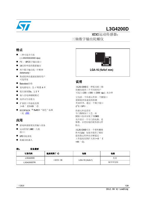
L3G4200D中文数据手册
3/24
图目录
L3G4200D
图目录
图1. 图2. 图3. 图4. 图5. 图6. 图7. 图8. 图9. 图10. 图11. 图12. 图13. 框图. . . . . . . . . . . . . . . . . . . . . . . . . . . . . . . . . . . . . . . . . . . . .5 引脚连接. . . . . . . . . . . . . . . . . . . . . . . . . . . . . . . . . . . . . . . . . . .5 L3G4200D外部低通滤波器值 SPI 从属 时序图(2). . . . . . . . . . . . . . . . . . . . . . . . . . . . . . . . . . . . . . 10 I2C 从属时序图(3) . . . . . . . . . . . . . . . . . . . . . . . . . . . . . . . . . . . . . .11 框图. . . . . . . . . . . . . . . . . . . . . . . . . . . . . . . . . . . . . . . . . . . . .14 读取和写入协议. . . . . . . . . . . . . . . . . . . . . . . . . . . . . . . . . . . . . . . .18 SPI阅读协议. . . . . . . . . . . . . . . . . . . . . . . . . . . . . . . . . . . . . . . . . 19 读取多个字节SPI协议(2字节的例子). . . . . . . . . . . . . . . . . . . . . . . . . . . . . . 19 SPI写协议. . . . . . . . . . . . . . . . . . . . . . . . . . . . . . . . . . . . . . . . . . 19 多个字节SPI字节写入协议(2例子). . . . . . . . . . . . . . . . . . . . . . . . . . . . . . . 20 SPI阅读3-wires模式协议. . . . . . . . . . . . . . . . . . . . . . . . . . . . . . . . . . . .20 LGA-16:机械数据和包装尺寸. . . . . . . . . . . . . . . . . . . . . . . . . . . . . . . . . . 22
- 1、下载文档前请自行甄别文档内容的完整性,平台不提供额外的编辑、内容补充、找答案等附加服务。
- 2、"仅部分预览"的文档,不可在线预览部分如存在完整性等问题,可反馈申请退款(可完整预览的文档不适用该条件!)。
- 3、如文档侵犯您的权益,请联系客服反馈,我们会尽快为您处理(人工客服工作时间:9:00-18:30)。
1/2
元器件交易网
Power Inductor & 2 in 1 Power Transformer < SMD Type: CLS Series>
Type: CLS4D23
◆ Specification
Part No.
Stamp
Inductance [Within]
2.4
1.1
CLS4D23NP -5R3N□ E 5.3µH±30% 1.5
1.1
0.72 0.60
2.0
0.85
CLS4D23NP -7R3N□ F 7.3µH±30% 1.3
1.1
0.54 0.45
1.8
0.75
CLS4D23NP -11ØN□ G
11µH±30% 0.9
0.70
0.47
0.41
元器件交易网
Power Inductor & 2 in 1 Power Transformer < SMD Type: CLS Series>
Type: CLS4D23
◆ Product Description
・5.2×5.0mm Max.(L×W), 2.5mm Max. Height. ・4 Terminal pins’ type gives a flexible design as inductors or transformers
Saturation Current(A) (at 20℃)※1
(1,4-2,3)
(2-3) (1,4 Short)
at20℃ at100℃ at20℃ at100℃
Temperature Rise current
(A) ※2
(1,4-2,3)
(2-3) (1,4 Short)
CLS4D23NP-1R2N□ A 1.2μH±30% 2.9
(SEPIC,ZETA circuit). ・Custom design is available.
◆ Feature
・Max. Operating frequency 1MHz, Max. ・2 in 1 Coils for high efficient up-down DC-DC converters (SEPIC, Zeta circuits to be used). ・Can be also used as DC-DC converter inductors. ・Ideally used in the power supply for DSC、Note PC、DVC and W-LED backlighting. ・RoHS Compliance
1.6
ቤተ መጻሕፍቲ ባይዱ0.62
CLS4D23NP -17ØN□ H
17µH±30% 0.72 0.65
0.40
0.30
1.1
0.45
CLS4D23NP -22ØN□ I
22µH±30% 0.57 0.55 0.27 0.22
1.1
0.43
※ Description Of Part Name
CLS4D23NP -1R2N□
2.5
1.5
1.3
4.0
1.8
CLS4D23NP -1R7N□ B 1.7µH±30% 2.6
2.2
1.3
1.0
3.2
1.4
CLS4D23NP -2R2N□ C 2.2µH±30% 2.4
1.9
1.1
0.9
3.0
1.3
CLS4D23NP -3R6N□ D 3.6µH±30% 1.7
1.4
1.0
0.75
◆ Dimensions (mm)
4.8±0.2
4.2
Max.2.5
2.6
5.0±0.2 2.1 4.85
Max.6.5
◆ Schematics (Bottom)
S2
3
◆ Land Pattern (mm)
3.1
1.5
1.0 1.8
1
4S
“ S” indicates winding start.
Please refer to the sales offices on our website for a representative near you
Please refer to the sales offices on our website for a representative near you
2/2
B Box C Carrier Tape
※1. Saturation Current: The DC current at which the inductance decreases to 90% of it’s nominal value.
※2.Temperature rise current: The DC current at which the temperature rise is △t=40℃.(Ta=20℃).