FYS-5012ABXX-XX中文资料
FOSAN富信电子 二级管 B5817WS-B5819WS-产品规格书
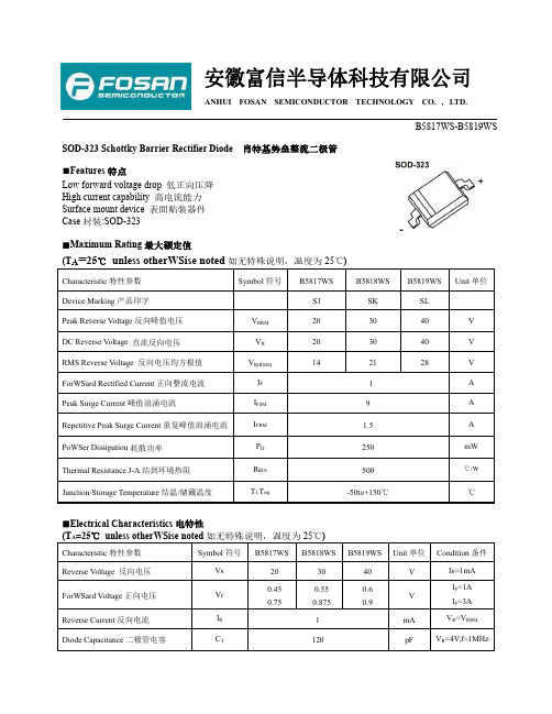
安徽富信半导体科技有限公司ANHUI FOSAN SEMICONDUCTOR TECHNOLOGY CO.,LTD.B5817WS-B5819WS SOD-323Schottky Barrier Rectifier Diode肖特基势垒整流二极管■Features特点Low forward voltage drop低正向压降High current capability高电流能力Surface mount device表面贴装器件Case封装:SOD-323■Maximum Rating最大额定值(T A=25℃unless otherWSise noted如无特殊说明,温度为25℃)Characteristic特性参数Symbol符号B5817WS B5818WS B5819WS Unit单位Device Marking产品印字SJ SK SLPeak Reverse Voltage反向峰值电压V RRM203040VDC Reverse Voltage直流反向电压V R203040V RMS Reverse Voltage反向电压均方根值V R(RMS)142128V ForWSard Rectified Current正向整流电流I F1A Peak Surge Current峰值浪涌电流I FSM9A Repetitive Peak Surge Current重复峰值浪涌电流I FRM 1.5A PoWSer Dissipation耗散功率P D250mW Thermal Resistance J-A结到环境热阻RθJA500℃/W Junction/Storage Temperature结温/储藏温度T J,T stg-50to+150℃℃■Electrical Characteristics电特性(T A=25℃unless otherWSise noted如无特殊说明,温度为25℃)Characteristic特性参数Symbol符号B5817WS B5818WS B5819WS Unit单位Condition条件Reverse Voltage反向电压V R203040V I R=1mAForWSard Voltage正向电压V F 0.450.750.550.8750.60.9VI F=1AI F=3AReverse Current反向电流I R1mA V R=V RRM Diode Capacitance二极管电容C T120pF V R=4V,f=1MHz安徽富信半导体科技有限公司ANHUI FOSAN SEMICONDUCTOR TECHNOLOGY CO.,LTD.B5817WS-B5819WS ■Typical Characteristic Curve典型特性曲线■Dimension外形封装尺寸SOD-323。
SWPA5012S100MT 绕线功率电感规格书
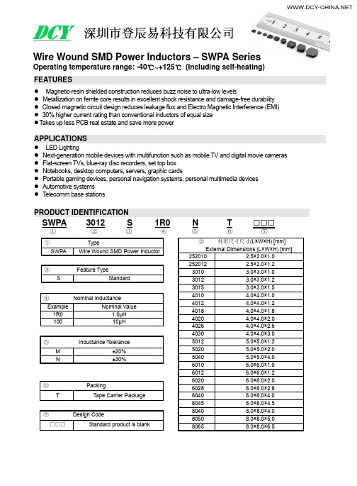
z LED Lighting z Next-generation mobile devices with multifunction such as mobile TV and digital movie cameras z Flat-screen TVs, blue-ray disc recorders, set top box z Notebooks, desktop computers, servers, graphic cards z Portable gaming devices, personal navigation systems, personal multimedia devices z Automotive systems z Telecomm base stations
4030
4.0×4.0×3.0
5012
5.0×5.0×1.2
5020
5.0×5.0×2.0
5040
5.0×5.0×4.0
6010
6.0×6.0×1.0
6012
6.0×6.0×1.2
6020
6.0×6.0×2.0
6028
6.0×6.0×2.8
6040
6.0×6.0×4.0
6045
6.0×6.0×4.5
A
B
C
D
E
F
a Typ. b Typ. c Typ.
SWPA252010S Fig.1 2.5±0.1 2.0±0.1 1.0 Max. 1.5±0.2 0.80±0.2 0.80±0.2 0.80 0.85 2.0
SWPA252012S Fig.1 2.5±0.1 2.0±0.1 1.2 Max. 1.5±0.2 0.80±0.2 0.80±0.2 0.80 0.85 2.0
R5013ANXFU6;中文规格书,Datasheet资料
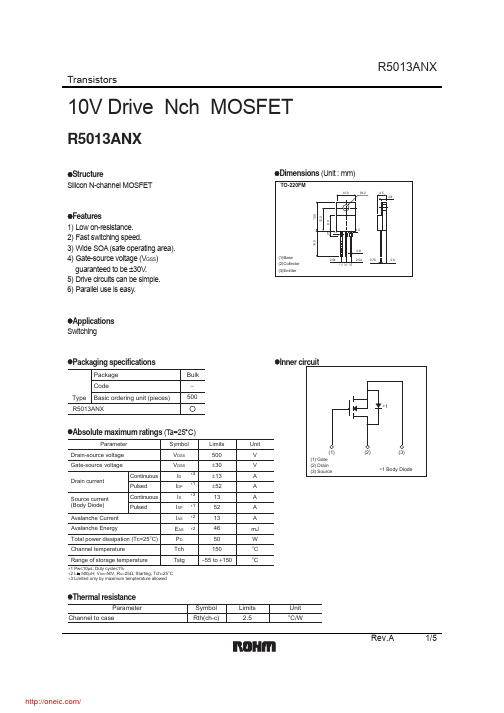
TransistorsRev.A 1/510V Drive Nch MOSFETR5013ANXz StructureSilicon N-channel MOSFETz Features1) Low on-resistance. 2) Fast switching speed.3) Wide SOA (safe operating area). 4) Gate-source voltage (V GSS ) guaranteed to be r 30V . 5) Drive circuits can be simple. 6) Parallel use is easy .z Applications Switchingz Dimensions (Unit : mm)z Packaging specificationszPackage CodeBasic ordering unit (pieces)−500Bulk R5013ANXTypez Absolute maximum ratings (T a=25q C)ParameterRange of storage temperatureChannel temperature Total power dissipation (Tc=25°C)Drain current Gate-source voltage Drain-source voltage V DSS V GSSP D Tch 500V V A W °C ±30±13I D I DP Continuous Pulsed A ±5250150Tstg°C−55 to +150Avalanche EnergyAvalanche Current I AS 13E AS 46Symbol Limits Unit ∗1 Pw ≤10μs, Duty cycle ≤1%∗2 L 500μH, V DD =50V, R G =25Ω, Starting, Tch =25°C ∗3 Limited only by maximum tempterature allowed∗1∗3∗3I S A I SP A A mJ Continuous Pulsed1352Source current (Body Diode)∗1∗2∗2z Thermal resistanceParameter°C/WRth(ch-c)Symbol Limits Unit Channel to case2.5TransistorsRev.A 2/5z Electrical characteristics (T a=25q C)z Body diode characteristics (Source-drain)(T a=25q C)V SD −− 1.5V I S = 13A, V GS =0VForward voltage∗ PulsedParameterSymbol Min.Typ.Max.Unit Conditions∗TransistorsRev.A 3/5z Electrical characteristic curves051015201020304050Fig.2: Typical Output Characteristics(㸇)0.0010.010.11101000.01.5 3.0 4.5 6.0Fig.4 Typical Transfer Characteristics0.010.11100.1110100Fig.6 Static Drain-Source On-StateResistance vs. Drain Current00.20.40.60.8151015Fig.7 Static Drain-Source On-State Resistance vs. Gate Source0.010.11101000.010.1110100Fig.9 Forward Transfer Admittance vs. Drain Current0.010.11101000.11101001000Fig.1 Maximum Safe Operating AeraFig.3: Typical Output Characteristics(㸈)246810012345Fig.8 Static Drain-Source On-State Resistance vs. Channel00.20.40.60.81-50050100150Fig.5 Gate Threshold Voltagevs. Channel0123456-50050100150DRAIN-SOURCE VOLTAGE : VDS ( V )D R A I N C U R R E N T : I D (A )DRAIN-SOURCE VOLTAGE: VDS (V)D R A I N C U R R E N T : I D (A )DRAIN-SOURCE VOLTAGE: V DS (V)D R A I N C U R R E N T : I D (A )DRAIN CURRENT : I D (A)S T A T I C D R A I N -S O U R C E O N -S T A T E R E S I S T A N C E : R D S (o n ) (ȍ)CHANNEL TEMPERATURE: T ch (°C)G A T E T H R E S H O L D V O L T A G E : V G S (t h ) (V )GATE-SOURCE VOLTAGE : V GS (V)D R A I N C U R R E N T : I D (A )GATE-SOURCE VOLTAGE : V GS (V)S T A T I C D R A I N -S O U R C E O N -S T A T E R E S I S T A N C E : R D S (o n ) (ȍ)CHANNEL TEMPERATURE: T ch (°C)DRAIN CURRENT : I D (A)F O R W A R D T R A N S F E R A D M I T T A N C E : |Y f s | (S )TransistorsRev.A 4/50.00010.0010.010.110.00010.0010.010.111010010001010010000.1110100Fig.13 Reverse Recovery Time vs.Reverse Drain Current0.010.11101000.511.5Fig.10 Reverse Drain Current vs. Sourse-Drain Voltage0510151020304050Fig.12 Dynamic Input Characteristics1101001000100000.010.11101001000Fig.11 Typical Capacitance vs. Drain-Source Voltage1101001000100000.010.1110100Fig.14 Switching 䇭CharacteristicsFig.15 Normalized Transient Thermal Resistance vs. Pulse WidthTOTAL GATE CHARGE : Q g (nC)G A T E -S O U R C E V O L T A G E : V G S (V )DRAIN-SOURCE VOLTAGE : V DS (V)C A P A C I T A N C E : C (p F )SOURCE-DRAIN VOLTAGE : V SD (V)R E V E R S E D R A I N C U R R E N T : I D R (A )REVERSE DRAIN CURRENT : I DR (A)R E V E R S E R E C O V E R Y T I M E : t r r (n s )DRAIN CURRENT : I D (A)S W I T C H I N G T I M E : t (n s )PULSE WIDTH : Pw(s)N O R M A R I Z E D T R A N S I E N T T H E R M A L R E S I S T A N C E : r (t )TransistorsRev.A 5/5z Switching characteristics measurement circuitFig.1 Switching time measurement circuit !Fig.2 Switching waveformsFig.3 Gate charge measurement circuit !Fig.4 Gate charge waveformFig.5 Avalanche measurement circuitFig.6 Avalanche waveformI G (Const.)Appendix1-Rev2.0Thank you for your accessing to ROHM product informations.More detail product informations and catalogs are available, please contact your nearest sales office.ROHM Customer Support SystemTHE AMERICAS / EUROPE / ASIA / JAPANContact us : webmaster@rohm.co.jpCopyright © 2008 ROHM CO.,LTD.21 Saiin Mizosaki-cho, Ukyo-ku, Kyoto 615-8585, JapanTEL : +81-75-311-2121FAX : +81-75-315-0172Appendix分销商库存信息: ROHMR5013ANXFU6。
恒电流二极管2DHMxxx、2DHLxxx系列产品
恒电流二极管2DHMxxx、2DHLxxx 系列产品恒电流二极管(CRD )是一种能为LED 或其他器件在电源电压变化时提供恒定电流的二端半导体器件, 它相当于一个大电流的恒流源或最大峰值电流限制电路,即使出现电源电压供应不稳定或是负载电阻变化很大的情况,都能确保供电电流恒定。
该器件具有外围电路非常简单、使用及其方便等特点,尤其适用于LED 照明、LCD 背光、汽车电子、通信电路、手持设备、仪器仪表和微型机器等场合。
■ 电气特性z 直流等效阻抗低; z 低电压启动; z 交流等效阻抗高; z 负温度系数;z 符合RoHS环保指令; Fig.1 恒电流二极管电路标示图 ■ 典型应用z LED驱动、LCD背光调节; z 手持设备、数码产品的恒流; z 通信设备、仪器仪表、微型机器; z 汽车电子;■ 产品系列、主要电气参数 (Ta=25℃,除非别有规定)参数测试标准:I H ---- 恒定电流值,测试条件:V V S 5=;V K ---- 起始恒流电压,测试条件:测试电流 H K I I 8.0=; Z D ---- 动态阻抗,测试条件:V V S 10=; V R ---- 反向耐压,测试条件:nA I R 50=;K C ---- 控制电流比,测试条件:H P C I I K /=; 时对应的电流是电压为E P V I ; T r ---- 脉冲上升时间; T f ---- 脉冲下降时间; I R ---- 反向漏电流 50nA;■产品系列、封装、最大额定值 :说明:1. 最大功耗P max 随型号、封装规格、散热条件会有所改变。
2. 工作温度范围:-30~+150 ℃3. 存储温度:-40~+150 ℃4. 焊接温度:260 ℃ 5.不带整流特性■ 测试电路Fig.2 恒电流二极管测试电路原理图 ■ 特性曲线Fig.3 恒电流二极管典型伏安特性曲线Fig.4 恒电流二极管典型温度特性曲线■ 典型应用电路Fig.5 单只恒电流二极管LED恒流电路Fig.6 多只恒电流二极管并联LED恒流电路* 对于直接用交流电输入的电路可在输入端的串联无极性分压电容(电容量的大小0.68μf/400v— 3.3μf/400v,视LED 的负载多少而定),由两个耐高压二极管(1N4007)和恒流二极管组成的双向恒流电路,直接驱动交流LED(双向LED)。
FOSAN富信电子 二级管 SD103AW-产品规格书

安徽富信半导体科技有限公司ANHUI FOSAN SEMICONDUCTOR TECHNOLOGY CO.,LTD.SD103AW SOD-123Schottky Barrier Rectifier Diode肖特基势垒整流二极管■Features特点Low forward voltage drop低正向压降High current capability高电流能力Surface mount device表面贴装器件Case封装:SOD-123Marking印字:S4■Maximum Rating最大额定值(T A=25℃unless otherwise noted如无特殊说明,温度为25℃)Characteristic特性参数Symbol符号Rating额定值Unit单位Peak Reverse Voltage反向峰值电压V RRM40VDC Reverse Voltage直流反向电压V R40V RMS Reverse Voltage反向电压均方根值V R(RMS)21V Forward Rectified Current正向整流电流I F0.35A Peak Surge Current峰值浪涌电流I FSM2A Power Dissipation耗散功率P D310mW Thermal Resistance J-A结到环境热阻RθJA400℃/W Junction/Storage Temperature结温/储藏温度T J,T stg-50to+150℃℃■Electrical Characteristics电特性(T A=25℃unless otherwise noted如无特殊说明,温度为25℃)Characteristic 特性参数Symbol符号Min最小值Type典型值Max最大值Unit单位Condition条件Reverse Voltage反向电压V R40V I R=1mA Forward Voltage正向电压V F0.6V I F=0.2AReverse Current反向电流I R 0.058mAV R=40V(25℃)(100℃)Diode Capacitance二极管电容C T20pF V R=4V,f=1MHzANHUI FOSAN SEMICONDUCTOR TECHNOLOGY CO.,LTD.SD103AW ■Typical Characteristic Curve典型特性曲线ANHUI FOSAN SEMICONDUCTOR TECHNOLOGY CO.,LTD.SD103AW ■Dimension外形封装尺寸。
T8XX-XXXH中文资料

®1/11Table 1: Main FeaturesDESCRIPTIONAvailable either in through-hole or surface-mount packages, the BTA08, BTB08 and T8 triac series is suitable for general purpose AC switching. They can be used as an ON/OFF function in applica-tions such as static relays, heating regulation, in-duction motor starting circuits... or for phase control operation in light dimmers, motor speed controllers,...The snubberless versions (BTA/BTB...W and T8series) are specially recommended for use on inductive loads, thanks to their high commutation performances.Logic level versions are designed to interface directly with low power drivers such as microcontrollers.By using an internal ceramic pad, the BTA series provides voltage insulated tab (rated at 2500V RMS ) complying with UL standards (file ref.:E81734).Symbol Value Unit I T(RMS)8A V DRM /V RRM 600 and 800V I GT (Q 1)5 to 50mABTA08, BTB08 and T8 Series8A TRIAC SREV. 6February 2006SNUBBERLESS™, LOGIC LEVEL & STANDARDTable 2: Order CodesPart Number Marking BTA08-xxxxxRG See page table 8 onpage 10BTB08-xxxxxRG T8xx-xxxG T8xx-xxxH T8xx-xxxBBTA08, BTB08 and T8 Series2/11Table 3: Absolute Maximum Ratings Tables 4: Electrical Characteristics (T j = 25°C, unless otherwise specified)■SNUBBERLESS and Logic Level (3 quadrants)Symbol ParameterValue Unit I T(RMS)RMS on-state current (full sine wave)IPAK/D 2PAK/DPAK/TO-220AB T c = 110°C 8ATO-220AB Ins.T c = 100°C I TSM Non repetitive surge peak on-state current (full cycle, T j initial = 25°C) F = 50 Hz t = 20 ms 80A F = 60 Hz t = 16.7 ms84I ²t I ²t Value for fusingt p = 10 ms 36A ²s dI/dt Critical rate of rise of on-state cur-rent I G = 2 x I GT , t r ≤ 100 ns F = 120 Hz T j = 125°C 50A/µs I GM Peak gate currentt p = 20 µsT j = 125°C 4A P G(AV)Average gate power dissipation T j = 125°C1W T stg T jStorage junction temperature rangeOperating junction temperature range- 40 to + 150- 40 to + 125°CSymbol Test ConditionsQuad-rantT8BTA08 / BTB08Unit T810T835TW SW CW BW I GT (1)V D = 12 V R L = 30 ΩI - II -III MAX.10355103550mA V GT I - II - III MAX.1.3V V GD V D = V DRM R L = 3.3 k ΩT j = 125°C I - II - IIIMIN.0.2V I H (2)I T = 100 mA MAX.153510153550mA I L I G = 1.2 I GTI - III MAX.255010255070mAII306015306080dV/dt (2)V D = 67 %V DRM gate open T j = 125°CMIN.4040020404001000V/µs (dI/dt)c (2)(dV/dt)c = 0.1 V/µs T j = 125°CMIN.5.4- 3.5 5.4--A/ms(dV/dt)c = 10 V/µs T j = 125°C2.8- 1.5 2.98--Without snubber T j = 125°C- 4.5-- 4.57BTA08, BTB08 and T8 Series3/11■Standard (4 quadrants)Table 5: Static Characteristics Table 6: Thermal resistance Symbol Test ConditionsQuadrant BTA08 / BTB08Unit C B I GT (1)V D = 12 V R L = 30 ΩI - II - III IV MAX.255050100mA V GT ALL MAX. 1.3V V GD V D = V DRM R L = 3.3 k Ω T j = 125°C ALLMIN.0.2V I H (2)I T = 500 mA MAX.2550mA I L I G = 1.2 I GTI - III - IVMAX.4050mA II80100dV/dt (2)V D = 67 %V DRM gate open T j = 125°CMIN.200400V/µs (dV/dt)c (2)(dI/dt)c = 5.3 A/ms T j = 125°C MIN.510V/µsSymbol Test ConditionsValueUnit V T (2)I TM = 11 A t p = 380 µs T j = 25°C MAX. 1.55V V to (2)Threshold voltage T j = 125°C MAX.0.85V R d (2)Dynamic resistance T j = 125°C MAX.50m ΩI DRM I RRMV DRM = V RRMT j = 25°C MAX.5µA T j = 125°C1mANote 1: minimum I GT is guaranted at 5% of I GT max.Note 2: for both polarities of A2 referenced to A1.Symbol ParameterValue Unit R th(j-c)Junction to case (AC)IPAK / D 2PAK / DPAK / TO-220AB 1.6°C/WTO-220AB Insulated 2.5R th(j-a)Junction to ambientS = 1 cm ²D 2PAK 45°C/WS = 0.5 cm ²DPAK70TO-220AB / TO-220AB Insulated 60IPAK100S = Copper surface under tab.BTA08, BTB08 and T8 Series4/11Figure 1: Maximum power dissipation versus RMS on-state current (full cycle)Figure 2: RMS on-state current versus case temperature (full cycle)Figure 3: RMS on-state current versus ambient temperature (printed circuit board FR4, copper thickness: 35µm) (full cycle)Figure 4: Relative variation of thermal impedance versus pulse durationFigure 5: On-state characteristics (maximum values)Figure 6: Surge peak on-state current versus number of cyclesBTA08, BTB08 and T8 Series5/11Figure 7: Non-repetitive surge peak on-state current for a sinusoidal pulse with width t p < 10 ms and corresponding value of I 2tFigure 8: Relative variation of gate trigger current, holding current and latching current versus junction temperature (typical values)Figure 9: Relative variation of critical rate of decrease of main current versus (dV/dt)c (typical values) (Snubberless & L ogic level types)Figure 10: Relative variation of critical rate of decrease of main current versus (dV/dt)c (typical values) (Standard types)Figure 11: Relative variation of critical rate of decrease of main current versus junction temperatureFigure 12: DPAK and D 2P AK Thermal resistance junction to ambient versus copper surface under tab (printed circuit board FR4, copper thickness:35µm)BTA08, BTB08 and T8 Series6/11Figure 13: Ordering Information Scheme (BTA08 and BTB08 series)Figure 14: Ordering Information Scheme (T8 series)Table 7: Product SelectorPart NumberVoltage (xxx)Sensitivity Type Package 600 V 800 V BTA/BTB08-xxxB X X 50 mA Standard TO-220AB BTA/BTB08-xxxBW X X 50 mA Snubberless TO-220AB BTA/BTB08-xxxC X X 25 mAStandard TO-220AB BTA/BTB08-xxxCW X X 35 mA Snubberless TO-220AB BTA/BTB08-xxxSW X X 10 mA Logic level TO-220AB BTA/BTB08-xxxTW X X 5 mA Logic Level TO-220AB T810-xxxG X X 10 mA Logic Level D2PAK T810-xxxH X X 10 mA Logic Level IPAK T835-xxxB X X 35 mA Snubberless DPAK T835-xxxG X X 35 mA Snubberless D 2PAK T835-xxxHXX35 mASnubberlessIPAKBTB: non insulated TO-220AB packageBTA08, BTB08 and T8 Series Figure 15: D2PAK Package Mechanical DataFigure 16: D2PAK Foot Print Dimensions(in millimeters)7/11BTA08, BTB08 and T8 SeriesFigure 17: DPAK Package Mechanical DataFigure 18: DPAK Foot Print Dimensions (in millimeters)8/11BTA08, BTB08 and T8 Series9/11BTA08, BTB08 and T8 Series10/11In order to meet environmental requirements, ST offers these devices in ECOPACK® packages. These packages have a Lead-free second level interconnect . The category of second level interconnect is marked on the package and on the inner box label, in compliance with JEDEC Standard JESD97. The maximum ratings related to soldering conditions are also marked on the inner box label. ECOPACK is an ST trademark. ECOPACK specifications are available at: .Table 8: Ordering InformationOrdering type Marking Package Weight Base qtyDelivery modeBTA/BTB08-xxxyzRGBTA/BTB08-xxxyzTO-220AB 2.3 g 50Tube T8yy-xxxG T8yyxx D 2PAK 1.5 g 50Tube T8yy-xxxG-TR T8yyxx 1000Tape & reel T8yy-xxxB T8yyxx DPAK 0.3 g 75Tube T8yy-xxxB-TR T8yyxx 2500Tape & reel T8yy-xxxHT8yyxxIPAK0.4 g75TubeNote: xxx = voltage, yy = sensitivity, z = typeTable 9: Revision HistoryDate Revision Description of ChangesApr-20025A Last update.13-Feb-20066TO-220AB delivery mode changed from bulk to tube.ECOPACK statement added.元器件交易网BTA08, BTB08 and T8 Series Information furnished is believed to be accurate and reliable. However, STMicroelectronics assumes no responsibility for the consequencesof use of such information nor for any infringement of patents or other rights of third parties which may result from its use. No license is grantedby implication or otherwise under any patent or patent rights of STMicroelectronics. Specifications mentioned in this publication are subjectto change without notice. This publication supersedes and replaces all information previously supplied. STMicroelectronics products are notauthorized for use as critical components in life support devices or systems without express written approval of STMicroelectronics.The ST logo is a registered trademark of STMicroelectronics.All other names are the property of their respective owners© 2006 STMicroelectronics - All rights reservedSTMicroelectronics group of companiesAustralia - Belgium - Brazil - Canada - China - Czech Republic - Finland - France - Germany - Hong Kong - India - Israel - Italy - Japan - Malaysia - Malta - Morocco - Singapore - Spain - Sweden - Switzerland - United Kingdom - United States of America11/11。
FOSAN富信电子 二级管 LL4148-产品规格书
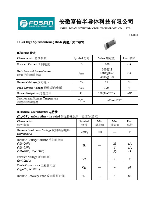
安徽富信半导体科技有限公司ANHUI FOSAN SEMICONDUCTOR TECHNOLOGY CO.,LTD.LL4148LL-34High Speed Switching Diode 高速开关二极管▉Features 特点Characteristic 特性参数Symbol 符号Value 额定值Unit 单位Forward Current 正向电流I F 200mA Peak Forward Surge Current 峰值正向浪涌电流I FSM 500@1S 1000@1mS 4000@1µSmA Reverse Voltage 反向电压V R 75V Peak Reverse V oltage 峰值反向电压V RM 100V Power dissipation 耗散功率P D 500(Ta=25℃)mWJunction and Storage Temperature 结温和储藏温度T J ,T stg-65to+175℃■Electrical Characteristics 电特性(TA =25℃unless otherwise noted 如无特殊说明,温度为25℃)Characteristic 特性参数Symbol 符号Min 最小值Max 最大值Unit 单位Reverse Breakdown Voltage 反向击穿电压(I R =100uA)V (BR)100—VReverse Leakage Current 反向漏电流(V R =20V)(V R =75V)(V R =20V ,T J =150℃)I R —25550nA µA µA Forward V oltage 正向电压(I F =10mA)V F —1V Diode Capacitance 二极管电容(V R =0V,f=1MHz)C D—4pF Reverse Recovery Time 反向恢复时间T rr—4nSANHUI FOSAN SEMICONDUCTOR TECHNOLOGY CO.,LTD.LL4148■Typical Characteristic Curve典型特性曲线Figure1:Forward Characteristics Figure2:Leakage CurrentFigure3:Capacitance Characteristics Figure4:Power Derating CurveANHUI FOSAN SEMICONDUCTOR TECHNOLOGY CO.,LTD.LL4148■Dimension外形封装尺寸。
双壁波纹管产品完整规格型号及产品对应生产执行标准

米
T/CECS 10011-2019
20 给排水材料 管材
21 给排水材料 管材
22 给排水材料 管材
23 给排水材料 管材
24 给排水材料 管材
25 给排水材料 管材
26 给排水材料 管材
27 给排水材料 管材
28 给排水材料 管材
29 给排水材料 30 给排水材料
管材 管材
塑料管 塑料管 塑料管 塑料管 塑料管 塑料管 塑料管 塑料管 塑料管 塑料管 塑料管
高分子量高密度聚乙 烯(HMWHDPE)双 DN200 SN8 壁波纹管 高分子量高密度聚乙 烯(HMWHDPE)双 DN300 SN8 壁波纹管 高分子量高密度聚乙 烯(HMWHDPE)双 DN400 SN8 壁波纹管 高分子量高密度聚乙 烯(HMWHDPE)双 DN500 SN8 壁波纹管 高分子量高密度聚乙 烯(HMWHDPE)双 DN600 SN8 壁波纹管 埋地排水用聚乙烯共 混聚氯乙烯双壁波纹 ID 200 SN8 管材 埋地排水用聚乙烯共 混聚氯乙烯双壁波纹 ID 300 SN8 管材 埋地排水用聚乙烯共 混聚氯乙烯双壁波纹 ID 400 SN8 管材 埋地排水用聚乙烯共 混聚氯乙烯双壁波纹 ID 500 SN8 管材
管材
管材
管材
管材
管材
管材
管材
管材
管材
管材
管材
管材 管材 管材 管材 管材 管材 管材
塑料管
塑料管
塑料管
塑料管
塑料管
塑料管
塑料管
塑料管
塑料管
塑料管
塑料管
塑料管 塑料管 塑料管 塑料管 塑料管 塑料管 塑料管
增强聚丙烯FRPP双壁 加筋波纹管
- 1、下载文档前请自行甄别文档内容的完整性,平台不提供额外的编辑、内容补充、找答案等附加服务。
- 2、"仅部分预览"的文档,不可在线预览部分如存在完整性等问题,可反馈申请退款(可完整预览的文档不适用该条件!)。
- 3、如文档侵犯您的权益,请联系客服反馈,我们会尽快为您处理(人工客服工作时间:9:00-18:30)。
PartNO.:FYS-5012A/BXX-XX
ADD:NO.115QiXin Road NingBo Zhejiang China ZIP.:315051DESCRIPTION
●
12.70mm (0.5”)Single digit numeric display series.
●
Standard brightness.●Low current operation.
●Excellent character apperance.
●Easy mounting on P.C.boards or sockets
Package Dimensions &Internal Circuit Diagram
Notes:
·
All dimensions are in millimeters (inches)
·Tolerance is ±
0.25(0.01")unless
otherwise noted.
·Specificaions are subject to change whitout notice.
PartNO.:FYS-5012A/BXX-XX
ADD:NO.115QiXin Road NingBo Zhejiang China ZIP.:315051:Absolute maximum ratings (Ta=25℃)
Value
Parameter Symbol Test Condition
Min
Max
Unit
Reverse V oltage VR IR=30μA 5-----V Forward
Current
IF -----------30mA Power Dissipation Pd -----------100mW Pulse Current Ipeak Duty=0.1mS,1KHz ------150mA Operating Temperature Topr ------40+85°C Storage Temperature
Tstr
-----
-40
+85
°C
■Description:
·Color Code &Chip characteristics:(Test Condition:IF=20mA)
Forward Voltage(VF)Unit:V Emitting Color Dice Material Peak
Wave
Length (λP )Spectral Line halfwidth(△
λ1/2)Typ Max Luminous Intensity (Iv)Unit:ucd H
Red GaP/GaP
700nm 90nm 2.25 2.50500S Hi Red GaAlAs/GaAs,SH 660nm 20nm 1.85 2.203500D Super Red GaAlAs/GaAs,DH 660nm 20nm 1.85 2.206000UR Ultra Red GaAlAs/GaAs,DD H
660nm 20nm 1.85 2.2012000E Orange GaAsP/GaP 635nm 35nm 2.10 2.502500Y Yellow GaAsP/GaP 585nm 35nm 2.10 2.502000G
Green
GaP/GaP
570nm
30nm
2.20
2.50
2500
·-XX:Surface /Lens color :
Number
1
2
3
4
5
Ref Surface Color White Black Gray Red Green Epoxy Color
Water clear
White diffused
Red Diffused
Green Diffused
Yellow Diffused
PartNO.:FYS-5012A/BXX-XX
ADD:NO.115QiXin Road NingBo Zhejiang China ZIP.:3150511.0
0.5
350
4004505005506006507007508008509009501000
(A)
(B)
(C)
(D)
(2)
(3)
(8)
(4)
(1)(6)
(5)
(9)
(10)
Wavelength(nm)
RELATIVE INTENSITY Vs WAVELENGTH()
λp (1)-GaAsP/GaAs 655nm/Red (2)-GaP 570nm/Yellow Green (3)-GaAsP/GaP 585nm/Yellow
(4)-GaAsp/GaP 635nm/Orange &Hi-Eff Red (5)-GaP 700nm/Bright Red
(6)-GaAlAs/GaAs 660nm/Super Red (8)-GaAsP/GaP 610nm/Super Red
(9)-GaAlAs 880nm
(10)-GaAs/GaAs &GaAlAs/GaAs 940nm (A)-GaN/SiC 430nm/Blue (B)-InGaN/SiC 470nm/Blue
(C)-(D)-InGaN/SiC 505nm/Ultra Green InGaAl/SiC 525nm/Ultra Green
504030201001.2
1.6
2.0 2.4 2.6
3.0
1
63
45
28
50403020100
20406080100
16
2,4,8,A 35
3210.50.20.1-30
-20
-10
10
20
30
40
50
60
70
15423
1098765432
1
1
10100100010,00010KHz 3KHz
1KHz 300KHz 100KHz F-REFRESH RATE
100KHz 30KHz
10KHz 3KHz 1KHz 300Hz 100Hz 1098765
4321
1
10100100010,000
FORWARD VOLT AGE (Vf)FORWARD CURRENT VS.FORWARD VOLTAGE
RELATIVE LUMINOUS
INTENSITY VS.FORWARD CURRENT
AMBIENT TEMPERATURE T a()℃FORWARD CURRENT VS.AMBIENT TEMPERATURE
tp-PULSE DURATION uS (1,2,3,4,6,8,B.D.J.K)
NOTE:25free air temperature unless otherwise specified
℃tp-PULSE DURATION uS
FORWARD CURRENT(mA)FORWARD CURRENT (mA)RELA TIVE LUMINOUS INTENSITY
FORWARD CURRENT(mA)
RELATIVE LUMINOUS INTENSITY
AMBIENT TEMPERATURE T a()
℃(5)
Ipeak MAX.IDC MAX.
Ipeak MAX.IDC MAX.
PartNO.:FYS-5012A/BXX-XX
ADD:NO.115QiXin Road NingBo Zhejiang China ZIP.:315051
tapy QTY/foam(pcs)QTY /Bundle (pcs)QTY /CARTONDimension。