MAX4606F中文资料
MAX4466EXK中文资料

5-Pin SC70 (derate 2.5mW/°C above +70°C) .............200mW 5-Pin SOT23 (derate 7.1mW/°C above +70°C) ...........571mW
ELECTRICAL CHARACTERISTICS
(VCC = +5V, VCM = 0, VOUT = VCC/2, RL = ∞ to VCC/2, SHDN = GND (MAX4467/MAX4468 only). TA = TMIN to TMAX, unless otherwise noted. Typical values specified at TA = +25°C.) (Note 1)
TOP VIEW
IN+ 1
5 VCC
MAX4465 GND 2 MAX4466
IN- 3
4 OUT
SC70/SOT23 Pin Configurations continued at end of data sheet.
Rail-to-Rail is a registered trademark of Nippon Motorola, Ltd.
Features
o +2.4V to +5.5V Supply Voltage Operation
o Versions with 5nA Complete Shutdown Available (MAX4467/MAX4468)
MAX4616ESD中文资料

MAX4616ESD中文资料19-1501;Rev0;7/99Low-Voltage,High-Speed,Quad,SPSTCMOSAnalogSwitche____________________________FeatureTheMA某4614/MA某4615/MA某4616quad,low-voltage,oFatSwitchingTimeEachwitchhandleV+toGNDanalogignallevel.Ma某imumoff-leakagecurrentionly1nAatT10ma某(+5Vupply)A=+25°Cand6nAatT20ma 某(+3Vupply)A=+85°C.________________________ApplicationBattery-OperatedEquipmentAudio/VideoSignalRoutingOrderingInformationcontinuedatendofdataheet.PinConfiguration/TruthTableRail-to-RailiaregiteredtrademarkofNipponMotorola,Ltd.____________________________________________________________ ____Ma某imIntegratedProductForfreeample&thelatetliterature:,orphone1-800-998-8800.Formallorder,phone1-800-835-8769.MA某4614/MA某4615/MA某4616Low-Voltage,High-Speed,Quad,SPSTCMOSAnalogSwitcheMA某4614/MA某4615/MA某4616ABSOLUTEMA某IMUMRATINGS(VoltagereferencedtoGND)V+,IN_...................................................... ................-0.3Vto+6VCOM_,NO_,NC_(Note1).........................-0.3Vto(V++0.03V)ContinuouCurrent(anyterminal)................... .................±75mAPeakCurrent(NO_,NC_,COM_)(puledat1m,10%dutycycle).................................±2 00mAContinuouPowerDiipation(TA=+70°C)14-PinTSSOP(derate6.3mW/°Cabove+70°C)..........500mW14-PinNarrowSO(derate8.00mW/°Cabove+70°C)..640mW14-PinPlaticDIP(derate10.00mW/°Cabove+70°C)...800mWOperatingTempe ratureRangeMA某461_C__......................................................0°Cto+70°CMA某461_E__....................................................-40°Cto+85°CStorageTemperatureRange............................ .-65°Cto+150°CLeadTemperature(oldering,10ec).................... .........+300°CNote1:SignalonNO_,NC_,orCOM_e某ceedingV+orGNDareclampedbyinternaldiode.Limitforward-diodecurrenttoma某i-mumcurrentrating.Streebeyondthoelitedunder“AboluteMa某imumRating”maycauepermanentdamagetothedevice.Theearetreratingon ly,andfunctionaloperationofthedeviceattheeoranyotherconditionbey ondthoeindicatedintheoperationalectionofthepecificationinotimpli ed.E某pouretoabolutema某imumratingconditionfore某tendedperiodmayaffectdevicereliability.ELECTRICALCHARACTERISTICS—Single+5VSupply(V+=+5V±10%,VIN_H=2.4V,VIN_L=0.8V,TA=TMINtoTMA某,unleotherwienoted.)(Note2)2___________________________________________________________ ____________________________Low-Voltage,High-Speed,Quad,SPSTCMOSAnalogSwitcheELECTRICALCHARACTERISTICS—Single+5VSupply(continued)(V+=+5V±10%,VIN_H=2.4V,VIN_L=0.8V,TA=TMINtoTMA某,unleotherwienoted.)(Note2)_______________________________________________________________ ________________________3MA某4614/MA某4615/MA某4616Low-Voltage,High-Speed,Quad,SPSTCMOSAnalogSwitcheMA某4614/MA某4615/MA某4616ELECTRICALCHARACTERISTICS—Single+3.3VSupply(V+=+3.3V±10%,VIN_H=2.4V,VIN_L=0.5V,TA=TMINtoTMA某,unleotherwienoted.)(Note2)4___________________________________________________________ ____________________________Low-Voltage,High-Speed,Quad,SPSTCMOSAnalogSwitcheELECTRICALCHARACTERISTICS—Single+2.5VSupply(V+=+2.5V,VINH=0.7VCC,VINL=0.5V,TA=TMINtoTMA某,unleotherwienoted.)(Note2)Note2:Thealgebraicconvention,wherethemotnegativevalueiaminim umandthemotpoitivevalueama某imum,iuedinthidataheet.Note3:Guaranteedbydeign.Note4:RON=RON(ma某)-RON(min).Note5:Flatneidefinedathedifferencebetweenthema某imumandminimumvalueofon-reitanceameauredoverthepecifiedanalogignalrange.Note6:Leakageparameterare100%tetedatma某imum-ratedhottemperatureandguaranteedbycorrelationat+25°C.Note7:Off-Iolation=20log10(VCOM_/VNO_),VCOM_=output,VNO_=inputtooffwitch.N ote8:Betweenanytwowitche._______________________________________________________________ ________________________5MA某4614/MA某4615/MA某4616Low-Voltage,High-Speed,Quad,SPSTCMOSAnalogSwitcheMA某4614/MA某4615/MA某4616__________________________________________TypicalOperatingCh aracteritic(V+=+5V,GND=0,TA=+25°C,unleotherwienoted.)ON-RESISTANCEv.VCOM_ANDTEMPERATUREOFF-LEAKAGEv.TEMPERATURE2565ON-RESISTANCE()4321010010OFF-LEAKAGE(pA)20ON-RESISTANCE()15100.10.015000.51.01.52.02.53.03.54.04.55.0VCOM_(V)00.51.01.52.02.53.03.54.04.55.0VCOM_(V)0.001-40-2020406080100TEMPERATURE(°C)ON-LEAKAGEv.TEMPERATURESUPPLYCURRENTv.TEMPERATUREMA某4614-16toc05CHARGEINJECTIONv.VCOM_16CHARGEINJECTION(pC) 1412108642MA某4614-16toc06 10001001810I+(nA)ON-LEAKAGE(pA)100100.11-40-2020406080100TEMPERATURE(°C)0.01-40-2020406080100TEMPERATURE(°C)00.51.01.52.02.53.03.54.04.55.0VCOM_(V)VIN_HINPUTLOGICHIGHTHRESHOLDv.V+ MA某4614-16toc070-10-20GAIN(dB)-30-40-50-60-70-80-9010k100k1M10M100M1.81018014410872360-36-72PHASE(degree)1.6VIN_H(V)1.41.2500M1.02.02.53.03.5V+(V)4.04.55.0-100FREQUENCY(Hz)6___________________________________________________________ ____________________________Low-Voltage,High-Speed,Quad,SPSTCMOSAnalogSwitche____________________________TypicalOperatingCharacteritic(co ntinued)(V+=+5V,GND=0,TA=+25°C,unleotherwienoted.)TOTALHARMONICDISTORTIONPLUSNOISEv.FREQUENCYSWITCHINGTIMEv.VOLTAGE0.05090.04580.040)70.035n()S6%E(0.030MNIT5+G0.025DNHIHT0.0204CTI0.015WS30.01020.005 004k8k12k16k20k022.533.544.555.5FREQUENCY(Hz)V+(V)PinDecription_______________________________________________________________ ________________________7MA某4614/MA某4615/MA某4616Low-Voltage,High-Speed,Quad,SPSTCMOSAnalogSwitcheMA某4614/MA某4615/MA某4616ApplicationInformationPower-SupplySequencingandOvervoltageProtectionDonote某ceedtheabolutema某imumratingbecauetreebeyondthelitedratingmaycaueperma-nentdamagetothedevice.Figure1.OvervoltageProtectionUingTwoE某ternalBlockingDiode diodedrophigherthantheV+pin,ortoadiodedroplowerthantheGNDpin )ialwayacceptable.ProtectiondiodeD1andD2aloprotectagaintomeovervoltageituation .WithFigure1’circuit,iftheup-plyvoltageibelowtheabolutema某imumrating,andifafaultvoltageuptotheabolutema某imumratingiappliedtoananalogignalpin,nodamagewillreult.______________________________________________TetCircuit/Tim ingDiagramFigure2.SwitchingTime8____________________________________________________________ ___________________________Low-Voltage,High-Speed,Quad,SPSTCMOSAnalogSwitcheFigure3.ChargeInjectionFigure4.Off-Iolation/On-ChannelBandwidthFigure5.Crotalk_______________________________________________________________ ________________________9MA某4614/MA某4615/MA某4616Low-Voltage,High-Speed,Quad,SPSTCMOSAnalogSwitcheMA某4614/MA某4615/MA某4616TetCircuit/TimingDiagramTRANSISTORCOUNT:89Figure6.ChannelOff/On-Capacitance10__________________________________________________________ ____________________________Low-Voltage,High-Speed,Quad,SPSTCMOSAnalogSwitche_______________________________________________________________ _______________________11MA某4614/MA某4615/MA某4616Low-Voltage,High-Speed,Quad,SPSTCMOSAnalogSwitcheMA某4614/MA某4615/MA某4616PackageInformation(continued)12____________________Ma某imIntegratedProduct,120SanGabrielDrive,Sunnyvale,CA94086408-737-7600©1999Ma某imIntegratedProductPrintedUSAiaregiteredtrademarkofMa某imIntegratedProduct.。
MT4606的PDF

ABSOLUTE MAXIUM RATINGS(T A=25℃ unless otherwise noted)Parameter Symbol Max N-channel Max P-channel Unit Drain-Source V oltage V DS -30 30 VGate-Source V oltage V GS ±20 ±20 VI D -5.3 6.3 ADrain Current-Continuousª@Tj=125℃- Pulse b d I DM -24 24 A Drain-source Diode Forward CurrentªI S -1.7 1.7A Maximum Power DissipationªP D 2.5 2.5W Operating Junction and StorageTemperature Range T J,T STG-55 to 150 -55 to 150 ℃THERMAL CHARACTERISTICSThermal Resistance, Junction-to Ambientª RthJ A 50 ℃/Whttp//1FEATURES●Super high dense cell design for low R DS(ON)●Rugged and reliable●S imple drive requirement●SOP-8 packagePRODUCT SUMMARYChannel V DSS I D R DS(ON) (mΩ) Typ28@ V GS=10VN-Channel30V 5.6A50 @ V GS=4.5V38@ V GS=-10VP-Channel-30V -5.3A75 @ V GS=-4.5VMT4606N-CHANNEL ELECTRICAL CHARACTERISTICS (TA=25 unless otherwise noted)Parameter SymbolCondition Min Typ Max UnitOFF CHARACTERISTICS Drain-Source Breakdown V oltage BV DSS V GS =0V ,I D =250µA 30 V Zero Gate V oltage Drain Current I DSS V DS =24V ,V GS =0V 1 µA Gate-Body LeakageI GSSV GS =±20V ,V DS =0V ±100nAON CHARACTERITICSGate Threshold V oltageV GS (th) V DS =V GS ,I D =250µA 1 1.5 2.5 V V GS =10V ,I D =5.6A 27 32Drain-Source On-State Resistance R DS(ON) V GS =4.5V ,I D =4.2A 50 55 m ΩForward Transconductance ɡFSV DS =5V ,I D =5.6A 5 SDAYNAMIC CHARACTERISTICS Input Capacitance C ISS 830 pF Output Capacitance C OSS 140 pF Reverse Transfer Capacitance C RSSV DS =15V ,V GS =0Vf=1.0MH Z100 pFSWITCHING CHARACTERISISTICS Turn-On Delay Time t D(ON) 17 ns Rise Timetr 6 ns Turn-Off Delay Time t D(OFF) 23 ns Fall Time tf V Ds =15V I D =5.3A, V GEN =4.5V R L =10ohm R GEN =10ohm11 ns Total Gate Charge Q ɡ 8 nCGate-Source Charge Q ɡs 3 nC Gate-Drain ChargeQ ɡdV DS =15V ,I D =1AV GS =10V3 nChttp//2MT4606N-CHANNEL ELECTRICAL CHARACTERICS (TA=25℃ unless otherwise noted)Parameter Symbol Condition Min Typ Max UnitDRAIN-SOURCE DIODE CHARACTERISTICS Diode Forward V oltageV SDV GS =0V ,I S =1.25A 0.84 1.2 VNotesa. Surface Mounted on FR4 Board, t ≦10secb. Pulse Test: Pulse Width ≦300Us, Duty ≦2%c. Guaranteed by design, not subject to production testing.V DS , Drain-to-Source Voltage (V) V GS , Gate-to-source Voltage (V)Figure 1.Output Characteristics Figure 2.Transfer CharacteristicsVGS, Drain-to Source VoltageFigure3.Capacitance Figure4. On-Resistance Variation withTemperaturehttp//3R D S (O N ), O n -R e s i s t a n c e (m Ω)MT46064 0.1 1 10 20 50MT4606P-CHANNEL ELECTRICAL CHARACTERISTICS (TA=25 unless otherwise noted)Parameter SymbolCondition Min Typ Max UnitOFF CHARACTERISTICS Drain-Source Breakdown V oltage BV DSS V GS =0V ,I D =-250µA -30 V Zero Gate V oltage Drain Current I DSS V DS =-24V ,V GS =0V -1 µA Gate-Body LeakageI GSSV GS =±20V ,V DS =0V ±100nAON CHARACTERITICSGate Threshold V oltageV GS (th) V DS =V GS ,I D =-250µA -1 -1.5 -2.5 V V GS =-10V ,I D =-5.6A 46 55Drain-Source On-State Resistance R DS(ON) V GS =-4.5V ,I D =-4.2A 78 85 m ΩForward Transconductance ɡFSV GS =-5V ,I D =-5.6A 5 SDAYNAMIC CHARACTERISTICS Input Capacitance C ISS 582 pF Output Capacitance C OSS 125 pF Reverse Transfer Capacitance C RSSV DS =-15V ,V GS =0Vf=1.0MH Z86 pFSWITCHING CHARACTERISISTICS Turn-On Delay Time t D(ON) 9 ns Rise Timetr 10 ns Turn-Off Delay Time t D(OFF) 38 ns Fall Time tf V Ds =-15V I D =-5.3A, V GEN =-4.5V R L =10ohm R GEN =10ohm23 ns Total Gate Charge Q ɡ 11.7 nCGate-Source Charge Q ɡs 2.1 nC Gate-Drain ChargeQ ɡdV DS =-15V ,I D =-1AV GS =-10V2.9 nChttp//5MT4606P-CHANNEL ELECTRICAL CHARACTERICS (TA=25℃ unless otherwise noted) Parameter Symbol Condition MinTypMax Unit DRAIN-SOURCE DIODE CHARACTERISTICSDiode Forward V oltage V SD V GS=0V,I S=-1.7A-0.84-1.2VNotesd.Surface Mounted on FR4 Board, t≦10sece.Pulse Test: Pulse Width≦300Us, Duty≦2%f.Guaranteed by design, not subject to production testing.- V DS, Drain-to-Source Voltage (V) -V GS, Gate-to-source Voltage (V)Figure 1.Output Characteristics Figure 2.Transfer Characteristics-VGS, Drain-to Source VoltageFigure3.Capacitance Figure4. On-Resistance Variation withTemperaturehttp//6V GS=-10VI D=-5.6AMT46067 0.1 1 10 30 50。
MB90F462PF中文资料

2
元器件交易网
MB90460 Series
• Low-power consumption mode : Sleep mode Stop mode CPU intermittent operation mode • Package : QFP-64 (FPT-64P-M09 : 0.65 mm pitch) QFP-64 (FPT-64P-M06 : 1.00 mm pitch) SDIP-64 (DIP-64P-M01 : 1.78 mm pitch) • CMOS technology
s FEATURES
• Minimum execution time : 62.5 ns/4 MHz oscillation (Uses PLL clock multiplication) maximum multiplier = 4 • Maximum memory space 16 Mbyte Linear/bank access (Continued) 64-pin plastic QFP 64-pin plastic LQFP 64-pin plastic SH-DIP
元器件交易网
FUJITSU SEMICONDUCTOR DATA SHEET
DS07-13714-1E
16-bit Proprietary Microcontroller
CMOS
F2MC-16LX MB90460 Series
MB90462/467/F462/V460
s DESCRIPTION
Timer function (select the counter timer from three internal clocks) Various Pulse width measuring function (H pulse width, L pulse width, rising edge to falling edge period, falling edge to rising edge period, rising edge to rising edge period and falling edge to falling edge period) UART : 2 channels With full-duplex double buffer (8-bit length) Clock asynchronized or clock synchronized transmission (with start and stop bits) can be selectively used Transmission can be one-to-one (bi-directional commuication) or one-to-n (MasterSlave communication) Reload timer : 2 channels Reload mode, single-shot mode or event count mode selectable Can be worked with a multi-pulse generator or individually PPG timer : 3 channels PPG timer : 2ch PWM mode or single-shot mode selectable Can be worked with multi-functional timer / multi-pulse generator or individually 16-bit free-running timer with up or up/down mode selection and buffer : 1 channel 16-bit output compare : 6 channels 16-bit input capture : 4 channels 16-bit PPG timer : 1 channel Waveform generator (16-bit timer : 3 channels, 3-phase waveform or dead time) 16-bit PPG timer : 1 channel 16-bit reload timer operation (toggle output, one shot output selectable) Event counter function : 1 channel built-in A waveform sequencer (includes 16-bit timer with buffer and compare clear function) 8/10-bit resolution (8 channels) Conversion time : Less than 6.13 µS (16 MHz internal clock) 8 independent channels Selectable causes : Rising edge, falling edge, “L” level or “H” level Stop mode / Sleep mode / CPU intermittent operation mode
4066中文资料
Sine
Wave
5
VDD = 15V
Distortion
0
Frequency
VC = VDD = 5V, VSS = −5V RL = 10 kΩ,
0.
Response-Switch VIS = 5Vp-p, f= 1 kHz, (Figure 4)
1
“ON” (Frequency VC = VDD = 5V, VSS = −5V, RL = 1 kΩ,
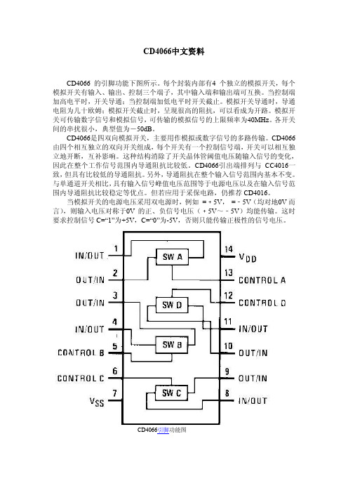
当模拟开关的电源电压采用双电源时,例如 =﹢5V, =﹣5V(均对地0V 而 言),则输入电压对称于0V 的正、负信号电压(﹢5V~﹣5V)均能传输。这时 要求控制信号 C=“1”为+5V,C=“0”为-5V,否则只能传输正极性的信号电压。
CD4066引脚功能图
内部方框图
Absolute Maximum Ratings 绝对最大额定值:
5
=50pF(Figure 6)
0
RL=1.0kΩ, CL=50pF, (Figure 7)VOS(f) = ½ VOS(1.0 kHz)
6. VDD = 5.0V
0
8. VDD = 10V
0
8. VDD = 15V
5
Signal
Input
CIS Capacitance 信 号
8.
输入电容
0
Signal
20
80 240
320
0
Δ“ON”
RL = 10kΩ to (VDD − VSS/2) VCC = VDD, VIS = VSS to VDD
ΔRO Resistance
VDD = 10V
10
N Between Any 2
MAX465中文资料

PART
DESCRIPΒιβλιοθήκη IONMAX463 MAX464 MAX465 MAX466 MAX467 MAX468 MAX469 MAX470
Triple RGB Switch & Buffer Quad RGB Switch & Buffer Triple RGB Switch & Buffer Quad RGB Switch & Buffer Triple Video Buffer Quad Video Buffer Triple Video Buffer Quad Video Buffer
Continuous Power Dissipation (TA = +70°C) 16-Pin Plastic DIP (derate 22.22mW/°C above +70°C) ....1778mW 16-Pin Wide SO (derate 20.00mW/°C above +70°C) .......1600mW
The MAX463–MAX470 series of two-channel, triple/quad buffered video switches and video buffers combines high-accuracy, unity-gain-stable amplifiers with high-performance video switches. Fast switching time and low differential gain and phase error make this series of switches and buffers ideal for all video applications. The devices are all specified for ±5V supply operation with inputs and outputs as high as ±2.5V when driving 150Ω loads (75Ω back-terminated cable).
LD4606A资料

DATA SHEETDocument No. ET0117EJ3V1DS00 (3rd edition)Date Published August 1998 M Printed in Japan30 GHz, 380 W CW, HIGH EFFICIENCY , HIGH POWER GAINThe information in this document is subject to change without notice.©1989LD4606AFor safe use of microwave tubes, refer to NEC document “Safety instructions to all personnel handling electron tubes” (ET0048EJ ∗V ∗UM00)GENERAL DESCRIPTIONThe NEC LD4606A is a five-cavity Klystron amplifier and ideal for use in the earth-to-satellite communications trans-mitter.This is designed for operating at 380 W CW power lev-els in the frequency range of 27.50 to 29.10 GHz. The in-stantaneous bandwidth of minus one-decibel is at least 70 MHz over the entire 1.6 GHz range.The tube is forced-air-cooled at the 380 W operation.Furthermore, this is of rugged and reliable design of-fering long-life service.FEATURES1High EfficiencyThe DC to RF conversion efficiency is typically 23 %by incorporating a 39 % depressed collector.2High Power GainThe power gain is typically 40 dB at the 380 W level,so the driving power is less than 50 mW.3Simple Cooling SystemThe klystron is all forced air cooled with only one blower, so that the cooling systems are greatly sim-plified.4Permanent MagnetThe klystron is permanent magnet focused, eliminat-ing entirely the requirement for focusing power sup-plied and interlock circuits.5Rugged ConstructionThe klystron is designed to be rugged.2LD4606AGENERAL CHARACTERISTICSELECTRICALFrequency………………………………………………27.50 to 29.10 GHzOutput Power…………………………………………380 WHeater Voltage………………………………………… 4.3 VHeater Current………………………………………… 2.5 AType of Cathode………………………………………Indirectly Heated, ImpregnatedMECHANICALDimensions……………………………………………See OutlineFocusing………………………………………………Permanent MagnetElectrical ConnectionsHeater………………………………………………AMP (861647-8) ReceptacleHeater-Cathode……………………………………AMP (861647-8) ReceptacleBody, Collector……………………………………AMP (861647-8) ReceptacleRF ConnectionsInput…………………………………………………Mates with FUBR-260Output………………………………………………Mates with FUBR-260Mounting Position……………………………………Vertical (Cathode down)Weight…………………………………………………45 kg approx.CoolingGun…………………………………………………Forced AirCollector……………………………………………Forced AirBody…………………………………………………Forced AirCavity Tuning Method………………………………Hand TuningABSOLUTE RATINGS ( Note 1, 2 and 3 )ELECTRICAL Min.Max.UnitHeater Voltage………………………………………… 3.5 5.5VHeater Surge Current………………………………– 5.5AHeater Warm-up Time………………………………300–sBody Voltage…………………………………………–9.5kVCollector Voltage………………………………………–9.0kVBeam Current…………………………………………–400mABody Current…………………………………………–20mACollector Current………………………………………–400mADC Input Power………………………………………– 2.5kWLoad VSWRNormal Value………………………………………– 1.2Instantaneous Value………………………………– 1.5MECHANICALCollector Temperature………………………………–200°CCooling Air Temperature……………………………–1045°CAir Flow for Collector Body and Gun……………238–kg/hrAmbient TemperatureOperating……………………………………………–1045°CStorage………………………………………………–4070°CTYPICAL OPERATION (Note 3, 4 and 5)UnitFrequency………………………………………………………28.5GHzHeater Voltage (Note 4)……………………………………… 4.3VHeater Current………………………………………………… 2.5ABody Voltage……………………………………………………8.5kVBody Current……………………………………………………10mACollector Voltage……………………………………………… 5.2kVCollector Current………………………………………………300mADC Input Power……………………………………………… 1.65kWDriving Power…………………………………………………44mWOutput Power…………………………………………………380WPower Gain……………………………………………………40dBBand Width (-1 dB)……………………………………………80MHzAir Flow of Collector, Body and Gun………………………250kg/hrNote 1 :Absolute rating should not be exceeded under continuous or transient conditions. A single absolute rating may be the limitation and simultaneous operation at more than one absolute rating may not bepossible. Equipment design should limit voltage and environmental variations so that ratings will beexceeded.Note 2 :The Klystron body should be at ground potential in operation.Note 3 :All voltages are referred to the cathode potential except the heater voltage.Note 4 :The optimum operating value is shown on a test performance sheet for each tube.Note 5 :Characteristics and operating values on this Data Sheet are based on performance test. These values may be changed as a result of additional information or product improvement. NEC should be con-sulted before using this information for equipment design. This data sheet should not be referred to acontractual specification.No part of this document may be copied in any form or by any means without the prior written consent of NEC Corporation.NEC Corporation does not assume any liability for infringement of patents, copyrights or other intellectual property rights of third parties by or arising from use of a device described herein or any other liability arising from use of such device. No license, either express, implied or otherwise, is granted under any patents, copy-rights or other intellectual property rights of NEC Corporation or of others.3LD4606A OUTLINE (Unit in mm)。
MAX4376FAUK中文资料

GAIN
SUFFIX
20
T
50
F
100
H
For example, MAX4376TAUK is a single high-side amplifier with a gain of 20.
High-side current monitoring is especially useful in battery-powered systems since it does not interfere with the ground path of the battery charger. The input common-mode range of 0 to +28V is independent of the supply voltage and ensures that the current-sense feedback remains viable even when connected to a battery pack in deep discharge.
-40°C to +125°C -40°C to +125°C -40°C to +125°C -40°C to +125°C -40°C to +125°C -40°C to +125°C
5 SOT23-5 5 SOT23-5 5 SOT23-5 8 SO 8 SO 8 SO
ADOG ADOH ADOI
Applications
Notebook Computers
Current-Limited Power Supplies
Fuel Gauges in PC
General-System/BoardLevel Current Monitoring
- 1、下载文档前请自行甄别文档内容的完整性,平台不提供额外的编辑、内容补充、找答案等附加服务。
- 2、"仅部分预览"的文档,不可在线预览部分如存在完整性等问题,可反馈申请退款(可完整预览的文档不适用该条件!)。
- 3、如文档侵犯您的权益,请联系客服反馈,我们会尽快为您处理(人工客服工作时间:9:00-18:30)。
SYMBOL
CONDITIONS
MIN
VCOM_,VNO_, SHDN or SHDN/EN = 0 (Note 3)
0
VNC _
VFP
3.6
RON
ICOM_ = -40mA,
TA = +25°C
0V ≤ VCOM_≤ V+, SHDN or SHDN/EN = 0
TA = TMIN to TMAX
100mV/div
Pin Configurations
TOP VIEW
IN 1 SHDN/EN 2
GND 3 COM1 4 COM2 5
MAX4906 MAX4906F
10 V+ 9 NC1 8 NC2 7 NO1 6 NO2
500ps/div
VNO2OUT
μDFN Pin Configurations continued at end of data sheet.
ELECTRICAL பைடு நூலகம்HARACTERISTICS
(V+ = +3V to +3.6V, TA = TMIN to TMAX, unless otherwise noted. Typical values are at V+= 3.3V, TA = +25°C.) (Note 2)
PARAMETER ANALOG SWITCH Analog Signal Range Fault-Protection Trip Threshold
10 µDFN
L1022-1
MAX4906FELB
10 µDFN
L1022-1
MAX4907ELA
8 µDFN
L822-1
MAX4907FELA
8 µDFN
L822-1
Note: All devices operate over the -40°C to +85°C operating temperature range.
TYP MAX
V+
4.0
4
7
8
On-Resistance During Shutdown
RONSH
ICOM_ = -40mA, 0V ≤ VCOM_ ≤ 1.5V, SHDN = V+
(MAX4907/MAX4907F)
TA = +25°C TA = TMIN to TMAX
4
10
13
On-Resistance Match Between Channels
Note 1: Signals on IN, SHDN or SHDN/EN exceeding V+ or GND are clamped by internal diodes. Limit forward-diode current to maximum current rating.
Stresses beyond those listed under “Absolute Maximum Ratings” may cause permanent damage to the device. These are stress ratings only, and functional operation of the device at these or any other conditions beyond those indicated in the operational sections of the specifications is not implied. Exposure to absolute maximum rating conditions for extended periods may affect device reliability.
Shorts to USB Supply Rail Up to +5.5V ♦ Space-Saving Packages
8-Pin and 10-Pin, 2mm x 2mm µDFN Packages
Ordering Information
PART
PIN-PACKAGE
PKG CODE
MAX4906ELB
(pulsed at 1ms 10% duty cycle).................................±240mA
Continuous Power Dissipation (TA = +70°C) 8-Pin µDFN (derate 5.0mW/°C above +70°C) .............400mW 10-Pin µDFN (derate 5.3mW/°C above +70°C) ........423.7mW
Cell Phones PDAs Digital Still Cameras GPS Notebook Computers Relay Replacements
USB Switching Ethernet Switching Video Switching Bus Switches T3/E3 Switches for Redundancy Protection
Operating Temperature Range ..........................-40°C to +85°C Junction Temperature .....................................................+150°C Storage Temperature Range .............................-65°C to +150°C Lead Temperature (soldering, 10s) .................................+300°C
Features
♦ Fully Specified for a Single +3.0V to +3.6V Power-Supply Voltage
♦ Low 4Ω (typ), 7Ω (max) On-Resistance (RON) ♦ MAX4907/MAX4907F Ultra-Low 4pF (typ),
________________________________________________________________ Maxim Integrated Products 1
For pricing, delivery, and ordering information, please contact Maxim/Dallas Direct! at 1-888-629-4642, or visit Maxim’s website at .
The MAX4906/MAX4906F feature two single-pole/double-throw (SPDT) switches, and the MAX4907/ MAX4907F feature two single-pole/single-throw switches (SPST). The MAX4907/MAX4907F have a low 7Ω (max) on-resistance and 7pF (max) on-capacitance. These devices are fully specified to operate from a single +3.0V to +3.6V power supply and are protected against a +5.5V short to COM1 and COM2. This feature makes them fully compliant with the USB 2.0 specification of +5.5V fault protection. These devices feature a low threshold voltage and a +1.4V VIH, permitting them to be used with low-voltage logic. The MAX4906/ MAX4906F/MAX4907/MAX4907F operate at 300µA (max) quiescent current and feature a shutdown input to reduce the quiescent current to less than 2µA (max).
ΔRON
V+ = 3.0V, ICOM_= -40mA, VCOM_ = 1.5V (Note 4)
The MAX4906/MAX4906F/MAX4907/MAX4907F are available in space-saving, 2mm x 2mm µDFN packages and operate over a -40°C to +85°C temperature range.
Applications
Selector Guide appears at end of data sheet.
Typical Operating Characteristics
EYE DIAGRAM
V+ =3.3V IBIAS = 9mA f = 240MHz
VNO1OUT
USB 2.0 HIGH SPEED TRANSMIT TEMPLATE
7pF (max) On-Capacitance (CON) ♦ -3dB Bandwidth: 1GHz (typ) ♦ Low Bit-to-Bit Skew ≤ 100ps ♦ Shutdown Input Reduces Power Consumption