[原创] 分享调试SI4432的一些小经验
基于Si4432的温湿度采集电路设计与实现
信息工程学院本科毕业论文(2013届)题目基于Si4432的温湿度采集电路设计与实现系电子工程专业电子信息科学与技术班级09091912学号09919227学生姓名王超超指导教师孔庆鹏完成日期2012年12月诚信承诺我谨在此承诺:本人所写的毕业论文《高灵敏度授时信号接收系统》均系本人独立完成,没有抄袭行为,凡涉及其他作者的观点和材料,均作了注释,若有不实,后果由本人承担。
承诺人(签名):年月日摘要温湿度的自动测量和显示记录是工厂的一项常规监测项目。
以往的人工采集数据占用人力资源,可靠性低,容易发生差错已经不适应工业化生产的要求了。
一般的温湿度采集系统数据显示单调,缺乏支持各种PLC的通讯端口,而且温湿度采集模块布线繁琐且受原有车间布局的约束。
本文采用目前应用广泛的ARM系列微处理器ATMEGA48作为平台的核心构建系统。
发射板:温湿度采集器以ATMEGA88作为主控制芯片,采用数字温湿度传感器芯片SHTl0采集外界温湿度值。
然后通过无线射频收发器SI4432将数据发送到发射板。
接收板:以ATMEGA88作为主控制芯片使无线射频收发器SI4432所接收到的温湿度的数据显示在LCD1602显示屏上,省去了冗长且铺设不便的通讯电缆。
本项目的硬件设计任务包括:设计目标,主机以及温湿度采集模块的器件选型以及原理图设计,PCB板的设计指示,测试以及调试。
关键词:ATMEGA48;SHT10;SI4432;LCD1602ABSTRACTThe automatic-measure and the records display of temperature and humidity is one of the conventional monitoring projects in the factory. In the past, people collected data themselves. In this way, it needed much human resource with low reliability. Of course error is easy to happen. So this way was not fit to the requirements of industrial production. General temperature and humidity collection system display data monotonous and short of history data. Many of these systems also don’t support the communication with most of PLC. Furthermore, temperature and humidity collection module is difficult to layout as too many lines.It is restricted by the placement of plant also.This paper utilizes ARM micro-processor‘ATMEGA48’as the core ofthe platform to buildup system, which is applied widely at present.Transmitter board: temperature and humidity logger ATMEGA88 as the main control chip, digital temperature and humidity the sensor chip SHTl0 acquisition outside temperature and humidity valued. Then through the radio frequency transceiver SI4432 data will be sent to launch plate. Receiving plate: ATMEGA88 the wireless RF transceiver as the primary control chip SI4432 received by the temperature and humidity data LCD1602 display, eliminating the a lengthy and laying inconvenience communication cable.The hardware design tasks of the project include: design goals, the host, as well as temperature and humidity acquisition module device selection and schematic design, PCB board design instructions, testing, and debugging.Key words:ATMEGA48;SHT10;SI4432;LCD1602目录1 引言 (1)2 概述 (2)2.1 无线温湿度采集概述 (2)2.2 本设计方案思路 (4)2.3 研发方向和技术关键 (4)3 总体设计 (7)3.1电源模块 (7)3.2微控制器系统 (8)3.3无线温湿度检测系统 (8)4 硬件设计 (10)4.1 电源转换 (10)4.2 微控制器系统 (11)4.3 温湿度采集模块 (14)4.4 无线收发模块 (18)5软件设计 (21)5.1 总方案流程 (21)5.2 程序流程图 (21)5.3 模块说明 (22)6 制作与调试 (24)6.1 PCB制作与程序编写 (24)6.2 系统调试 (25)6.3 其他 (27)7结束语 (28)致谢 (29)参考文献 (29)附录一 (30)附录二 (32)附录三 (34)1 引言温度和湿度与工农业及人民的普通生活有着密切联系。
原文(Si4432资料)

1、DETAILED DESCRIPTIONSilicon Labs‟ IA4432 transceiver is a member of the newEZRadioPROTM family. While retaining all the attractive features ofearlier products such as high integration, low cost, flexibility, lowBill of Materials (BOM) cost, and easy design-in, these parts aretargeted to more sophisticated applications and offer severalenhanced parameters and features, including continuousfrequency coverage from 240-930MHz and output power up to+20dBm. Also included are built-in features like wake-up timer, lowbattery detector, temperature sensor, general purpose Analog toDigital Converter (ADC), TX/RX First-In First-Out Buffers (FIFO‟s),power-on-reset (POR), and general purpose I/Os (GPIOs). The chipincorporates a high performance ADC in the RX path and digitalmodem which performs demodulation, filtering, and packethandling in the digital domain making it ideal for configuration tomultiple applications. These features simplify the task of thesystem designer and allow for the use of lower-endMicrocontrollers. A highly efficient +20dBm power amplifier (PA) is,completely integrated which eliminates the need for an external PA,and makes the part ideal for Frequency Hopping Systems where maximum range is desired. The devices comply with FCC andETSI,requirements when used in any of the standard ISM bands. Onlya,30MHz crystal and a limited number of passivematching/filtering,components are necessary as external components making the,device ideal for high volume production i n applications where size,and cost are critical.The IA4432 is a CMOS Radio Frequency Integrated circuitwhich incorporates all of the transmit and receive functionsrequired for ISM band applications. The chip is designed tooperate over a wide range of freq uencies, voltages, andtemperature with extremely low current consumption whichmakes it ideal for low-data rate battery powered applications.The protocol used by the system utilizes Time DivisionDuplexing (TDD), in which the transceiver alternately transmitsand receives in a burst-like nature. Thereceive path uses asingle-conversion architecture which image-reject mixes the2-level FSK/GFSK/OOK modulated receive signal to a low IFfrequency. Following a programmable gain amplifier (PGA) thesignal is converted to the digital domain by a high performanceΣΔ ADC so filtering, demodulation, slicing, error correction, andpacket handling are performed in the digital domain where theycan be done more efficiently. The resulting demodulated signalis then output to the Microcontroller through a programmableGPIO or over the standard SPI bus by reading the FIFO.A single local oscillator (LO) is used for both transmit andreceive modes since the transmitter and receiver are never onat the same time. The LO is generated by an integrated VCOand ΣΔ Fractional-N PLL synthesizer. The synthesizer isdesigned to allow for configurable data rate, output frequency,frequency deviation, and Gaussian Filtering at any frequencybetween 240-930MHz. The transmit FSK data is modulateddirectly into the Δ-Σdata stream. The data may shaped by aGaussian low-pass filter to achieve a more desirable spectrum.The PA exhibits a maximum output power of +20dBm. Theoutput power is configurable between +11 and +20dBm in 3dBsteps. The PA is single-ended to allow for easy matching andlow BOM cost. The PA incorporates its own ramp-up and rampdownof the burst signal to prevent unwanted spectral splatter.With the integrated +20dBm PA, easy frequency hoppingcontrol, TXRX switch control, and antenna diversity switchcontrol, significant advantages can be achieved. AntennaDiversity is completely integrated into the IA4432 and canimprove the system link budget by 8-10dB in a typicalenvironment. Antenna diversity can improve the range by 50-100% depending on the environment. The +20dBm poweramplifier can also be used to compensate for a lower cost,lower performance antenna reducing the overall system costand geometrical size but still achieving maximum range.2、FUNCTIONAL DESCRIPTIONThe IA4432 is designed to work with a Microcontroller, crystal, and a few passives to create a very low cost system as shown Figure1. Voltage regulators are integrated on-chip which allow for a wide range of operating supply voltage conditions from +1.8 to +3.6V.A standard four pin SPI bus is used to communicate with the Microcontroller. Three configurable general purpose I/Os are availablefor use to tailor towards the needs of the system. A more complete list of the available GPIO functions is shown in section 9 AuxiliaryFunctions but just to name a few, Microcontroller clock output, Antenna Diversity, TRSW control, POR, and specific interrupts. Alimited number of passive components are needed to match the LNA and PA; refer to Section 11, Reference Design for the requiredcomponent values at different frequency ranges.The application below is designed for a system with Antenna Diversity. Using Antenna Diversity can increase the link budget of thesystem by as much as 10dB. The Antenna Diversity Control Algorithm is completely integrated into the chip and is discussed furtherin Section 9.8Antenna-Diversity.2.3 Operating ModesThe following table summarizes the modes of operation of the RFIC. In general, any given mode of operation may be classified as anActive mode or a Power Saving mode. The table indicates which block(s) are enabled (active) in each corresponding mode. With theexception the Shutdown mode, all can be dynamically selected by sending the appropriate commands over the SPI in order tooptimize th e average current consumption. An “X” in any cell means that in the given mode of operation that block can beindependently programmed to be either ON or OFF, without noticeably affecting the current consumption. The SPI circuit blockincludes the SPI interface and the Register Space. The 32kHz OSC circuit block includes the 32.768KHz RC oscillator or 32.768KHzCrystal Oscillator, and Wake-Up-Timer. AUX (Auxiliary Blocks) includes the Temperature Sensor, General Purpose ADC, and Low-Battery Detector.4 CONTROLLER INTERFACE4.1 Serial Peripheral Interface (SPI)The control logic is designed to accept data over a 3 wire SPI interface, SCLK, SDI, and nSEL. The control logic will also read out datafrom internal registers on a fourth SDO output pin. AN SPI transaction is a 16 bit sequence which consists of a Read-Write (RW)select bit, followed by a 7 bit addressfield(ADDR), and an 8 bit data field(DATA), as demonstrated in Figure 4. The 7 bit address fieldsupports reading from or writing to one of the 128, 8-bit control registers. The RW select bit determines whether the SPI transactionis a write or read transaction. If RW=1 it signifies a WRITE transaction and if RW=0 then it signifies a READ transaction. The contents(ADDR or DATA) are latched into the digi tal block every eight clock cycles. The timing parameters for the SPI interface are shown inthe Serial Interface Timing Parameters Table below. The clock rate for SCLK is flexible with a maximum rate of 10MHz.The SPI may also be used to read data back from the RFIC. In order to read back data from the RFIC the RW bit must be set to …0‟followed by the 7-bit address of the register from which to read. The 8 bit DATA field following the 7 bit ADDR field is ignored whenRW=‟0‟. The next eight positive edge t ransitions of the SCLK signal will clock out the contents of the selected register. The dataread from the selected register will be available on the SDO output pin. The READ function is shown in Figure 5 below. After theREAD function is completed the SDO p in will remain at either a logic …1‟ or logic …0‟ state depending on the last data bit clocked out(D0). When nSEL goes high the SDO output pin will be pulled high by internal pull-up. The SPI interface contains a burst read/write mode which will allows for reading/writing sequential registers without having to resendthe SPI address. When the nSEL bit is held low while continuing to send SCLK pulses, the SPI interface will automaticallyincrement the ADDR and read from/write to the next address. An SPI Burst Write transaction is demonstrated in Figure 6, and burstread in Figure 5. As long as nSEL is held low, input data will be latched into the digital block every eight SCLK cycles. A Burst ReadTransaction is also demonstrated in Figure 74.2 Operating Mode ControlThere are four main states in the Main State Machine, SHUTDOWN, IDLE, TX, and RX (see Figure 8:). The SHUTDOWN statecompletely shuts down the radio to minimize current consumption. There are five different configurations/options for the IDLE statewhich can be selected to optimize the chip to the applications needs. SPI Registers 07h controls which operating mode/state isselected. The TX and RX state may be reached automatically from any of the IDLE states by selecting either the txon or rxon bits. Table 11: shows each of the operating modes with the time required to reach either RX or TX mode as well as the currentconsumption of each mode.The shutdown state is the lowest current consumption state of the chip with nominally only 5nA of current cons umption. Theshutdown state may be entered by setting the SDN pin (Pin 20) =‟1‟. The SDN pin should be = …0‟ in all states except SHUTDOWNstate. In SHUTDOWN state the contents of the registers are lost and there is no SPI access.When the chip is connected to the power supply, a POR will be initiated after the falling edge of SDN.There are five different modes in the IDLE state which may be selected by the SPI Register, 07h. All of the modes have a differenttradeoff between current consumption and response time to TX mode. This isshown above in Table 11:. After the POR event,SWRESET, or exiting from the SHUTDOWN state the chip will default to the IDLE-READY mode.STANDBY mode has the lowest current consumption possible with only the LPLDO enabled to mainta in the SPI register values. Inthis mode the registers can be accessed in both read and write mode. The standby mode can be entered by writing 0h to register07h. If an interrupt has occurred (i.e. the nIRQ pin = …0‟) the interrupt registers must be read to achieve the minimum currentconsumption. Also, the ADC should not be selected as an input to the GPIO in this mode and will cause excess current consumption.In SLEEP mode the LPLDO is enabled along with the Wake-Up-Timer, which can be used to accurately wake-up the radio at specifiedintervals. See section 9.6 for more information on the Wake-Up-Timer. Sleep mode is entered by setting enwt=‟1‟ (40h) in register07h. If an interrupt has occurred (i.e. the nIRQ pin = …0‟) the interrupt registers must be read t o achieve the minimum currentconsumption. Also, the ADC should not be selected as an input to the GPIO in this mode and will cause excess current consumption.In SENSOR Mode either the Low Battery Detector, Temperature Sensor, or both may be enabled in addition to the LPLDO and Wake-Up-Timer. The Low Battery Detector may be enabled to settingenlbd=‟1‟ and the temperature sensor can be enabled by settingents=‟1‟ in register 07h. See sections 9.4 and 9.5 for more information on these features. If an interrupt has occurred (i.e. the nIRQ pin = 0) the interrupt registers must be read to achieve the minimum current consumption.READY Mode is designed to give fast res ponse time to TX mode with reasonable current consumption. In this mode the Crystaloscillator remains enabled reducing the time required to switch to either TX mode by eliminating the crystal start-up time. Readymode is entered by setting xton =‟1‟ in regi ster 07h. To achieve the lowest current consumption state the crystal oscillator buffershould be disabled. This is done by setting the value of register 62h to a value of 02h. To exit ready mode bit 2 of this register mustbe set back to 0.In TUNE Mode the PLL remains enabled in addition to the other blocks which are enabled in the other IDLE Modes. This will give thefastest response to TX mode because the PLL will remain locked but it comes at the price of the highest current consumption. Thismode of operation is designed for Frequency Hopping Systems. Tune mode is entered by setting pllon = …1‟ in register 07h, i.e. thevalue of register 07h should be 02h. It is not necessary to set xton to …1‟ for this mode, the internal state machine knows that thecrystal oscillator needs to be running in this mode and will enable it automatically.The TX state may be entered from any of the Idle Modes when the txon bit is set to …1‟ in SPI Register 07h. A built-in sequencer takescare of all the actions required to transition between states from enabling the Crystal Oscillator to ramping up the PA to preventunwanted spectral splatter. The followingsequence of events will occur automatically when going from STANDBY mode to TX modeby setting the txon bit.1. Enable the Main Digital LDO and the Analog LDOs2. Start up crystal oscillator and wait until ready (controlled by timer)3. Enable PLL4. Calibrate VCO (this action is skipped when the vcocal bit is “0”, default value is “1”)5. Wait until PLL settles to required transmit frequency (controlled by timer)6. Activate Power Amplifier and wait until power ramping is completed (controlled by timer)7. Transmit PacketThe first few steps may be eliminated depending on which IDLE mode the chip is configured to prior to setting the txon bit. Bydefault, the VCO and PLL are calibrated every time the PLL is enabled. If the ambient temperature is constant and the samefrequency band is being used these functions may be skipped by setting the appropriate bits in SPI Register 55h.Th e RX state may be entered from any of the Idle modes when the rxon bit is set to …1‟ in the SPI Register 07h. A built-in sequencertakes care of all the actions required to transition from one of the IDLE modes to the RX state. The following sequence of events willoccur automatically to get the chip into RX mode when going from STANDBY mode to RX mode by setting the rxon bit:1. Enable the Main Digital LDO and the Analog LDOs2. Start up crystal oscillator and wait until ready (controlled by timer)3. Enable PLL4. Calibrate VCO (this action is skipped when the vcocal bit is “0”, default value is “1”)5. Wait until PLL settles to required transmit frequency (controlled by timer)6. Enable receive circuits: LNA, mixers, and ADC7. Calibrate ADC (RC calibration)8. Enable receive mode in the Digital ModemDepending on the configuration of the radio all or some of the following functions will be performed automatically by the DigitalModem: AGC, AFC (optional), update status registers, bit synchronizati on, packet handling (optional) including sync word, headercheck, and CRC.1、详细描述Si4432收发器是新的EZRadioPRO系列产品中的新产品,它保留了以前产品的所有优越特点,比如:高集成度、低成本、灵活性,外围精简和很容易设计等特点。
基于SI4432的915MHz射频读卡器设计

模块 、 口通 信模 块 、 示模块 和天线模块组 成。读卡 器辐射 串 警
的 高频 载 波 使 进 入 天 线 市 场 范 围 内 的 电子 标 签 从 辐 射 的 能 量
《 装备制造技术}00年第 6 21 期
基 于 SI4 2的 9 MH 43 1 5 z射 频 读 卡 器 设 计
姜
( 广西大学
摘
龙 , 国进 , 李 陈润 设
电气 与工程学 院, 广西 南 宁 5 0 0 ) 3 0 4
要 : Fecl公 司的 单片机 MC9 1 XS2 用 rea e S 2 18为控制核 心 , Sio L b 公 司的 S4 3 以 icn a s l I4 2芯 片设计制 作模 块做 射 频收发 器 , 并给 出
MC U模块选 用 Fecl 公 司的单片 机 MC S 2X 18 单 rea e 9 1 2 , S 片机 具有 6 4—2 6 B嵌入 式 闪存 , 5k 带纠 错码 ( C 功能 , E C) 4 1k 2 B的 R M, 达 4~8 B的 dt f s , 子上 集成 了 E C A 高 k a - ah 片 al C
遥测 、 门禁 系统 、 身份 识别 、 非接 触 R F智 能 卡 、 线 4 52 2 无 8 /3 数 据通信 、 全防火等领域 。 安
高频功率放 大器 、低 噪声放大器 、 Q转换 混频器 、基 带滤波 U
器、 放大器 等所需要 去 R F功能模 块 , 外部 仅仅需要 一块 晶振
模 块 、一 个 穿 行 外 设 接 口 S I 块 、 外 部 事 件 触 发 中断 输 P模 4路 入 端 口等 外 围 接 口 , 得 电 路 设 计 简 单 、 干 扰 能 力 强 。通 过 使 抗
基于Si4432的温室环境监测无线组网模块设计

基于Si4432的温室环境监测无线组网模块设计陈慧;吴次南;刘泽文【摘要】采用PIC24FJ64微处理器和Si4432无线收发芯片设计了无线组网模块,利用此无线组网模块搭建了温室控制器、数据采集器电路并编写了组网通信协议和上位机显示界面程序.该系统具有功耗低,数据可靠性高、适用性好的特点.经实际测试,系统休眠电流为4.5μA,空中传输速率是9.6 kbps,通信距离在空旷条件下可达1000 m.%In the paper,the wireless networking module is designed with PIC24FJ64 microprocessor and Si4432 wireless transceiver chip. The greenhouse controller and the data collector circuit are used to set up the network communication protocol and the host computer display interface program.The system has the characteristics of low-power consumption,high data reliability and high applicability.The experiment results show that the system sleep current is 4.5 μA,the air transfer rate is 9.6 kbps,the communication distance in the open condition is up to 1000 m.【期刊名称】《单片机与嵌入式系统应用》【年(卷),期】2018(018)001【总页数】4页(P45-47,72)【关键词】无线传感器网络;Si4432;无线组网;温湿度检测【作者】陈慧;吴次南;刘泽文【作者单位】贵州大学大数据与信息工程学院,贵阳 550025;贵州大学大数据与信息工程学院,贵阳 550025;清华大学【正文语种】中文【中图分类】TP27引言随着物联网的兴起,将无线传感器网络技术应用于温室环境监控系统成为农业研究的热门方向。
基于Si4432的无线传输模块制作
学术论丛基于Si4432的无线传输模块制作杨梦梦王俊亓刘长宇黑龙江八一农垦大学摘要:随着计算机技术、数字信息化产品的快速发展和日益丰富,数据透明传输越来越占据重要地位。
对于传统数据传输一般使用短距离RS232/RS485进行有线传输。
本设计采用将RS232串口转换为基于Si4432的无线透明传输的方式,相对于传统有线传输方式具有传输距离远、方便、快速等特点,节省了成本并且降低了用户数据传输的难度。
关键词:Si4432;无线透明传输;STC89C52单片机伴随电子半导体技术和数字化时代的不断发展,无线射频数据传输技术在现代生产和生活中的应用越来越广泛。
无线透明传输方式也变得越来越广泛。
透明传输,即不管传的数据是什么,所采用的设备只是起一个通道作用,把要传输的内容完好的传到对方。
一、国内外研究现状与发展状态串口传输为短距离传输,在短距离通信系统中应用无线代替有线的方式,在国内外早有研究。
在电子技术飞速发展的今天人们对无线通信的成本、质量、方便程度有了更高的要求。
为了替代有线传输解决布线以及应用的困难,相继有许多公司开发了串口无线透传模块来代替串口有线传输,例如蓝牙、WLAN 、射频等。
但是通过蓝牙以及WLAN 开发串口无线透传过于复杂且成本也过于高昂,开发周期也比较长。
在实现串口的数据透传功能方面,射频技术由于它的低功耗、低成本等优点被越来越多的使用。
Silicon Labs 公司推出集成度高、低功耗、多频段、低成本的Si4432无线收发芯片就成为了实现数据无线数据透传功能的很好的选择。
在控制器选择方面,很多开发者使用MSP 或者更好的控制器芯片,然而这些芯片并不利于初学者开发使用,本设计采用STC89C52单片机控制有利于初学者在其基础上进行二次开发二、控制器单元电路设计控制单元核心采用STC89C52RC 单片机进行控制。
控制单元的电路由复位电路、晶体震荡电路组成。
单片机的复位就需要手动按下复位按钮,使得复位按钮产生一个持续2us 以上的高电平输入到STC89C52RC 芯片复位端,当RST 端接收到高电平之后才可使其正常复位。
SI4432数传模块规格书
条件
@20dBm
414.92 433.92 453.92 MHZ
频率范围 (不同规格)
470.92 470.92 849.92 868.92
509.92 888.92
MHZ MHZ
895.92 914.92 934.92 MHZ
调制速率
1.2
ቤተ መጻሕፍቲ ባይዱ
9.6
38.4
Kbps
发射功率范围
-1
/
+20
dBm
接收灵敏度
模块内部设有 200 字节的缓冲区,当串口数率小于等于无线传输速率时可保证数据的传 输顺畅,但若串口速率大于无线传输速率时,连续发送数据字节数超过缓冲区大小则可能会 出现数据溢出而导致的数据丢失现象。因此如需连续发送大量数据时,为避免数据丢失或错 误,可在设置参数时使串口传输速率不超过无线传输速率。
七、 典型应用电路
TEL:075536938056 13570812706
第5页共8页
深圳市凌承芯电子有限公司
八、 脚位定义
脚位编号 引脚定义
描述
1
VCC 接电源正极(典型值 5V)
2
GND 接电源地
3
TXD 串口通讯数据发射
4
RXD 串口通讯数据接收
5
SET 配置参数使能(低电平使能参数配置,默认高电平输出)
二、 特点
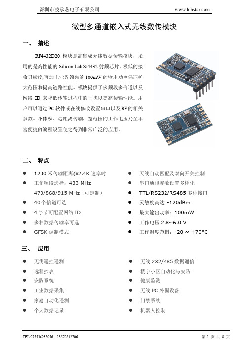
1200 米传输距离@2.4K 速率时 工作频段选择:433 MHz
470/868/915 MHz(可定制) 40 个信道可选 4 字节可配置网络 ID 多种数据传输率可选 GFSK 调制模式
三、 应用
无线遥控遥测 远程抄表 安防系统 工业数据采集 家庭自动化遥测 个人数据记录
基于SI4432的无线收发平台设计
基于SI4432的无线收发平台设计陈继磊;祁云嵩;徐钊【摘要】文中采用低成本、低功耗STM8L151作为控制器,高性能、高集成度的射频芯片SI4432作为收发芯片.同时改进了冲突退避算法,考虑当前网络状态,引入概率机制合理选择随机退避时间区间,减少数据包碰撞几率,降低了丢包率.结合实际环境,兼顾接收信号强度指示器(RSSI)阈值与覆盖范围的大小,计算最优发射功率,降低功耗.%In this paper, low-cost and low-power consumption STM8L151 was used as MCU, and high-performance and highintegrate SI4432 was used as transceiver. In order to decrease the data loss caused by data conflict, considering that the cur-rent network status and probability mechanism were introduced to reasonable change back off time interval,back off algorithm was improved. In order to reduce power consumption, the optimize transmission power was calculated following the RSSI threshold and the range of coverage in actual environment.【期刊名称】《仪表技术与传感器》【年(卷),期】2016(000)007【总页数】5页(P60-63,67)【关键词】STM8L151;SI4432;退避算法;最优发射功率【作者】陈继磊;祁云嵩;徐钊【作者单位】江苏科技大学计算机科学与工程学院,江苏镇江 212003;江苏科技大学计算机科学与工程学院,江苏镇江 212003;南京理工大学计算机科学与工程学院,江苏南京 210094【正文语种】中文【中图分类】TN92随着半导体技术的发展,无线射频通信芯片向低功耗、高集成度、专业化方向发展,基于这些优势,设计了一种基于SI4432和STM8L的低成本、低功耗、高性能无线收发平台,并做了两点优化改进:改进的冲突避免退避算法;最优发射功率的计算。
E27是基于SI4432芯片的433MHz无线模块,小体积贴片型,发射功率高、接受灵敏度高、谐波小
SI4432无线模块E27系列本说明书可能会随着产品的不断改进有所更改,请以最新版的说明书为准成都亿佰特电子科技有限公司保留对本说明中所有内容的最终解释权及修改权版本修订日期修订说明维护人1.00 2017/12/05 初始版本huaa1.10 2018/01/30 型号名称变更huaa产品概述E27系列产品是成都亿佰特公司设计生产的一款433MHz射频模块,小体积贴片型(引脚间距1.27mm),最大功率20dBm。
模块自带高性能,弹簧天线,具有极好的阻抗匹配,具有发射功率高,接受灵敏度高,发射电流小,谐波小等特点。
E27系列产品采用Silicon Labs公司的SI4432射频芯片,芯片内置天线多样化和支持跳频,具有优越的抗干扰性能;同时,其内部还具有额外的功能,如:自动唤醒定时器,低电池电量检测器,64 字节发射/接收,自动数据包处理,集成温度传感器,模拟数字转化器,上电复位等等。
E27系列产品为硬件平台,出厂无程序,用户需要进行二次开发。
产品型号载波频率发射功率参考距离(PCB/IPX) 封装形式天线形式E27 (433M20S) 433M 20dBm 1600m 贴片邮票孔目录产品概述 (1)1. 技术参数 (3)1.1. E27(433M20S) (3)1.2. 参数说明 (3)2. 机械特性 (4)2.1 E27(433M20S) (4)2.1.1 尺寸图 (4)2.1.2 引脚定义 (4)3. 推荐连线图 (5)4. 生产指导 (5)2.2 回流焊温度 (5)2.3 回流焊曲线图 (6)5. 常见问题 (6)5.1. 通信距离很近 (6)5.2. 模块易损坏 (7)6. 重要声明 (7)7. 关于我们 (7)1.技术参数产品型号核心IC 尺寸模块净重工作温度工作湿度储存温度E27 (433M20S) SI4432 16 * 16 mm 0.7±0.1g -40 ~ 85℃10% ~ 90% -40 ~ 125°C1.1.E27 (433M20S)参数类别Min Typ Max 单位发射电流78 83 91 mA接收电流14.7 18.5 20.0 mA关断电流0.4 0.5 0.6 μA发射功率19 20 21 dBm 接收灵敏度-119 -121 -123 dBm 推荐工作频段425 433 525 MHz 供电电压 1.8 3.3 3.6 V通信电平 1.8 3.3 3.6 V1.2.参数说明●在针对模块设计供电电路时,往往推荐保留30%以上余量,有整机利于长期稳定地工作;●发射瞬间需求的电流较大但是往往因为发射时间极短,消耗的总能量可能更小;●当客户使用外置天线时,天线与模块在不同频点上的阻抗匹配程度不同会不同程度地影响发射电流的大小;●射频芯片处于纯粹接收状态时消耗的电流称为接收电流,部分带有通信协议的射频芯片或者开发者已经加载部分自行开发的协议于整机之上,这样可能会导致测试的接收电流偏大;●处于接纯粹收状态的电流往往都是mA级的,µA级的“接收电流”需要开发者通过软件进行处理;●当前灵敏度均为在空中速率为1kbps下测试;●关断电流往往远远小于整机电源部分的在空载时所消耗的电流,不必过分苛求;●由于物料本身具有一定误差,单个LRC元件具有±0.1%的误差,但犹豫在整个射频回路中使用了多个LRC元件,会存在误差累积的情况,致使不同模块的发射电流与接收电流存在差异;●降低发射功率可以一定程度上降低功耗,但由于诸多原因降低发射功率发射会降低内部PA的效率。
Si4432编程指南(中文)
EZRADIOPRO™ 编程指南
Coolbor Xie 翻译自 AN415 1、概述
本文档通过几个简单的软件示例,介绍了如何配置 EZRadioPRO 射频发射器、接收器和收发器操作。 本指南包括以下操作示例: z 如何使用 EZRadioPRO 发射器或收发器在 FIFO 模式下进行数据包发射; z 如何使用 EZRadioPRO 接收器或收发器在 FIFO 模式下进行数据包接收; z 如何使用 EZRadioPRO 收发器进行双向基本通信; z 如何使用 FIFO 发射和接收超过 64 字节的数据包。 最 后 一 个 示 例 程 序 源 代 码 可 以 Silicon Labs 网 站 下 载 : https:///products/wireless/EZRadioPRO/, 或在与评估板工具包一起送出的 WDS 光盘上找到。 2、硬件选项 提供两个 EZRadioPRO 收发器芯片的源代码:Si4431-A0 版和 Si4432-V2 版。 这两个器件之间有几点区别: z Si4432-V2 要求对一些寄存器进行编程为不同于其默认的值。而 Si4431-A0 则无此需要。 z Si4431-A0 有一个单独的寄存器用于自动频率调整 (Auto-Frequency Calibration) 限制; 而 Si4432-V2 则使用频率偏差(Frequency Deviation)寄存器。 z Si4431 和 Si4432 的调制解调器的参数不同。 z 无效引导码超时的定义不同。 为 Si4431 和 Si4432 所提供的源代码例程分别使用不同的高亮。Si4431 和 Si4432 器件以后的版本将共 享 Si4431-A0 相同的寄存器设置。 注意:由于本文档只介绍了 Si4431-A0 和 Si4432-V2 器件,但发射或接收软件支持 EZRadioPRO 单独 的发射器和接收器: z Si4431-A0 发射例程代码无需任何修改即可支持 Si4031-A0。代码也可应用于 Si4430-A0 或 Si4030-A0,但中心频率必须设置为相应的值。 z Si4432-V2 发射示例代码无需任何修改即可支持 Si4032-V2。 z Si4431 接收示例代码无需任何修改即可支持 Si4330-A0。 平台上每个示例都提供了一个单独的 Silicon Labs IDE 工作区。Silicon Labs IDE 文件名代表了所给代 码是为以下哪个平台所写的: z 含有“SDBC_DK3”的工作区文件名是为软件开发板(Software Development board)写的 z 含有“EZLINK”的工作区文件名是为 EZLink 平台写的。 2.1 天线选项 在 EZRadioPRO 器件内部,功放和 LNA 并没有连接。在使用 Si4431 收发器的时候,TX 和 RX 引脚 可以直接连接在一起, 而无需 RF 开关。 在使用 Si4432 最高输出功率设置时, 发射和接收引脚通过一个 SPDT (单刀双掷) RF 开关分别连接到天线。 EZRadioPRO 器件能进行 RF 开关控制。 通过将 RX State 和 TX State 信号送到任意两个 GPIO,即可自动控制 RF 开关。根据工作的模式,GPIO 控制 RF 开关自动将天线连接 到接收通道或发射通道。如果芯片未处于激活模式,GPIO 将禁止 RF 开关。 在单天线测试卡和 EZLink SIL 模块上,使用了相同的 RF 开关配置:TX State 信号送到 GPIO1,RX State 信号送到 GPIO2。 EZRadioPRO 一个关键的优点在于内置天线分集支持:连接两个不同极化的天线。在数据包接收的开 头,芯片对两个天线的接收信号强度进行评估,并使用较强的一个来接收数据包的剩余部分。通过选择信 号最强的天线,可以在多路径衰减和天线极化的影响存在的情况下大大提高接收器的性能。 在使用这个特性的时候,需要有一个 RF 开关将天线连接到接收或发射路径。EZRadioPRO 器件通过 任意两个 GPIO 来自动控制 RF 开关。将用于天线分集信号的天线 1 开关和用于天线分集信号的天线 2 开
4432_FSK大功率无线收发芯片
FSK大功率无线收发芯片:SI4432,发射功率+20dbm,接收灵敏度-116dbm,通讯距离2000米Silabs新推出EZradioPRO系列RFIC:IA4432,适合长远距离的无线数据传输应用.其发射功率+20dbm,接收灵敏度-116dbm,通讯距离2000米.期待于大家的合作.对于像无线抄表和汽车遥控这样的中短距离点对点或组网无线应用,系统设计师既可选择业内标准的Zigbee解决方案,也可以选择2.4GHz或1GHz以下ISM频段的专有解决方案。
但标准的Zigbee解决方案常被业内诟病为协议太复杂,实现起来不仅成本高,而且开发周期也长。
专有的2.4GHz解决方案也有实现起来成本高的弱点,因为2.4GHz频段上的干扰太多,当然它的优点是这是一个全球各国都开放的频段,因此市场空间比其它1GHz以下ISM频段来得大。
目前在2.4GHz频段上做得最好的公司是TI和欧洲的Nordic半导体公司,但在1GHz 以下ISM频段,新兴的美国Integration公司就非常值得尊敬。
该公司第二代EZRadioPRO系列无线收发器IA443X在240~960MHz频段内的最大输出功率达到了+20dBm,这意味着它的收发距离可远达2千米。
与此相对应的是,它的主要竞争对手TI目前实现的最大输出功率是+12dBm。
目前市场产品上,我们是市场上第一家能做到如此大输出功率的公司。
IA443X的主要目标应用市场是远程无线抄表、家庭安全和报警、无线PC外设、工业控制、玩具控制和远程汽车遥控等。
SILABS第一代EZRadio系列发射器和接收器的最大输出功率只有+8dBm,实际应用时它一般需要外配一个功放来增加收发距离,但SI4432高达+20dBm的输出功率使得它毋须再外配功放,这意味着SI4432可使得一个节点的系统成本再降低1美元。
此外,由于更大的收发距离意味着在同样的组网范围内可使用更少的节点或中继器,以及IA4432允许使用低成本的天线和补偿输出高功率,系统成本得到了进一步的降低。
- 1、下载文档前请自行甄别文档内容的完整性,平台不提供额外的编辑、内容补充、找答案等附加服务。
- 2、"仅部分预览"的文档,不可在线预览部分如存在完整性等问题,可反馈申请退款(可完整预览的文档不适用该条件!)。
- 3、如文档侵犯您的权益,请联系客服反馈,我们会尽快为您处理(人工客服工作时间:9:00-18:30)。
[原创] 分享调试SI4432的一些小经验
最近想做无线遥控,选用SI4432这个模块,因为这个芯片需要配置
的寄存器比较多,调试的时候遇到了很多困难,在网上搜索了很久没找到几篇好的文章。
曾多方求助,经过几天的努力终于将该模块调试成功。
在此随笔写些调试的主要步骤希望给其他开始学SI4432的人一些帮助。
另外,本人菜鸟一枚,写这篇文章目的在于避免其他新手像我一样无助,请大家多提宝贵意见,共同进步!欢迎转载。
好了,开始。
一、无线模块选型。
根据无线通讯的频段,平常用的无线模块主要有315MHZ,433MHZ,2.4GHZ。
2.4G最近貌似比较火,像24L01,好多开发板上都配这一款芯片。
433MHZ频段的模块常用的有NRF905、CC1101、SI4432。
在315MHZ频段好像做普通的遥控器比较多,像超外差模块。
本人想做无线通信,选择在2.4GHZ和433MHZ之间。
说下区别,2.4G无线通信频率高、波长短、传输速率高、绕射能力差、通信距离短。
网上卖的模块不加功率放大也就是一百米以内。
433MHZ无线通
信频率低、波长较长、传输速率低、绕射能力强、通信距离远。
价格和2.4GHZ模块相当,但是距离一般在几百米甚至更远,据说加上功率放大可达一两千米。
本人想用来遥控智能车,通信数据量不大,但是想让距离远一点。
所以选择433MHZ模块,具体型号是SI4432。
二、初次接触SI4432
该芯片价格低、传输距离远,网上用的人挺多的。
曾经找过一些资
料发现很多商业上的无线通信也是用这一款。
于是在网上买了一对,加运费一共四十多。
没有广告嫌疑,感兴趣自己搜。
买回来之后开始看相关的手册和例程。
我嘞个去,需要配置的寄存器真多,而且通讯速率、频段、前导码、同步字等等都是自己定义的,大家写的都不一样。
加上没有专业的知识,更是加大难度。
卖家配的资料室51的版本,说实话程序写的有点乱,主要是因为他们的程序是配套他们的开发板的,有很多都看不懂。
而对于我们初学者而言,最需要的却是最简单的:简单收发就行。
我使用的控制器型号:STM32F103RB。
分析了很久慢慢移植到STM32里面,失败。
多次修改,失败。
在网上搜索,网上虽然用的人多,但是资料甚少。
而且一般都是51单片机驱动的,而且是虚拟SPI!然后是几天的调试,不多说。
经过几天的调试,终于成功,下面说下使用这款芯片的要点。
三、SPI
我用的控制芯片是STM32F103RB。
SPI可以软件模拟,也可以用硬件的。
再次,建议大家用硬件的SPI,稳定,减少CPU负担。
配置硬件SPI要点:
1、速率不要太高,SI4432手册上说不要大于10MHZ。
2、MOSI、MOSO、SCK三个引脚配置为复用功能推挽输出。
3、SPI的时钟极性配置为:同步时钟的空闲状态为低电平
4、SPI的时钟的第2个跳变沿数据被采样。
(SPI_CPHA)
5、片选信号软件控制,自己定义一个IO空控制片选吧,方便。
四、硬件连接
STM32和SI4432硬件连接,具体看模块吧。
我简单说几个比较重要的
1、SI4432的SDN引脚,为高时:芯片停止工作。
为低时:芯片允许工作。
我买的模块里,这个引脚是被引出来的,别费劲了,直接接地,不要用IO口控制高低。
高手略过。
2、模块的引脚有些是2.54mm间距,有些是1.27mm。
想DIY 的朋友注意了,我当时就忘了结果买了个1.27mm的后来转接,麻烦了。
3、尽量不要用杜邦线。
我开始一直用杜邦线连起来,但是经常在发送和接收的时候出错,初始化正常。
后来用洞洞板连起来,正常。
4、SI4432是3.3V供电,电源线和地线尽量和STM32的3.3V 和地线连在一起。
不然的话容易出错,水平有限,不解释,等高人。
五、软件调试
1、SPI配置好以后,向SI4432读写数据注意地址最高位置1。
如:SPI1_ReadWriteByte(addr|0x08)
2、配置好以后,向0X00、0X01、0X02地址读取,应该有返回值,具体看手册,如果和手册上的差不多就证明SPI通讯成功了。
3、前导码个数。
SI4432_WriteReg(0x34, 0X0A); 0x34是向SI4432写入前导码的地址,0X0A是个数,但是表示其一半,也就是5个字节。
4、刚开始,不要配置帧头。
直接禁止SI4432_WriteReg(0x32, 0x00 );// 禁止帧头
5、SI4432有3个GPIO,一般自己是不用的,但是依然要配置,因为这个和模块相关。
具体问卖家。
6、SI4432主要三个状态:接收状态、发送状态、挂起状态。
发送和接收之间可以相互转换、但是转换之前需要先进入挂起状态然后至少15ms之后再进入发送或者接收状态。
程序while(1)之前最好开始就配置为挂起状态:SI4432_WriteReg(0x07, 0x01);
六、一定要多看官方的程序设计指南和芯片的手册,我会放到附件里。
以上算是对SI4432的初步认识和注意事项。
但是这些细节是比较重要的,因为像这样的无线模块最主要是先实现通讯,高级的功能慢慢调。
具体程序不再分析,我会放在附件里。
STM32F103RB,库函数。
测试多次,但是需要根据自己的模块进行调整。
快毕业了,事多,时间有限,具体看程序,多调试,多看手册。
欢迎多提意见,欢迎转载。