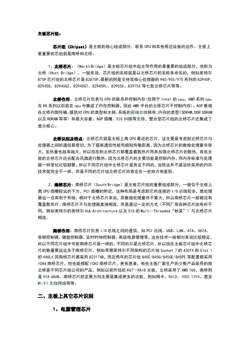
电源控制芯片W83301R
主板维修常用配件清单概要
主板维修常用配件清单主板 I/O类主板 I/O系列W83627G-AWW83627EHGW83627EHG-AW83627HG-AWW83627HF-AWW83627THFW83627THF-AW83627FW83627EHF-AW83627SFW83627GFW83637HFW83697HFW83877TFW83977EFW83977TFIT8671IT8702IT8703IT8705IT8705F-GXSIT8708IT8707IT8711IT8712F-AIT8712F-GXSIT8712F-IXSIT8712F-HXSIT8712F-AGB 技嘉专用IT8712F-SIT8716F-SIT8718F-SIT8870F-APC87364PC87366-IBW47B367PC87372IBW47M102SLPC47M10747M133-NC47M14247M17247M18247M192晶振14.318晶振32.768晶振主板电源芯片 (RT系列主板电源芯片 (RT系列RT9173RT9173B(SOP-5RT9202RT9203RT9204RT9214RT9222RT9224RT9227ART9231RT9231ART9237RT9238RT9241ART9241BRT9248RT9600RT9602RT9603主板电源芯片 (SC系列主板电源芯片 (SC系列SC1155SC1164SC1185SC1189SC1205SC1211SC2422SC2434SC2643主板电源芯片 (HIP系列主板电源芯片 (HIP系列HIP6004ECBHIP6004BCBHIP6016HIP6017HIP6018HIP6019HIP6020HIP6021ACBHIP6021CBHIP6301CBHIP6303HIP6601ACBHIP6602ACBHIP6602BCBHIP6501ACB主板电源芯片 (杂列主板电源芯片 (杂列APM7313ATXP1IRU3013RC5051RC50535090MTC5093MTCISL6524CBISL6528ISL6556BCBISL6566CR4500M(8脚贴片4501(8脚贴片4505(8脚贴片W83310S-R(8脚贴片W83301GRKA7500BL6711L6911DL6916DL6917BDL6919MS-5AS99127FUS3004LM2636LM2637LM2638LM317LM324LF353LM358LM3932030(8脚贴片时针芯片时针芯片9148BF-179248AF-1739248AF-969248BF-1029248BF-879248BF-999250AF-239250AF-259250AF-269250AF-279250AF-30 9250AF-37 9250BF-16 9250BF-28 9250BF-50 9250CF-09 9250CF-22 9250DF-14 93712EF 93718CF 93735AF 93738AF 93857AG 94203AF 94228BF 94230BF 94231AF 94241AF 950201AF 950202CF 950208BF 950209CF 950213AF 950220AF 950225CF 950227AF 950508BF 950901BF 950910AF 952011BF 952607EF CY220PVC-1 CY2287PVC-1 CY28323PVC CY28324PVC CY28325PVC-2CY283780C CY284050C CYP648691 ET9248AF-59 IT8687R RTM360-111RRTM360-408 RTM360-648RRTM360-660 RTM560-266R RTM560-50 RTM580-228R RTM660-107RRTM660-109R RTM680-256 RTM680-627 RTM680-647 RTM860-210 VT6103W127H W144H W153BH W209CH W218H W230H W255H W305BH W83194AR-59 W83194AR-73 W83194AR-W W83194BR-323 W83194BR-37 W83194BR-BW83194R-39A W83194R-58 W83195BR-25 W83601R 门芯片门芯片 74HC0674HC07 74HC14 74HC74 74HC132 BIOS 芯片 BIOS 芯片 SST49LF002ASST49LF004AI82802AB PMC49FL002 PMC49FL004 W49V002FAP MX29F002(全新电容系列(新电容系列(新 1000UF/6.3V(500 个/包(SANYO 8*12 1000UF/10V(500 个/包(SANYO 8*12 1000UF/16V(500 个/包 1000UF/25V(250 个/包 1000UF/50V(100 个/包1500UF/6.3V(500 个/包 1500UF/10V(300 个/包 1500UF/16V(300 个/包2200UF/6.3V(300 个/包 2200UF/10V(500 个/包(NICHICON 8*20 2200UF/16V(250 个/包(NICHICON 10*25 2200UF/25V(200 个/包 2200UF/35V(100 个/包3300UF/6.3V(250 个/包 3300UF/10V(200 个/包 3300UF/16V(250 个/包(NICHICON 10*30 4700UF/6.3V(100 个/包 4700UF/10V(200 个/包 4700UF/16V(200 个/包10UF/35V(1000 个/包 22UF/25V(1000 个/包 100UF/25V(1000 个/包 220UF/25V(500 个/包 470UF/10V(1000 个/包 470UF/16V(1000 个/包 470UF/25V(500 个/包(8*12 常用贴片常用贴片 AOD404(小 AOD436(小 K3918(小 06N03(小 10N03(小1084-ADJ(大 1084(小 L1117(小 B1202(小 15N03L(小 20N03(小 APM2014N 2545(大 APM3054(小 3055(小 3055(大 NIKO3055LD(小 K3639(小 40N03(小50N03(小 55N03(小 55N03(大 60N03L(小 60N03L(大 6030L(大 70T03(小 70N03(大75N03(大 80N02(小 85T03 95N03(大 9915H(小 9916H(小串口芯片串口芯片ST75185C GD75232 GD75232D 声卡芯片声卡芯片 ALC100 ALC100P ALC101 ALC201A主板插槽系列主板插槽系列 478CPU 插座(BGA) 478CPU 插座(插针)478 笔记本 CPU 插座(BGA) 479CPU 插座(BGA) 754CPU 插座(BGA)754CPU 插座(插针) 775CPU 插座(插针) 775CPU 插座(BGA) 939CPU 插座(BGA) 940CPU 插座(BGA) AM2CPU 插座(BGA) SD 内存插槽(168)DDR 内存插槽(184) DDR2 代内存插槽(240 笔记本内存槽(黑色2.5V 笔记本内存槽(白色3.3V PS/2 接口 USB 接口显卡 AGP 插槽(132)显卡 AGP 插槽(124)显卡 PCI-E 插槽(164 主板 VGA 接口显卡 VGA 接口显卡 VGA 接口(双排梅花显卡 VGA 接口(双排直插 PLCC32 贴片座 PLCC32 针座 PLCC44 贴片座 PCI 保护槽PCI-E 内存保护槽 AGP124 保护槽 AGP132 保护槽 SD 内存保护槽 DDR 内存保护槽 DDR2 内存保护槽。
内存供电电路工作原理
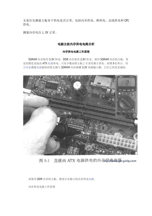
无复位先测量主板各个供电是否正常,包括内存供电、桥供电、总线供电和CPU 供电。
测量内存电压1.8V正常。
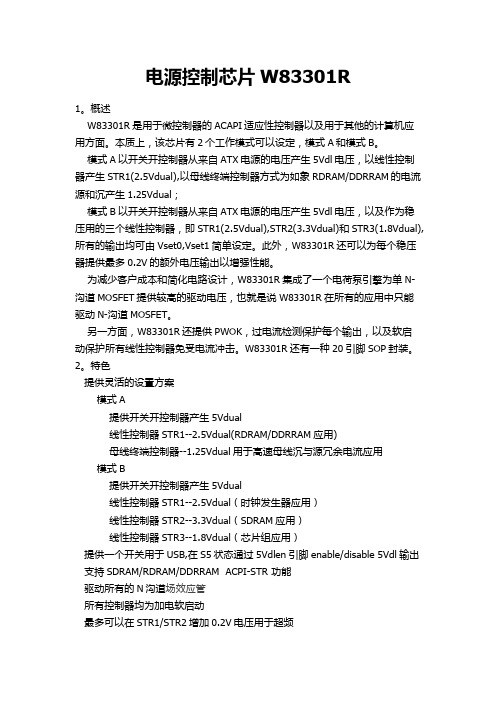
电脑主板内存供电电路分析内存供电电路工作原理SDRAM内存使用3.3V供电,DDR内存使用2.5V供电。
使用SDRAM内存的主板,常见的都是直接由ATX电源供电,只有少数高档主板上才采用独立供电。
如图5-1所示,用万用表测量电源插座的第1脚与SDRAM内存插槽3.3V电源输入脚,它们之间是直通的。
而使用DDR内存的主板,都设计有独立的内存供电电路。
内存供电电路工作原理内存供电电路人多采用集成运算放大器驱动场效应管的方式,其供电原理如图5-2所示,内存供电实际电路如图5-3所示。
图5-2内存供电电路的原理是这样的:从A点取得2.5V的基准电压进入到运算放大器的同相输入端IN+,运算放大器将IN+与IN-的电压相比较,如果IN+的电压大于IN-的电压,那么OUT的电压上升,OUT的电压上升使得Q1场效应管进一步导通,漏极(D)与源极(S)之间的管压降下降,使得B点的电压上升。
通过反馈,IN-的电压也上升,直到IN +=IN-,也就是IN+=B 。
这个过程可以简单地描述为:(IN+>IN-)→(OUT ↑)→(DS ↓)→(B ↑)→(IN-↑),直到IN+=IN-。
同理,当IN+<IN-时,它的稳压过程是这样的:(IN+<IN-)→(OUT↓)→(DS↑)→(B↓)→(IN-↓),直到IN+=IN-。
这个电路通过反馈比较,间接地控制B点的电压与基准电压相等,因此有时也称运算放大器为比较放大器。
要使B点的电压稳定,必须保证A点的电压稳定,也就是要求基准电压要稳定。
在图5-2的电路中,根据串联电路分压的原理,电阻两端的电压与其阻值的大小成正比,可以算出A点对地的电压为:3.3V×(3.24K/(IK+3.24K》≈2.5V这是使用最简单的串联分压方法取得2.5V的基准电压。
选购主板
任务3 选购主板【知识目标】熟悉主板的组成;了解主板的分类;熟悉主板的芯片组;了解目前市场的主板品牌。
【技能目标】能够识别主板的核心元器件;能够将其他各主要硬件连接到主板的相应接口能够根据需要选购合适的主板。
3.1任务描述主板是计算机的核心部件之一,其质量将影响到整台计算机运行的稳定。
在选购计算机的各配件时往往需要优先考虑主板,它也是整台计算机硬件当中最难选购的部件。
那么,用户如何在品种繁多的主板中选购合适的一款呢?3.2 相关基础知识主板安装在机箱内,是微机最基本的、也是最重要的部件之一。
主板一般为矩形电路板,分为4层板和6层板。
3.2.1 主板的组成市场上主板品牌多,布局不同,但其基本组成是一致的,主要包括CPU插槽、南北桥芯片、I/O控制芯片、内存插槽、各种电源接口、网卡芯片、声卡芯片、BIOS芯片、AGP或者PCI-E插槽、PCI插槽及各种接口(IDE和STAT接口、软驱接口、串行口、并行口、USB 接口、键盘接口、鼠标接口)等,如图3.1所示。
图3.1 主板的结构1.CPU插座或插槽主板上最醒目的接口是CPU插座(目前绝大部分是Socket接口),是用来安装CPU的接口。
CPU只有正确地安装在CPU插座(或插槽)上,才可以正常地工作。
2.控制芯片级控制芯片组是主板止尺寸最大的芯片,它一般由南桥和北桥芯片组成。
一块主板的性能是否稳定与芯片组有很大的关系,它们是主板的灵魂。
对于主板而言,芯片组几乎决定了这块主板的功能,而主板的功能又能影响到整个计算机系统的发挥,所以芯片是主板的核心或者中心。
(1)北桥芯片:通常靠近CPU插座的芯片称为北桥芯片,它主要负责CPU、内存和显卡的控制。
(2)南桥芯片:靠近PCI插槽的芯片称为南桥,它主要负责控制系统的输入、输出等设备。
南桥和北桥合成为芯片组。
这个芯片组可以随意搭配,官方规定的芯片组是由82845MCH(北桥芯片)和ICH2(南桥芯片)组成的。
Intel i845/i850及更新型的系列芯片组不再有北桥芯片和南桥芯片之分,而是用MCH和ICH代替。
BP2833-M8833替代
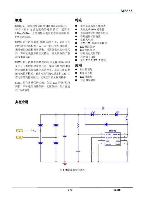
概述M8833 是一款高精度降压型LED 恒流驱动芯片。
芯片工作在电感电流临界连续模式,适用于85Vac~265Vac 全范围输入电压的非隔离降压型LED 恒流电源。
M8833 芯片内部集成 500V 功率开关,采用专利的驱动和电流检测方式,芯片的工作电流极低,无需辅助绕组检测和供电,只需要很少的外围元件,即可实现优异的恒流特性,极大的节约了系统成本和体积。
M8833 芯片内带有高精度的电流采样电路,同时采用了专利的恒流控制技术,实现高精度的 LED 恒流输出和优异的线电压调整率。
芯片工作在电感电流临界模式,输出电流不随电感量和 LED 工作电压的变化而变化,实现优异的负载调整率。
M8833 具有多重保护功能,包括 LED 开路/短路保护,SEN 电阻短路保护,欠压保护,芯片温度过热调节等。
典型应用特点⏹电感电流临界连续模式⏹内部集成500V 功率管⏹无需辅助绕组检测和供电⏹芯片超低工作电流⏹宽输入电压⏹±3% LED 输出电流精度⏹LED 开路保护⏹LED 短路保护⏹芯片供电欠压保护⏹过热调节功能⏹采用DIP-8/SOP-8 封装应用⏹LED 吸顶灯⏹LED 日光灯⏹LED 球泡灯⏹其它LED 照明图1 M8833 典型应用图定购信息管脚封装图2 管脚封装图管脚描述极限参数(注1)注 1:最大极限值是指超出该工作范围,芯片有可能损坏。
推荐工作范围是指在该范围内,器件功能正常,但并不完全保证满足个别性能指标。
电气参数定义了器件在工作范围内并且在保证特定性能指标的测试条件下的直流和交流电参数规范。
对于未给定上下限值的参数,该规范不予保证其精度,但其典型值合理反映了器件性能。
注2:温度升高最大功耗一定会减小,这也是由T JMAX, θJA,和环境温度T A 所决定的。
最大允许功耗为P DMAX = (T JMAX - T A)/ θJA或是极限范围给出的数字中比较低的那个值。
注3:人体模型,100pF 电容通过1.5KΩ电阻放电。
主板上各种芯片、元件的识别及作用
主板芯片组:芯片组(Chipset)是主板的核心组成部分,联系CPU和其他周边设备的运作。
主板上最重要的芯组就是南桥和北桥。
1、北桥芯片:(North Bridge)是主板芯片组中起主导作用的最重要的组成部分,也称为主桥(Host Bridge)。
一般来说,芯片组的名称就是以北桥芯片的名称来命名的,例如英特尔875P芯片组的北桥芯片是82875P、最新的则是支持双核心处理器的945/955/975系列的82945P、82945G、82945GZ、82945GT、82945PL、82955X、82975X等七款北桥芯片等等。
北桥作用:北桥芯片负责与CPU的联系并控制内存(仅限于Intel的cpu,AMD系列cpu 在K8系列以后就在cpu中集成了内存控制器,因此AMD平台的北桥芯片不控制内存)、AGP数据在北桥内部传输,提供对CPU的类型和主频、系统的前端总线频率、内存的类型(SDRAM,DDR SDRAM 以及RDRAM等等)和最大容量、AGP插槽、ECC纠错等支持,整合型芯片组的北桥芯片还集成了显示核心。
北桥识别及特点:北桥芯片就是主板上离CPU最近的芯片,这主要是考虑到北桥芯片与处理器之间的通信最密切,为了提高通信性能而缩短传输距离。
因为北桥芯片的数据处理量非常大,发热量也越来越大,所以现在的北桥芯片都覆盖着散热片用来加强北桥芯片的散热,有些主板的北桥芯片还会配合风扇进行散热。
因为北桥芯片的主要功能是控制内存,而内存标准与处理器一样变化比较频繁,所以不同芯片组中北桥芯片是肯定不同的,当然这并不是说所采用的内存技术就完全不一样,而是不同的芯片组北桥芯片间肯定在一些地方有差别。
2、南桥芯片:南桥芯片(South Bridge)是主板芯片组的重要组成部分,一般位于主板上离CPU插槽较远的下方,PCI插槽的附近,这种布局是考虑到它所连接的I/O总线较多,离处理器远一点有利于布线。
相对于北桥芯片来说,其数据处理量并不算大,所以南桥芯片一般都没有覆盖散热片。
内存电路详解
SDRAM内存使用3.3V供电,DDR内存使用2.5V供电。
使用SDRAM内存的主板,常见的都是直接由AT*电源供电,只有少数高档主板上才采用独立供电。
如图5-1所示,用万用表测量电源插座的第1脚与SDRAM内存插槽3.3V电源输入脚,它们之间是直通的。
而使用DDR内存的主板,都设计有独立的内存供电电路。
内存供电电路工作原理内存供电电路人多采用集成运算放大器驱动场效应管的方式,其供电原理如图5-2所示,内存供电实际电路如图5-3所示。
图5-2内存供电电路的原理是这样的:从A点取得2.5V的基准电压进入到运算放大器的同相输入端IN+,运算放大器将IN+与IN-的电压相比拟,如果IN+的电压大于IN-的电压,则OUT的电压上升,OUT的电压上升使得Q1场效应管进一步导通,漏极〔D〕与源极〔S〕之间的管压降下降,使得B点的电压上升。
通过反应,IN-的电压也上升,直到IN+=IN-,也就是IN+=B 。
这个过程可以简单地描述为:〔IN+>IN-〕→〔OUT ↑〕→〔DS ↓〕→〔B ↑〕→〔IN-↑〕,直到IN+=IN-。
同理,当IN+<IN-时,它的稳压过程是这样的:〔IN+<IN-〕→〔OUT↓〕→〔DS↑〕→〔B↓〕→〔IN-↓〕,直到IN+=IN-。
这个电路通过反应比拟,间接地控制B点的电压与基准电压相等,因此有时也称运算放大器为比拟放大器。
要使B点的电压稳定,必须保证A点的电压稳定,也就是要求基准电压要稳定。
在图5-2的电路中,根据串联电路分压的原理,电阻两端的电压与其阻值的大小成正比,可以算出A点对地的电压为:3.3V×〔3.24K/〔IK+3.24K"≈2.5V这是使用最简单的串联分压方法取得2.5V的基准电压。
这种串联分压电路的缺点是当3.3V的电压波动时,基准电压也会跟着波动,所以有的内存供电电路使用TL431〔三端可调分流式电压基准源〕来提供基准电压,如图5-4所示。
电源控制芯片W83301R
电源控制芯片W83301R1。
概述W83301R是用于微控制器的ACAPI适应性控制器以及用于其他的计算机应用方面。
本质上,该芯片有2个工作模式可以设定,模式A和模式B。
模式A以开关开控制器从来自ATX电源的电压产生5Vdl电压,以线性控制器产生STR1(2.5Vdual),以母线终端控制器方式为如象RDRAM/DDRRAM的电流源和沉产生1.25Vdual;模式B以开关开控制器从来自ATX电源的电压产生5Vdl电压,以及作为稳压用的三个线性控制器,即STR1(2.5Vdual),STR2(3.3Vdual)和STR3(1.8Vdual),所有的输出均可由Vset0,Vset1简单设定。
此外,W83301R还可以为每个稳压器提供最多0.2V的额外电压输出以增强性能。
为减少客户成本和简化电路设计,W83301R集成了一个电荷泵引擎为单N-沟道MOSFET提供较高的驱动电压,也就是说W83301R在所有的应用中只能驱动N-沟道MOSFET。
另一方面,W83301R还提供PWOK,过电流检测保护每个输出,以及软启动保护所有线性控制器免受电流冲击。
W83301R还有一种20引脚SOP封装。
2。
特色提供灵活的设置方案模式A提供开关开控制器产生5Vdual线性控制器STR1--2.5Vdual(RDRAM/DDRRAM应用)母线终端控制器--1.25Vdual用于高速母线沉与源冗余电流应用模式B提供开关开控制器产生5Vdual线性控制器STR1--2.5Vdual(时钟发生器应用)线性控制器STR2--3.3Vdual(SDRAM应用)线性控制器STR3--1.8Vdual(芯片组应用)提供一个开关用于USB,在S5状态通过5Vdlen引脚enable/disable 5Vdl输出支持SDRAM/RDRAM/DDRRAM ACPI-STR 功能驱动所有的N沟道场效应管所有控制器均为加电软启动最多可以在STR1/STR2增加0.2V电压用于超频低电压失效监察软启动功能20脚SOP封装7.功能描述7。
主板常见故障
主板常见故障解决办法2007-07-26 18:10一、开机无显示由于主板原因,出现此类故障一般是因为主板损坏或被CIH病毒破坏BIOS造成。
一般BIOS被病毒破坏后硬盘里的数据将全部丢失,是以我们可以通过检测硬盘数据是否完好来判断BIOS是否被破坏,还有两种原因会造成该现象:1、因为主板扩展槽或扩展卡有问题,导致插上诸如声卡等扩展卡后主板没有响应而无显示。
2、对于现在的免跳线主板而言,如若在CMOS里设置的CPU频率不对,也可能会引发不显示故障,对此,只要清除CMOS即可予以解决。
清除CMOS的跳线一般在主板的锂电池附近,其默认位置一般为1、2短路,只要将其改跳为2、3短路几秒种即可解决问题,对于以前的老主板如若用户找不到该跳线,只要将电池取下,待开机显示进入CMOS设置后再关机,将电池上上去亦达到CMOS放电之目的。
对于主板BIOS被破坏的故障,我们可以插上ISA显卡看有无显示,倘若没有开机画面,也可以自己做一张自动更新BIOS的软盘,重新刷新BIOS,但有的主板BIOS被破坏后,软驱根本就不工作(据我所知,承启的主板就是这样),此时,可尝试用热插拔法解决,但据我个人经验,采用热插拔除需要相同的BIOS外还可能会导致主板部分元件损坏,所以可靠的方法是用写码器将BIOS更新文件写入BIOS里面(维修手机的地方一般都有写码器)。
对于主板损坏的故障,有的可能是因为主板用久后电池漏液导致电路板发霉(针对以前的老主板而言),使得主板无法正常工作,对此我们可以对其进行彻底清洗看能否解决问题,此方法还对主板各插槽的接触不良有治根之妙。
清洗方法:用工具拔掉主板上的BIOS、CMOS电池,然后用硬毛刷、洗衣粉,对其各部件进行彻底清洗,最后用自来水冲洗干净,待主板阴干后再试(笔者曾用此法治好过几块主板,且没有发现任何后遗症)。
二、主板COM口或并行口、IDE口损坏出现此类故障一般是由于用户带电插拔相关硬件造成,此时用户可以用多功能卡代替,但在代替之前必须先禁止主板上自带的COM口与并行口(有的主板连IDE 口都要禁止方能正常使用)。
- 1、下载文档前请自行甄别文档内容的完整性,平台不提供额外的编辑、内容补充、找答案等附加服务。
- 2、"仅部分预览"的文档,不可在线预览部分如存在完整性等问题,可反馈申请退款(可完整预览的文档不适用该条件!)。
- 3、如文档侵犯您的权益,请联系客服反馈,我们会尽快为您处理(人工客服工作时间:9:00-18:30)。
WinbondACPI-STR ControllerW83301RDate: 2002/07 Revision: 1.0W83301RData Sheet Revision HistoryPages Dates Version Versionon WebMain Contents1 07/2002 1.0 1.0 1st ReleasePlease note that all data and specifications are subject to change without notice. All the trademarks of products and companies mentioned in this datasheet belong to their respective owners.LIFE SUPPORT APPLICATIONSThese products are not designed for use in life support appliances, devices, or systems where malfunction of these products can reasonably be expected to result in personal injury. Winbond customers using or selling these products for use in such applications do so at their own risk and agree to fully indemnify Winbond for any damages resulting from such improper use or sales.The W83301R is an ACPI-compliant controller for microprocessor and other computer applications. In substance, the part can mainly operate in alternative configurations mode A and B – mode A provides a switch controller to generate a 5V DL voltage from ATX power supply, a linear controller – STR1 (2.5V DUAL), and a bus termination controller – 1.25 V DUAL for high speed bus such as RDRAM/DDRAM current sinking and sourcing; and mode B provides a switch controller to generate a 5V DL voltage from ATX power supply and three linear controllers for specific voltage regulations – that is STR1 (2.5V DUAL), STR2 (3.3V DUAL) and STR3 (1.8 V DUAL), all of the outputs can simply configured by V SET0, V SET1. Besides, the W83301R also can provide extra voltage up to 0.2V in each regulator output for more performance. In order to reduce the customer’s cost, and simplify the circuit design, the W83301R integrates a charge-pump engine into the chip to provide higher driving voltage for single N-channel MOSFETs, that is the W83301R, can drive only N-channel MOSFETs for all applications. In the other hand, the W83301R also offer PWOK and over current detection to protect each output and soft-start protects all linear controllers from rush current attack. The W83301R is available in a 20-pin SOP package.2. FeaturesProvides alternative configurations for flexible applicationsMode AProvide a switch controller to generate 5V DUALLinear controller STR1–2.5V DUAL (RDRAM/DDRAM application)Bus termination controller –1.25V DUAL for high speed bus termination application to sinking and sourcing redundant currentMode BProvide a switch controller to generate 5V DUALLinear controller STR1 – 2.5V DUAL (Clock Gen. Application)Linear controller STR2 – 3.3 V DUAL (SDRAM Application)Linear controller STR3 – 1.8V DUAL (Chipset Application)Provide a switch to enable/disable 5V DL output in S5 state via 5V DLEN pin for USB applicationSupports SDRAM/RDRAM/DDRAM ACPI-STR FunctionsDrives all N-Channel MOSFETsPower-Up Softstart for all controllersUp to 0.2V incremental voltage on STR1/STR2 for over-clock application.Under-Voltage Fault MonitorSoft-Start function20-Pin SOP Packageinbond W83301RSYMBOL PIN FUNCTIONMode A: BT Current Source. Connect this pin to the gate of a suitable N-channel MOSFET for driving bus termination regulator output.STR DRV2/BT DRV 1Mode B: STR2 Driver. Connect this pin to the gate of a suitable N-channel MOSFET for driving STR2 output.Mode A: BT Sense. Connect this pin to the bus termination regulator output.STR SEN2/BT SEN 2Mode B: STR2 Sense. Connect this pin to the STR2 output.Mode A: BT Current Sink. This pin is used to drive a N-channel MOSFET to sink the redundant current in the high-speed bus.STR DRV3/BT SINK 3Mode B: STR3 Driver. Connect this pin to the gate of a suitable N-channel MOSFET for driving STR3 output.Mode A: Function Reserved. Pull up this pin to +5VSB through a 1.5 Kohm resistor. STR SEN3 4Mode B: STR3 Sense. Connect this pin to the STR3 output.GND 5 Power Ground. Connect this pin to ground. Vcc 6 Power Vcc. Input 5VSB supply.C1 7Charge Pump Cap. Attach flying capacitor between this pin and C2 to generateinternally used high voltage from 5V power supply.C2 8Charge Pump Cap. Attach flying capacitor between this pin and C1 to generateinternally used high voltage from 5V power supply.ChrPmp 9Charge Pump output. This pin produces voltage doubled 5V supply by charge-pumping. Bypass with a 0.1uF capacitor.5V DLEN # 10 5VDL Enable. Control 5V DL voltage output. Pull-up internally. S5# 11 S5 Status. Control signal governing the soft off state S5. Pull-up internally. S3# 12 S3 Status. Control signal governing the soft off state S3. Pull-up internally.V SET1 13Voltage Selection 1. Combine with VSET2 to select operation mode and outputvoltages of STR regulators.V SET0 14Voltage Selection 0. Combine with VSET1 to select operation mode and outputvoltages of STR regulators.5V DLSB 155VSB Output Control. Connect this pin to the gate of a N-MOSFET to output5VSB power to 5V DL .5V DRV 165V Output Control. Connect this pin to the gate of a N-MOSFET to output 5Vpower to 5V DL .PWOK 17 Power OK. Open collector input/output. Used to indicate the ready of 5Vin supply. Ifany STR supply (only STR1 in mode A) occurs over current and induce under-voltage, PWOK will be pull down.SS 18Soft-Start. Attach a capacitor (0.033u) to this pin to determine the softstart rate. A ramp generated by charging this capacitor with internal soft-start current (18uA) isused to clamp the voltage rising slew rate of STR regulators and 5V DL . Soft starting avoids too much rush current during voltage setup.STR SEN1 19 STR1 Sense. Connect this pin to the STR1 output.STR DRV1 20STR1 Driver. Connect this pin to the gate of a suitable N-channel MOSFET fordriving STR1 output.Figure 2. Mode A (DDR Mode) Application CircuitMode VSET0 VSET1 STR1Bus Termination Controller0V 0V 2.5V DUAL 1.25V DUAL0V NC 2.6V DUAL 1.30V DUAL DDR0V 5V 2.7V DUAL 1.35V DUAL5VDUAL(chipset)5. Application CircuitFigure 3. Mode B (SDRAM Mode) Application Circuit5VDUAL(chipset)Mode VSET0 VSET1 STR1 STR2 STR3 5V 5V2.5V DUAL3.3V DUAL 1.8V DUALSDRAM2.6V DUAL3.4V DUAL 1.8V DUAL5V NC2.7V DUAL3.5V DUAL 1.8V DUAL5V 0V6.Block DiagramFigure 4. W83301R Internal Block DiagramS3S5VSET0 VSET1 SS 5V DLSB 5V DRV 5V DLEN # STR DRV1/BT DRVSTR SEN1/BT SENSTR DRV2/BT SINK STR SEN2STR DRV3 GND STR SEN37. Functional Description7.1 Mode SelectionThe W83301R supports two modes for customer’s multi-applications, as shown as Table1, the mode A and mode B can selected via VSET0 pin. If this pin connects to 5V, the chip will operate under mode A, otherwise the chip will operate under mode B when VSET0 connects to ground.Both mode A and B supports a linear switch to generate an ACPI-compliant 5V DL voltage from ATX power supply 5V/5V SB according to S5# and S3# signals. And user also can turn off the whole 5V DL output in S5 state via 5V DLEN# pin if needed.Under the mode A operation, the chip provide a linear controller STR1 that drives a N-channel MOSFET Q3 (refer to figure) to generate a regulated voltage 2.5V DUAL from an external power source 3.3V DUAL, the 2.5 V DUAL is provide for RDRAM/DDRAM ACPI suspend to RAM application. And In order to simply the circuit design and reduce customer’s cost, the W83301R also integrate a bus termination controller BT driving two external N-channel MOSFETs (Q4, Q5) to generate a specific ACPI-compliant voltage according to a half of STR1 output for sourcing and sinking bus redundant current.Under the mode B operation, the chip provide three linear controllers, that is STR1- 2.5V DUAL, STR2- 3.3 V DUAL, and STR3- 1.8V DUAL, all of the three outputs drive a N-channel MOSFET (Q3, Q4, and Q5) to generate an ACPI-compliant voltage by different applications. Such as STR1- 2.5V DUAL for clock generator application, STR2- 3.3 V DUAL for SDRAM application, and STR3- 1.8V DUAL chipset application.Besides, as shown in Table 1 the W83301R also provide a tri-state pin VSET1 to bias an extra voltage up to 0.2V in each output for more performance but under mode A operation, the BT output voltage will generated according to a half of STR1 output set by VSET1.Table 1. W83301R Control TableMode VSET0 VSET1 STR1 Bus Termination Controller Remark0V 0V 2.5V DUAL 1.25V DUAL0V NC 2.6V DUAL 1.30V DUAL A0V 5V 2.7V DUAL 1.35V DUAL -STR1 output for RDRAM/DDRAM voltage -Bus Termination Controller for memory bus redundant current sinking and sourcing.Mode VSET0 VSET1 STR1 STR2 STR3 Remark5V 5V 2.5V DUAL 3.3V DUAL 1.8V DUAL5V NC 2.6V DUAL 3.4V DUAL 1.8V DUAL B5V 0V 2.7V DUAL 3.5V DUAL 1.8V DUAL -STR1 output for Clock Gen. voltage -STR2 output for SDRAM voltage-STR3 output for Chipset voltage7.2 ACPI State ControlIn order to meet the ACPI specification, the W83301R implement a state machine as shown as Figure 5 to generate ACPI-compliant power state transition.There are only five states in the state machine cause the W83301R only focus on the memory ACPI control, and the five states are G3 (Mechanical-Off State), S0 (Full-Power State), S3 (Sleeping State-Suspend to RAM), S5On (Soft-Off State), S5Off and all of these states changed to the other according to the condition of S3#, S5# and 5V DLEN #. On the other hand, cause of the W83301R allows customer to disable/enable the 5V DUAL output in S5 state via 5V DLEN # pin, there are two states, S5On and S5Off , corresponding to S5 state. A soft ramp-up mechanism is needed to protect the 5V DL output from the rush current attack during the S5Off to S5On state transition. Same as the 5V DL output, the W83301R also provides soft ramp-up mechanism during S5On to S0 state transition in each STR output.In the state machine, when the power on, and the 5V input from power supply arrive 4.5V, the chip will enter S5Off first from G3, and ramp-up into S5On state by two conditions, the one is when 5V DLEN #=0 under standby power supply to resume the 5V DL output, the other one is S3#=1 and S5#=1 the system will enter S1 state.During S5On state, the chip will return back to S5Off when the customer wants disabling the 5V SB output (5V DLEN #=1) to save some power. And the chip will drive all outputs into S0 state will S3#=1 and S5#=1.When the system under the S0 state, the system should enter the S3-sleeping (S3#=0, S5#=1) or S5-soft off (S5#=0) state when the system idle for a long time or user power-off.When the system suspend to RAM, the system will be wakeup and enter S0-full power state by (S3#=1, S5#=1,PWOK=1), or get into S5-sleeping soft off state by (S5#=0)Table 2. W83301R Outputs TableState 5V DL STR1 STR2 STR3 LUV Activity * G3 Off Off Off Off No S5 (5V DL Off) Off Off Off Off NoS5 (5V DL On) On(Driven by 5V DLSB ) Off Off Off NoS0 On(Driven by 5V DRV ) On On On YesS3 On(Driven by 5V DLSB )On On On Yes*When the STR2 & STR3 configured as bus termination controller, only STR1 has linear under voltage function.7.3 Charge PumpIn order to simply the design circuit and provide a good-price solution for customer, the W83301R integrate with a switched-capacitor voltage doubler charge pump to provide a higher driving voltage (Up to 10 volt) and can drive a single N-channel MOSFETs in each output.7.4 Power OKThe W83301R use a bi-direction Power OK signal to ensure the system can work normally. When the system jump from state S3 to state S0, the W83301R will monitor the input signal from PWOK pin to ensure that external system power is OK and then switch each outputs into S0 stage; In the other hand, the W83301R will pull down the Power OK signal to inform the system that a over current and induce under-voltage occurred.7.5 Soft-StartDuring ‘S5off’ to ‘S5on’ and ‘S5on’ to ‘S0’ state transitions, the 5Vdual and STR voltages need to ramp up from 0 to their set values respectively. The charging current flowing to output capacitors must be limited to avoid supply drop-off.In W83301R, an internal 18 uA current source (Iss) charges an external capacitor (Css) to generate a linear ramp-up voltage on SS pin (Vss). The Vss slews from 0 to about 9V during the above-mentioned state transitions, and the Vss slew rate is used to clamp the ramp-up rate of 5Vdual and STR output voltages. This output clamping allows power-ups free of supply drop-off events.Since the outputs are ramped up in a constant slew-rate, the current dedicated to charge any output capacitor can be calculated with the following formula:I COUT = Iss x (Cout / Css)Some technique is included in W83301R to further reduce the total charging current: In Mode B configuration, the start-up of ramp-up time STR3 (1.8V) will be advanced from that of STR1 to reduce the overlap time of charging. And in Mode A configuration, the bus-terminator is input clamped, and its output voltage slew-rate, so as its charging current, will be limited to half of that of STR1.Note that, too slow ramp-up rate is not recommended. If so, the state transition mentioned above will be prolonged to much. Before Vss ramps up to its upper limit (about 9V), the state transition will not be completed and will not go into next state.8.1 ABSOLUTE MAXIMUM RATINGSStresses greater than those listed in this table may cause permanent damage to thedevice. Precautions should be taken to avoid application of any voltage higher than themaximum rated voltages to this circuit. Subjection to maximum conditions for extendedperiods may affect reliability. Unused inputs must always be tied to an appropriate logicvoltage level (Ground or Vdd).Symbol Parameter Rating Vss, V cc Voltage on any pin with respect to GND - 0.5 V to + 7.0 VChrPmp - 0.5 V to + 12.0 VHi-V Pins Pin# 1,2,3,4,8,15,16,18,19,20 GND-0.3 V to V Chr-Pmp + 0.3VLo-V Pins Pin# 7,10,11,12,13,14,17 GND-0.3 V to Vcc + 0.3VT STG Storage Temperature - 65°C to + 150°CT B Ambient Temperature - 55°C to + 125°CT A Operating Temperature 0°C to + 70°C8.2 AC CHARACTERISTICSVcc=5V ± 5 %, T A = 0°C to +70°CTestUnitsConditions Parameter SymbolMaxMinTypVcc SUPPLY CURRENTNorminal Supply Current I5VSB 6 mAPOWER-ON RESETRising V5VSB Threshold 4.3 V V Chr_Pmp > 8.5V5VSBHysteresis 1 VRising V Chr_Pmp Threshold 8.5 V V5VSB > 4.3VV Chr_Pmp Hysteresis 1 VSOFT-STARTSoft-Start Current Iss 18 uAV SS upper limit 9 V8.2 AC CHARACTERISTICS (Continued)Vcc=5V ± 5 %, T A = 0°C to +70°CParameter Symbol Min Typ Max Units Test ConditionsSTR1 lINEAR REGULATOR Nominal Output Voltage2.5 V VSET0=0V, VSET1=0V or VSET0=5V,VSET1=5VNominal Output Voltage2.6 V VSET0=0V, VSET1=NC or VSET0=5V,VSET1=NCNominal Output Voltage 2.8 V VSET0=0V, VSET1=5Vor VSET0=5V,VSET1=0VRegulation 5 % STR SEN1 Under-Voltage Falling Threshold 80 % MAX STR DRV1 Output Voltage6 V I(STR DRV1) < 0.1mASTR2 LINEAR REGULATORNominal Output Voltage 3.3 V VSET0=5V,VSET1=5V Nominal Output Voltage 3.4 V VSET0=5V,VSET1=NC Nominal Output Voltage 3.5 V VSET0=5V,VSET1=0VRegulation 5 %STR SEN1 Under-Voltage Falling Threshold80 % MAX STR DRV1 Output Voltage6 V I(STR DRV1) < 0.1mA STR3 LINEAR REGULATORNominal Output Voltage1.8 V VSET0=5V Regulation 5 % STR SEN1 Under-Voltage Falling Threshold83 % MAX STR DRV1 Output Voltage6 V I(STR DRV1) < 0.1mA BUS TERMINATORNominal Output Voltage / V STRSEN150 % VSET0=0V Regulation 5 %5VDUAL SWITCH CONTROLLER5V DRV Output High Voltage 9 Cload=3000p 5V DRV Sourcing Current 7 mA Cload=3000p 5V DRV Sinking Current 400 uA Cload=3000p 5V DLSB Output High Voltage 9 Cload=3000p 5V DLSB Sourcing Current 7 mA Cload=3000p 5V DLSB Sinking Current 230 uA Cload=3000p S3#,S5#,5VDLEN#, PWOK,CHARGE PUMP Input Logic High 2.2 V9. Package Specification 20L SSOP-209 mil10. Ordering InformationPart Number Package Type Production Flow W83301R20-PIN SSOPCommercial, 0°C to +70°C11. How to Read the Top MarkingLeft Line: Winbond Logo 1st line: Part No W83301R-G2nd line: Tracking code XXXXXXXXX3rd line: Package date code XXX + assembly house ID X + B: the IC version 1: wafers manufactured in Winbond FAB I1039050-21NA: wafer production series numberHeadquartersNo. 4, Creation Rd. IIIScience-Based Industrial Park Hsinchu, Taiwan TEL: 886-35-770066FAX: 886-35-789467www: /Taipei Office11F, No. 115, Sec. 3, Min-Sheng East Rd.Taipei, TaiwanTEL: 886-2-7190505FAX: 886-2-7197502TLX: 16485 WINTPEWinbond Electronics (H.K.) Ltd.Rm. 803, World Trade Square, Tower II 123 Hoi Bun Rd., Kwun Tong Kowloon, Hong Kong TEL: 852-********-7FAX: 852-********Winbond Electronics (North America) Corp.2730 Orchard Parkway San Jose, CA 95134 U.S.A.TEL: 1-408-9436666FAX: 1-408-9436668Please note that all data and specifications are subject to change without notice. All the trade marks of products and companies mentioned in this data sheet belong to their respective owners. These products are not designed for use in life support appliances, devices, or systems where malfunction of these products can reasonably be expected to result in personal injury. Winbond customers using or selling these products for use in such applications do so at their own risk and agree to fully indemnify Winbond for any damages resulting from such improper use or sale.W83301R-G 114984302 302GBNA。