CM2596中文资料
XL2596 DEMO 板手册说明书

页数:第1 页,共3 页描述221016A02是为产品XL2596制作的演示板,用于DC8V~40V输入,输出电压5V,输出电流3A的降压恒压应用演示,最高转换效率可以达到85%。
XL2596是开关降压型DC-DC转换芯片;固定开关频率150KHz,可减小外部元器件尺寸,方便EMC设计。
芯片具有出色的线性调整率与负载调整率,输出电压支持1.23V~37V间任意调节。
芯片内部集成过流保护、过温保护、短路保护等可靠性模块。
XL2596为标准TO263-5L封装,集成度高,外围器件少,应用灵活。
DEMO原理图引脚介绍页 数:第 2 页, 共 3 页物料清单序号 数量 参考位号 说明生产商型号 生产商 1 2 C1,C2 1uF,50V,Ceramic,X7R,0805 C2012X7R1H105K TDK 2 1 CFF 33nF,50V,Ceramic,X7R,0603 C1608X7R1H333K TDK 3 2 CIN, COUT220uF,50V,Electrolytic,(10*16) YXJ-50V-220uFRubycon 4 1 D1 60V,5A,SMC,Schottky Barrier RectifierB560CDIODES5 1 L1 100uH,4A,(18*9)6 1 R1 14K Ω,1%,1/16W,Thick Film,0603 RC0603FR-0714KL Yageo7 1 R2 43K Ω,1%,1/16W,Thick Film,0603RC0603FR-0743KLYageo 81U140V,3A,BUCK,DC-DC Converter,TO263-5LXL2596XLSEMIDEMO 实物图PCB 布局40mm顶层 底层30mm页数:第3 页,共3 页应用信息输入电容选择在连续模式中,转换器的输入电流是一组占空比约为VOUT/VIN的方波。
为了防止大的瞬态电压,必须采用针对最大RMS电流要求而选择低ESR(等效串联电阻)输入电容器。
LM2596中文资料
LM2596S-3.3, LM2596S-5.0,LM2596S-12, LM2596S-ADJ为TO-263封装(SMT)。
η
效率
VIN=12V,ILOAD=3A
73
LM2596□—5.0 (见注 14)
VOUT
输出电压
5.0 7V≤VIN≤40V, 0.2A≤ILOAD≤3A
η
效率
VIN=12V,ILOAD=3A
80
3.168/3.135 3.432/3.465
V V(min) V(max) %
4.800/4.750 5.200/5.250
2 30
A A(min) A(max) μA(max) mA mA(max)
IQ
静电流
见注 9
5 10
mA mA(max)
ISTBY
待机静电流
ON/OFF 脚=5V(OFF)(9)
80
μA
200/250
μA(max) 3
开发板精品网www.mcu361.com为您提供各种开发板和电子技术资料
LM2596 开关电压调节器 SEPTEMBER, 2004
ILOAD=500mA。 (见注 14)
361 符号
参量
cu 器件参数
.m Ib
反馈偏置电流
wwwfO
振荡器频率
条件
LM2596□—XX
典型值(2) 极限值(3)
单位
只适用于输出可调节的情况,VFB=1.3V
JR劲锐佳芯片各型号使用明细
我司强势推出大电流电源IC\电源管理IC及大小功率的充电器IC,广泛应用在DVD, DVB(机顶盒),便携式DVD,车载DVD/VCD,液晶电视,液晶显示器,路由器,车载充电器,电瓶车控制电路板,车载冰箱,汽车音响,恒流串联LED灯驱动, VOIP,Audio,LCDM及各种小家电产品.XLSEMI产品应用领域1.DVB(机顶盒):XL1513,XL1580,XL1410(12V-1.8V/3.3V/5V/1A)2.Portable DVD:XL1410(12V-5V/3.3V/1.8V/1A),XL1580/XL1583(12 V-5V/1A)3.Video:XL1509-5.0S(12V-5V/1A)4.收音机电源:XL1509-ADJ,XL2576,XL2596组合DVD带音响/台式大收音机(带机芯):XL2576,XL2596,XL1509-ADJ5. LCD TV:XL1509-5.0/3.3、XL2596-5.0、6. LCDM:XL2596-5.0(12V-5V/3A),XL2596-3.3(15寸、17寸),XL15 07-5.0(12V-5V/1.5A)7. Audio:XL2596-5.0(12V-5V/3A)8. VOIP:XL1509-3.3(12V-3.3V/2A、12V-5V/1A),XL2596-3.39. 路由器:XL1509,XL1509-3.3,XL1410,XL151310. 液晶显示器:XL1501-3.3(12V-3.3V/3A)11.32寸以上液晶电视:XL4015(24V-12V/3A、24V-5V/5A)12.电梯控制板电源:XL2576,XL259613.锂电池包(多节锂电串联),移动电源,电池组,需恒压恒流充电:XL4001,XL4101,XL4015+358大功率锂电池包供电:XL6019,,XL6008,XL6007替代FP5138+MOS14.笔记本串联锂电池升压:XL6019,XL6008(12V~16V转19V/3A)15.车载MP3,MP4:XL1509,XL4001,XL1513(12V-5V/1 A)车载GPS:XL2596,XL150916.车载DVD:XL1507(12V-5V/1.5A,24V-5V/1.5A),XL1583(12V-5V/1.5A)17.公交车,出租车LED点阵显示屏:XL2576(24~36V转5V/1A)18.车载冰箱,汽车音响:XL4016(24V-12V/8A)19.车载充电器;XL1583,XL1410(12V~24V转5V/2A)XL4001,XL2001(12V~36V转5V/1.8A)XL4201,XL4101,XL2011,XL2012(12V~36V转5V/2.1A)XL4501,XL2013,(12V~36V转5V/3.1A~4.4A)XL1509(12V~36V转5V/1.5A),XL2576P(12V~36V转5V/1.5A),XL2576(12V~36V转5V/2A),XL2596(12V~36V转5V/2A),XL4013(12~24V转5V/3A),XL4015(12~24V转5V/4A),XL2001(12~24V转5V/1.8A),XL2011(12~24V转5V/2.1A),XL2012(12~24V转5V/2.4A),XL2013(12~24V转5V/3.2A),车充产品可以替代GL2576,GL2596,AX3007,AX3111,ACT4515,ACT4070,49 4+MOS,7500+MOS等方案20.上网本,笔记本车载充电器:60W以下的应用XL6009,XL6010,XL6011替代FP5138+MOS的方案,优点:线路简单,可靠性高升压方案(输入:10V~14V,输出:16V/19V,输出电流:2A,3A)升降压方案(输入:10V~30V,输出:12V/19V,输出电流:2A,3A)21.MR16射灯:XL30023*1W,4*1W ,5*1WLED模组驱动AC12V(DC10~16V)电子变压器升压供电:XL6003 5~7*1W,XL6005 10*1W车顶灯恒压输出,降压结构:XL1509车顶灯恒压输出,升压结构:XL6007,XL6008车顶灯恒压输出,升降压结构:XL6007,XL6008舞台灯XL2576,XL150922.电瓶车控制电路板:XL7001(60V转12V/5V/0.5A)23.安防产品:车载摄像头(小摄像头)供电:XL1509,XL1513小区,马路,建筑用的大摄像头,高速球供电:XL2596,XL1501摄像头里面用红外的LED灯驱动:XL1513,XL1530,XL1410市电和蓄电池混合供电:需要升降压应用XL6007,XL6008小区,大厦可视门铃对讲4寸,7寸屏供电:XL1509-ADJ,XL1410,XL1513,XL15 83(12V转5V/500mA)指示灯板:XL1513,XL141024.液晶电视数字屏,解码板电源驱动板:XL1513,XL153025.太阳能路灯,路标灯,庭院灯和5V~32V低压供电LED驱动,升降压应用领域:XL6003,XL6004,XL600526.大功率车载电源,降压,限流:XL4003+358,XL4005+358,XL4012+35827.降压型应用:XL4003,XL4005,XL4012可以替代PWM IC+MOS管等类似方案升压型应用:XL6007,XL6009,XL6010可以替代PWM IC+MOS管等类似方案升降压型应用:SEPIC BUCK-BOOST结构XL6007,XL6009,XL6010可以替代P WM IC+MOS管类似方案28.DVB:XL6007,XL6008马达天线供电(12V BOOST 19V/800mA)可以替代PWM IC+MOS管类似方案 CCD/CATVPMP/DSC/DSV/STB/VGA CardDPF(数码相框)PDALE D Panel背光LCD Panel背光移动电源应急充电器,可以替代FP5210+MOS,FP6210升压应用领域29.升压,恒压LED模组驱动:XL6007,XL6008,可以替代FP5210+MOS,FP621 0升压应用领域30.17寸以下LED背光驱动:XL6007,可以替代AMC3202的应用领域[1]XL14102APWM降压DC/DC,SOP8,输入3.6-18V,输出1.22V-16V转换效率高达90%,可替代BM1410A,TD1410,AP1512,AP1513,RM1410,GT1510,EC94 10,EC9410C,SD46520,ACT4060功能兼容AOZ1010AI,AOZ1015AI,EC9406[2]XL15833APWM降压DC/DC,SOP8,输入3.6-20V,输出1.23V-18V转换效率高达90%,可替代MP2355,ACT4060,MP1583,ZA3020,AOZ1014,MP1593[3]XL15132APWM降压DC/DC,SOP8,输入3.6-18V,输出0.8V-16V转换效率高达90%,可替代AP1513,OCP2020,BM1513/A,AX3101,RM2060,CX1513,EC9 413,AP1510,AP1520,AP1533,AP1534,AP5002功能兼容AOZ1010AI,AOZ1015AI,EC9406[4]XL15303APWM降压DC/DC,SOP8,输入3.6-18V,输出0.8V-16V转换效率高达90%,可替代AP1530,AP1538,AP1539,[5]XL25763APWM降压DC/DC,TO263/TO220,输入电压范围3.6-45V,可完全替换AE2576,BM2576,TD2576,AP1512/A,LM2576,LM2576,MIK2575,MIK2576A MC2576,OCP2006,HWD2575,EC942576[6]XL25963APWM降压DC/DC,TO263/TO220,输入电压范围3.6-45V,可完全替换AE2596,BM2596,TD2596,AP1501/A,AP1506,LM2596,AMC2596,MIK2596,OCP2011,OCP2016,GT1500,GT1504,AX2596,EC9401,CM2596S[7]XL15092APWM降压DC/DC,SOP8,输入3.6-36V,转换效率高达90%,功能替换LM2594,AE1509,TD1509,AP1509,OCP2019,HWD61410,EC9409,CM25 93.[8]XL4001,XL4101,XL4201,XL4501车载充电器,点烟器,恒流LED驱动,专用芯片150K2A/3A外部可调限流PWM降压DC/DC输入4.6V-40V可替代2576+431+324方案,34063+MOS+431+324方案[9]XL15073APWM降压DC/DC,TO252,输入3.6-36V,转换效率高达85%可完全替换AE1507,TD1507,AP1507,OCP2017,EC9407[10]XL4015大电流5APWM降压DC/DC,输入8-36V,输出0.8V-33V转换效率高达95%(功能兼容)---AOZ1014,LM2677,LM2678,LM2679[11]XL4012大电流12APWM降压DC/DC,TO220输入8-40V,输出0.8V-33V转换效率高达95%(功能兼容)---LM2677,LM2678,LM2679。
LM2596全中文资料
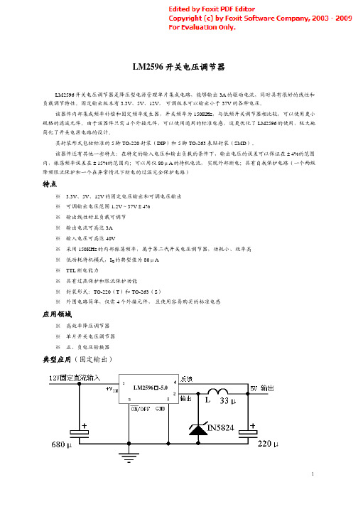
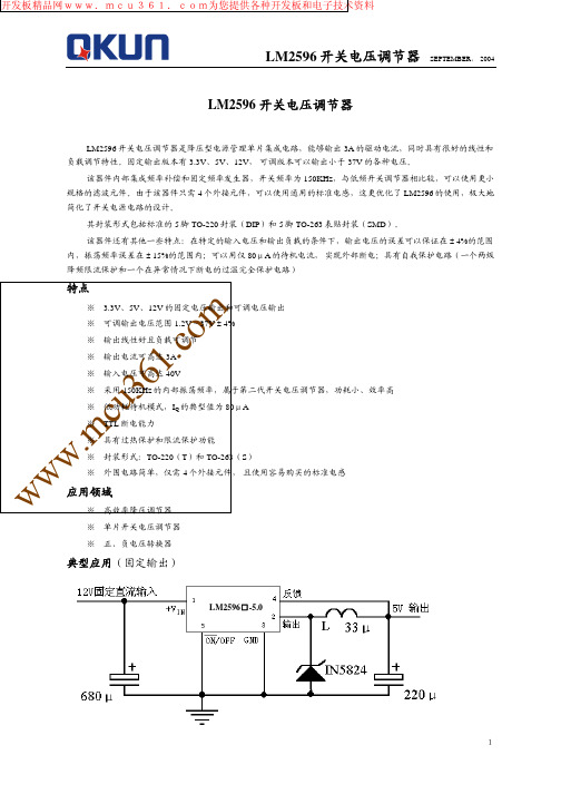
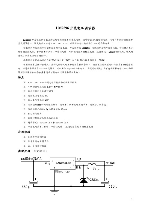
LM2596 开关电压调节器LM2596开关电压调节器是降压型电源管理单片集成电路,能够输出3A的驱动电流,同时具有很好的线性和负载调节特性。
固定输出版本有3.3V、5V、12V,可调版本可以输出小于37V的各种电压。
该器件内部集成频率补偿和固定频率发生器,开关频率为150KHz,与低频开关调节器相比较,可以使用更小规格的滤波元件。
由于该器件只需4个外接元件,可以使用通用的标准电感,这更优化了LM2596的使用,极大地简化了开关电源电路的设计。
其封装形式包括标准的5脚TO-220封装(DIP)和5脚TO-263表贴封装(SMD)。
该器件还有其他一些特点:在特定的输入电压和输出负载的条件下,输出电压的误差可以保证在±4%的范围内,振荡频率误差在±15%的范围内;可以用仅80μA的待机电流,实现外部断电;具有自我保护电路(一个两级降频限流保护和一个在异常情况下断电的过温完全保护电路)特点※ 3.3V、5V、12V的固定电压输出和可调电压输出※可调输出电压范围1.2V~37V±4%※输出线性好且负载可调节※输出电流可高达3A※输入电压可高达40V※采用150KHz的内部振荡频率,属于第二代开关电压调节器,功耗小、效率高※低功耗待机模式,I Q的典型值为80μA※TTL断电能力※具有过热保护和限流保护功能※封装形式:TO-220(T)和TO-263(S)※外围电路简单,仅需4个外接元件,且使用容易购买的标准电感应用领域※高效率降压调节器※单片开关电压调节器※正、负电压转换器典型应用(固定输出)LM2596□-5.0管脚图极限参数名称范围单位最大电源电压 45 V脚输入电压-0.3~25 V“反馈”脚电压 -0.3~25 V到地的输出电压(静态) -1 V功耗由内部限定 --储存温度 -65~150℃静电释放(人体放电1) 2000 V气流焊(60秒) 215 ℃ TO-263红外线焊接(10秒) 245 ℃ 焊接时的管脚温度TO-220 波峰焊/电烙铁焊接(10秒)260℃最高结温 150 ℃温度范围 -40~125℃工 作条 件电源电压 4.5~40 V注1:人体放电模式相当于一个100PF 的电容通过一个1.5K 的电阻向每个管脚放电。
lm2596中文资料

VIN=25V,VOUT =3V, ILOAD=3A
η
效率
VIN=25V,VOUT =15V,ILOAD=3A
电气特性(所有输出)
典型值(2) 极限值(3)
单位
12.0
88 1.230
73 90
11.52/11.40 12.48/12.60
V V(min) V(max) %
1.193/1.180 1.267/1.280
2000
V
气流焊(60 秒)
215
℃
焊接时的管脚
TO-263
温度
红外线焊接(10 秒)
245
℃
TO-220
波峰焊/电烙铁焊接(10 秒)
260
℃
最高结温
150
℃
工 作条 件
温度范围 电源电压
-40~125
℃
4.5~40
V
注 1:人体放电模式相当于一个 100PF 的电容通过一个 1.5K 的电阻向每个管脚放电。
电气特性
说明:标准字体对应的项目适合于 TJ=25℃时,带下划线的粗斜体字对应的项目适合于整个温度范围; 系统参量(4) 测试电路见图 1
符号
参量
条件
典型值(2)
极限值(3)
单位
LM2596□—3.3 (见注 14)
VOUT
输出电压
3.3 4.75V≤VIN≤40V,
0.2A≤ILOAD≤3A
η
效率
A(max)
50
μA(max)
2 30
mA mA(max)
5 10
mA mA(max)
80
μA
200/250
μA(max) ˏ
LM2596DSADJR4G,LM2596DSADJG,LM2596TVADJG,LM2596TADJG,LM2596TADJG, 规格书,Datasheet 资料

LM25963.0 A, Step-Down Switching RegulatorThe LM2596 regulator is monolithic integrated circuit ideally suited for easy and convenient design of a step−down switching regulator (buck converter). It is capable of driving a 3.0 A load with excellent line and load regulation. This device is available in adjustable output version and it is internally compensated to minimize the number of external components to simplify the power supply design.Since LM2596 converter is a switch−mode power supply, its efficiency is significantly higher in comparison with popular three−terminal linear regulators, especially with higher input voltages. The LM2596 operates at a switching frequency of 150 kHz thus allowing smaller sized filter components than what would be needed with lower frequency switching regulators. Available in a standard 5−lead TO−220 package with several different lead bend options, and D2PAK surface mount package.The other features include a guaranteed $4% tolerance on output voltage within specified input voltages and output load conditions, and $15% on the oscillator frequency. External shutdown is included, featuring 80 m A (typical) standby current. Self protection features include switch cycle−by−cycle current limit for the output switch, as well as thermal shutdown for complete protection under fault conditions.Features•Adjustable Output V oltage Range 1.23 V − 37 V •Guaranteed 3.0 A Output Load Current•Wide Input V oltage Range up to 40 V•150 kHz Fixed Frequency Internal Oscillator•TTL Shutdown Capability•Low Power Standby Mode, typ 80 m A•Thermal Shutdown and Current Limit Protection •Internal Loop Compensation•Moisture Sensitivity Level (MSL) Equals 1•Pb−Free Packages are AvailableApplications•Simple High−Efficiency Step−Down (Buck) Regulator •Efficient Pre−Regulator for Linear Regulators •On−Card Switching Regulators•Positive to Negative Converter (Buck−Boost)•Negative Step−Up Converters•Power Supply for Battery Chargers See detailed ordering and shipping information in the package dimensions section on page 23 of this data sheet.ORDERING INFORMATIONTO−220TV SUFFIXCASE 314BHeatsink surface connected to Pin 3TO−220T SUFFIXCASE 314DPin 1.V in2.Output3.Ground4.Feedback5.ON/OFFD2PAKD2T SUFFIXCASE 936A Heatsink surface (shown as terminal 6 incase outline drawing) is connected to Pin 315See general marking information in the device marking section on page 23 of this data sheet.DEVICE MARKING INFORMATIONFigure 1. Typical Application and Internal Block Diagram12 V Unregulated DC InputTypical Application (Adjustable Output Voltage Version)Block DiagramMAXIMUM RATINGSRatingSymbol Value Unit Maximum Supply Voltage V in 45V ON/OFF Pin Input Voltage−−0.3 V ≤ V ≤ +V inV Output Voltage to Ground (Steady −State)−−1.0VPower DissipationCase 314B and 314D (TO −220, 5−Lead)P D Internally LimitedW Thermal Resistance, Junction −to −Ambient R q JA 65°C/W Thermal Resistance, Junction −to −Case R q JC 5.0°C/W Case 936A (D 2PAK)P D Internally LimitedW Thermal Resistance, Junction −to −Ambient R q JA 70°C/W Thermal Resistance, Junction −to −Case R q JC 5.0°C/W Storage Temperature RangeT stg −65 to +150°C Minimum ESD Rating (Human Body Model: C = 100 pF, R = 1.5 k W )− 2.0kV Lead Temperature (Soldering, 10 seconds)−260°C Maximum Junction TemperatureT J150°CStresses exceeding Maximum Ratings may damage the device. Maximum Ratings are stress ratings only. Functional operation above the Recommended Operating Conditions is not implied. Extended exposure to stresses above the Recommended Operating Conditions may affect device reliability.PIN FUNCTION DESCRIPTIONPin Symbol Description (Refer to Figure 1)1V in This pin is the positive input supply for the LM2596 step−down switching regulator. In order to minimize voltage transi-ents and to supply the switching currents needed by the regulator, a suitable input bypass capacitor must be present(C in in Figure 1).2Output This is the emitter of the internal switch. The saturation voltage V sat of this output switch is typically 1.5 V. It should be kept in mind that the PCB area connected to this pin should be kept to a minimum in order to minimize coupling tosensitive circuitry.3GND Circuit ground pin. See the information about the printed circuit board layout.4Feedback This pin is the direct input of the error amplifier and the resistor network R2, R1 is connected externally to allow pro-gramming of the output voltage.5ON/OFF It allows the switching regulator circuit to be shut down using logic level signals, thus dropping the total input supply current to approximately 80 m A. The threshold voltage is typically 1.6 V. Applying a voltage above this value (up to+V in) shuts the regulator off. If the voltage applied to this pin is lower than 1.6 V or if this pin is left open, the regulatorwill be in the “on” condition.OPERATING RATINGS (Operating Ratings indicate conditions for which the device is intended to be functional, but do not guarantee specific performance limits. For guaranteed specifications and test conditions, see the Electrical Characteristics.)Rating Symbol Value Unit Operating Junction Temperature Range T J−40 to +125°C Supply Voltage V in 4.5 to 40VSYSTEM PARAMETERSELECTRICAL CHARACTERISTICS Specifications with standard type face are for T J = 25°C, and those with boldface type apply over full Operating Temperature Range −40°C to +125°CCharacteristics Symbol Min Typ Max Unit LM2596 (Note 1, Test Circuit Figure 15)Feedback Voltage (V in= 12 V, I Load = 0.5 A, V out = 5.0 V, )V FB_nom 1.23VFeedback Voltage (8.5 V ≤ V in≤ 40 V, 0.5 A ≤ I Load≤ 3.0 A, V out = 5.0 V)V FB 1.1931.181.2671.28VEfficiency (V in= 12 V, I Load = 3.0 A, V out = 5.0 V)η−73−% Characteristics Symbol Min Typ Max Unit Feedback Bias Current (V out = 5.0 V)I b25100200nAOscillator Frequency (Note 2)f osc135120150165180kHzSaturation Voltage (I out = 3.0 A, Notes 3 and 4)V sat 1.5 1.82.0V Max Duty Cycle “ON” (Note 4)DC95%Current Limit (Peak Current, Notes 2 and 3)I CL 4.23.55.6 6.97.5AOutput Leakage Current (Notes 5 and 6) Output = 0 VOutput = −1.0 V I L0.56.02.020mAQuiescent Current (Note 5)I Q 5.010mAStandby Quiescent Current (ON/OFF Pin = 5.0 V (“OFF”)) (Note 6)I stby80200250m AON/OFF PIN LOGIC INPUTThreshold Voltage 1.6VV out = 0 V (Regulator OFF)V IH 2.22.4VV out = Nominal Output Voltage (Regulator ON)V IL 1.00.8VON/OFF Pin Input CurrentON/OFF Pin = 5.0 V (Regulator OFF)I IH−1530m A ON/OFF Pin = 0 V (regulator ON)I IL−0.01 5.0m A 1.External components such as the catch diode, inductor, input and output capacitors can affect switching regulator system performance.When the LM2596 is used as shown in the Figure 15test circuit, system performance will be as shown in system parameters section. 2.The oscillator frequency reduces to approximately 30 kHz in the event of an output short or an overload which causes the regulated outputvoltage to drop approximately 40% from the nominal output voltage. This self protection feature lowers the average dissipation of the IC by lowering the minimum duty cycle from 5% down to approximately 2%.3.No diode, inductor or capacitor connected to output (Pin 2) sourcing the current.4.Feedback (Pin 4) removed from output and connected to 0 V.5.Feedback (Pin 4) removed from output and connected to +12 V to force the output transistor “off”.6.V in = 40 V.I Q , Q U I E S C E N T C U R R E N T (m A )40V o u t , O U T P U T V O L T A G E C H A N G E (%)V o u t , O U T P U T V O L T A G E C H A N G E (%), S T A N D B Y Q U I E S C E N T C U R R E N T (T J , JUNCTION TEMPERATURE (°C)I O , O U T P U T C U R R E N T (A )T J , JUNCTION TEMPERATURE (°C)V in , INPUT VOLTAGE (V)V in , INPUT VOLTAGE (V)I N P U T - O U T P U T D I F F E R E N T I A L (V )T J , JUNCTION TEMPERATURE (°C)Figure 2. Normalized Output Voltage T J , JUNCTION TEMPERATURE (°C)Figure 3. Line RegulationFigure 4. Dropout Voltage Figure 5. Current LimitFigure 6. Quiescent Current Figure 7. Standby Quiescent CurrentμA )1.00.60.20-0.2-0.4-1.006.05.55.04.54.02018161412108.06.04.02001801601401201008060200-0.8-0.60.40.8I s t b yV s a t , S A T U R A T I O N V O L T A G E (V )2.02.53.04.0I b , F E E D B A C K P I N C U R R E N T (n A ), S T A N D B Y Q U I E S C E N T C U R R E N T (μA )I s t b y , I N P U T V O L T A G E (V )T J , JUNCTION TEMPERATURE (°C)SWITCH CURRENT (A)N O R M A L I Z E D F R E Q U E N C Y (%)T J , JUNCTION TEMPERATURE (°C)Figure 8. Standby Quiescent Current V in , INPUT VOLTAGE (V)Figure 9. Switch Saturation VoltageFigure 10. Switching FrequencyFigure 11. Minimum Supply Operating VoltageFigure 12. Feedback Pin Current2001801401201008060402001.61.41.21.00.80.60.40.205.04.53.51.51.00.50-50T J , JUNCTION TEMPERATURE (°C)100806040200-20-40-60-80-100125100755025-25-50160V i n −9.0−8.0−7.0−6.0−5.0−4.0−3.0−2.0−1.00.01.0−2.0 A 00ABC 100 m s/div2 m s/divFigure 13. Switching WaveformsFigure 14. Load Transient ResponseVout = 5 VA: Output Pin Voltage, 10 V/div B: Switch Current, 2.0 A/divC: Inductor Current, 2.0 A/div , AC −CoupledD: Output Ripple Voltage, 50 mV/div , AC −Coupled Horizontal Time Base: 5.0 m s/div10 V 04.0 A 2.0 A 100 mV OutputVoltageChange03.0 A2.0 A 1.0 A4.0 A - 100 mVLoad CurrentDFigure 15. Typical Test CircuitAdjustable Output Voltage Versionsout ref R2R1ǓR2+R1ǒV out V ref 1.0ǓWhere V ref = 1.23 V, R1 between 1.0 k and 5.0 kPCB LAYOUT GUIDELINESAs in any switching regulator, the layout of the printedcircuit board is very important. Rapidly switching currentsassociated with wiring inductance, stray capacitance andparasitic inductance of the printed circuit board traces cangenerate voltage transients which can generateelectromagnetic interferences (EMI) and affect the desiredoperation. As indicated in the Figure 15, to minimizeinductance and ground loops, the length of the leadsindicated by heavy lines should be kept as short as possible.For best results, single −point grounding (as indicated) or ground plane construction should be used.On the other hand, the PCB area connected to the Pin 2(emitter of the internal switch) of the LM2596 should be kept to a minimum in order to minimize coupling to sensitive circuitry.Another sensitive part of the circuit is the feedback. It is important to keep the sensitive feedback wiring short. To assure this, physically locate the programming resistors near to the regulator, when using the adjustable version of the LM2596 regulator.DESIGN PROCEDUREBuck Converter BasicsThe LM2596 is a “Buck” or Step −Down Converter which is the most elementary forward −mode converter. Its basic schematic can be seen in Figure 16.The operation of this regulator topology has two distinct time periods. The first one occurs when the series switch is on, the input voltage is connected to the input of the inductor.The output of the inductor is the output voltage, and the rectifier (or catch diode) is reverse biased. During this period, since there is a constant voltage source connected across the inductor, the inductor current begins to linearly ramp upwards, as described by the following equation:I L(on)+ǒV IN *V OUT Ǔt onLDuring this “on” period, energy is stored within the core material in the form of magnetic flux. If the inductor is properly designed, there is sufficient energy stored to carry the requirements of the load during the “off” period.Figure 16. Basic Buck ConverterLoadPower The next period is the “off” period of the power switch.When the power switch turns off, the voltage across the inductor reverses its polarity and is clamped at one diode voltage drop below ground by the catch diode. The current now flows through the catch diode thus maintaining the load current loop. This removes the stored energy from the inductor. The inductor current during this time is:I L(off)+ǒV OUT *V D Ǔt offLThis period ends when the power switch is once again turned on. Regulation of the converter is accomplished by varying the duty cycle of the power switch. It is possible to describe the duty cycle as follows:d +ton T, where T is the period of switching.For the buck converter with ideal components, the duty cycle can also be described as:d +V outV inFigure 17 shows the buck converter, idealized waveforms of the catch diode voltage and the inductor current.Figure 17. Buck Converter Idealized WaveformsPROCEDURE (ADJUSTABLE OUTPUT VERSION:LM2596)PROCEDURE (ADJUSTABLE OUTPUT VERSION:LM2596) (CONTINUED)LM2596 Series Buck Regulator Design Procedures (continued)Table 1. RECOMMENDED VALUES OF THE OUTPUT CAPACITOR AND FEEDFORWARD CAPACITOR(I load = 3 A)Nichicon PM CapacitorsV in (V)Capacity/Voltage Range/ESR (m F/V/m W )401500/35/241000/35/291000/35/29680/35/36560/25/55560/25/55470/35/46470/35/46261200/35/26820/35680/35/36560/35/41470/25/65470/25/65330/35/60221000/35/29680/35/36560/35/41330/25/85330/25/85220/35/85 20820/35/32470/35/46470/25/65330/25/85330/25/85220/35/85 18820/35/32470/35/46470/25/65330/25/85330/25/85220/35/8512820/35/32470/35/46220/35/85220/25/11110820/35/32470/35/46220/35/85V out (V)246912152428C FF (nF]4015521.510.60.615uH22uH33uH47uH68uH100uH150uH 220uHL35L27L36L27L42L43L44L37L38L30L29L21L22L31L39L40L32L23L15L24L40L40L25L340.60.8 1.0 1.5 2.0 2.5 3.0456789101520253040506070E *T (V *u s )Maximum load current (A)Figure 18. Inductor Value Selection Guides (For Continuous Mode Operation)Table 2. DIODE SELECTIONV RSchottky Fast Recovery3.0 A4.0 − 6.0 A 3.0 A 4.0 − 6.0 A ThroughHoleSurfaceMountThroughHoleSurfaceMountThroughHoleSurfaceMountThroughHoleSurfaceMount20 V1N5820MBR320PSR302SK321N5823SR502SB520MUR32031DF1HER302(all diodesratedto at least100 V)MURS320T3MURD32030WF10(all diodesratedto at least100 V)MUR420HER602(all diodesratedto at least100 V)MURD620CT50WF10(all diodesratedto at least100 V)30 V1N5821MBR330SR30331DQ03SK3330WQ031N5824SR503SB53050WQ0340 V1N5822MBR340SR30431DQ04SK3430WQ04MBRS340T3MBRD3401N5825SR504SB540MBRD640CT50WQ0450 V MBR35031DQ05SR305SK3530WQ05SB55050WQ0560 V MBR360DQ06SR306MBRS360T3MBRD36050SQ080MBRD660CTNOTE:Diodes listed in bold are available from ON Semiconductor.Table 3. INDUCTOR MANUFACTURERS PART NUMBERSInductance(m H)Current(A)Schott Renco Pulse Engineering Coilcraft ThroughHoleSurfaceMountThroughHoleSurfaceMountThroughHoleSurfaceMount Surface MountL15220.996714835067148460RL−1284−22−43RL1500−22PE−53815PE−53815−S DO3308−223L21680.996714407067144450RL−5471−5RL1500−68PE−53821PE−53821−S DO3316−683 L2247 1.176714408067144460RL−5471−6−PE−53822PE−53822−S DO3316−473 L2333 1.406714409067144470RL−5471−7−PE−53823PE−53823−S DO3316−333 L2422 1.706714837067148480RL−1283−22−43−PE−53824PE−53825−S DO3316−223 L2515 2.106714838067148490RL−1283−15−43−PE−53825PE−53824−S DO3316−153 L263300.806714410067144480RL−5471−1−PE−53826PE−53826−S DO5022P−334 L27220 1.006714411067144490RL−5471−2−PE−53827PE−53827−S DO5022P−224 L28150 1.206714412067144500RL−5471−3−PE−53828PE−53828−S DO5022P−154 L29100 1.476714413067144510RL−5471−4−PE−53829PE−53829−S DO5022P−104 L3068 1.786714414067144520RL−5471−5−PE−53830PE−53830−S DO5022P−683 L3147 2.206714415067144530RL−5471−6−PE−53831PE−53831−S DO5022P−473 L3233 2.506714416067144540RL−5471−7−PE−53932PE−53932−S DO5022P−333 L3322 3.106714839067148500RL−1283−22−43−PE−53933PE−53933−S DO5022P−223 L3415 3.406714840067148790RL−1283−15−43−PE−53934PE−53934−S DO5022P−153 L35220 1.7067144170−RL−5473−1−PE−53935PE−53935−S−L36150 2.1067144180−RL−5473−4−PE−54036PE−54036−S−L37100 2.5067144190−RL−5472−1−PE−54037PE−54037−S−L3868 3.1067144200−RL−5472−2−PE−54038PE−54038−S DO5040H−683ML L3947 3.5067144210−RL−5472−3−PE−54039PE−54039−S DO5040H−473ML L4033 3.506714422067148290RL−5472−4−PE−54040PE−54040−S DO5040H−333ML L4122 3.506714423067148300RL−5472−5−PE−54041PE−54041−S DO5040H−223ML L42150 2.7067148410−RL−5473−4−PE−54042PE−54042−S−L43100 3.4067144240−RL−5473−2−PE−54043-L4468 3.4067144250−RL−5473−3−PE−54044DO5040H−683MLAPPLICATION INFORMATION EXTERNAL COMPONENTSInput Capacitor (C in)The Input Capacitor Should Have a Low ESRFor stable operation of the switch mode converter a lowESR (Equivalent Series Resistance) aluminium or solidtantalum bypass capacitor is needed between the input pinand the ground pin, to prevent large voltage transients fromappearing at the input. It must be located near the regulatorand use short leads. With most electrolytic capacitors, thecapacitance value decreases and the ESR increases withlower temperatures. For reliable operation in temperaturesbelow −25°C larger values of the input capacitor may beneeded. Also paralleling a ceramic or solid tantalumcapacitor will increase the regulator stability at cold temperatures.RMS Current Rating of C inThe important parameter of the input capacitor is the RMScurrent rating. Capacitors that are physically large and havelarge surface area will typically have higher RMS currentratings. For a given capacitor value, a higher voltageelectrolytic capacitor will be physically larger than a lowervoltage capacitor, and thus be able to dissipate more heat tothe surrounding air, and therefore will have a higher RMScurrent rating. The consequence of operating an electrolyticcapacitor beyond the RMS current rating is a shortenedoperating life. In order to assure maximum capacitoroperating lifetime, the capacitor’s RMS ripple current ratingshould be:I rms > 1.2 x d x I Loadwhere d is the duty cycle, for a buck regulatord+t onT+V outV inand d+t onT+|V out||V out|)V infor a buck*boost regulator.Output Capacitor (C out)For low output ripple voltage and good stability, low ESR output capacitors are recommended. An output capacitor has two main functions: it filters the output and provides regulator loop stability. The ESR of the output capacitor and the peak−to−peak value of the inductor ripple current are the main factors contributing to the output ripple voltage value. Standard aluminium electrolytics could be adequate for some applications but for quality design, low ESR types are recommended.An aluminium electrolytic capacitor’s ESR value is related to many factors such as the capacitance value, the voltage rating, the physical size and the type of construction. In most cases, the higher voltage electrolytic capacitors have lower ESR value. Often capacitors with much higher voltage ratings may be needed to provide low ESR values that, are required for low output ripple voltage. Feedfoward Capacitor(Adjustable Output Voltage Version)This capacitor adds lead compensation to the feedback loop and increases the phase margin for better loop stability. For C FF selection, see the design procedure section.The Output Capacitor Requires an ESR ValueThat Has an Upper and Lower LimitAs mentioned above, a low ESR value is needed for low output ripple voltage, typically 1% to 2% of the output voltage. But if the selected capacitor’s ESR is extremely low (below 0.05 W), there is a possibility of an unstable feedback loop, resulting in oscillation at the output. This situation can occur when a tantalum capacitor, that can have a very low ESR, is used as the only output capacitor.At Low Temperatures, Put in Parallel Aluminium Electrolytic Capacitors with Tantalum Capacitors Electrolytic capacitors are not recommended for temperatures below −25°C. The ESR rises dramatically at cold temperatures and typically rises 3 times at −25°C and as much as 10 times at −40°C. Solid tantalum capacitors have much better ESR spec at cold temperatures and are recommended for temperatures below −25°C. They can be also used in parallel with aluminium electrolytics. The value of the tantalum capacitor should be about 10% or 20% of the total capacitance. The output capacitor should have at least 50% higher RMS ripple current rating at 150 kHz than the peak−to−peak inductor ripple current.Catch DiodeLocate the Catch Diode Close to the LM2596The LM2596 is a step−down buck converter; it requires a fast diode to provide a return path for the inductor current when the switch turns off. This diode must be located close to the LM2596 using short leads and short printed circuit traces to avoid EMI problems.Use a Schottky or a Soft SwitchingUltra−Fast Recovery DiodeSince the rectifier diodes are very significant sources of losses within switching power supplies, choosing the rectifier that best fits into the converter design is an important process. Schottky diodes provide the best performance because of their fast switching speed and low forward voltage drop.They provide the best efficiency especially in low output voltage applications (5.0 V and lower). Another choice could be Fast−Recovery, or Ultra−Fast Recovery diodes. It has to be noted, that some types of these diodes with an abrupt turnoff characteristic may cause instability or EMI troubles.A fast−recovery diode with soft recovery characteristics can better fulfill some quality, low noise design requirements. Table 2 provides a list of suitable diodes for the LM2596 regulator. Standard 50/60 Hz rectifier diodes, such as the 1N4001 series or 1N5400 series are NOT suitable. InductorThe magnetic components are the cornerstone of all switching power supply designs. The style of the core and the winding technique used in the magnetic component’s design has a great influence on the reliability of the overall power supply.Using an improper or poorly designed inductor can cause high voltage spikes generated by the rate of transitions in current within the switching power supply, and the possibility of core saturation can arise during an abnormal operational mode. V oltage spikes can cause the semiconductors to enter avalanche breakdown and the part can instantly fail if enough energy is applied. It can also cause significant RFI (Radio Frequency Interference) and EMI (Electro−Magnetic Interference) problems. Continuous and Discontinuous Mode of Operation The LM2596 step−down converter can operate in both the continuous and the discontinuous modes of operation. The regulator works in the continuous mode when loads are relatively heavy, the current flows through the inductor continuously and never falls to zero. Under light load conditions, the circuit will be forced to the discontinuous mode when inductor current falls to zero for certain period of time (see Figure 19 and Figure 20). Each mode has distinctively different operating characteristics, which can affect the regulator performance and requirements. In many cases the preferred mode of operation is the continuous mode. It offers greater output power, lower peak currents in the switch, inductor and diode, and can have a lower output ripple voltage. On the other hand it does require larger inductor values to keep the inductor current flowing continuously, especially at low output load currents and/or high input voltages.To simplify the inductor selection process, an inductor selection guide for the LM2596 regulator was added to this data sheet (Figure18). This guide assumes that the regulator is operating in the continuous mode, and selects an inductor that will allow a peak−to−peak inductor ripple current to be a certain percentage of the maximum design load current. This percentage is allowed to change as different design load currents are selected. For light loads (less than approximately 300 mA) it may be desirable to operate the regulator in the discontinuous mode, because the inductor value and size can be kept relatively low. Consequently, the percentage of inductor peak−to−peak current increases. This discontinuous mode of operation is perfectly acceptable for this type of switching converter. Any buck regulator will be forced to enter discontinuous mode if the load current is lightenough.HORIZONTAL TIME BASE: 2.0 m s/DIVFigure 19. Continuous Mode Switching CurrentWaveformsVERTRICALRESOLUTION1.A/DIV2.0 A0 A2.0 A0 AInductorCurrentWaveformPowerSwitchCurrentWaveformSelecting the Right Inductor StyleSome important considerations when selecting a core type are core material, cost, the output power of the power supply, the physical volume the inductor must fit within, and the amount of EMI (Electro−Magnetic Interference) shielding that the core must provide. The inductor selection guide covers different styles of inductors, such as pot core, E−core, toroid and bobbin core, as well as different core materials such as ferrites and powdered iron from different manufacturers.For high quality design regulators the toroid core seems to be the best choice. Since the magnetic flux is contained within the core, it generates less EMI, reducing noise problems in sensitive circuits. The least expensive is the bobbin core type, which consists of wire wound on a ferrite rod core. This type of inductor generates more EMI due to the fact that its core is open, and the magnetic flux is not contained within the core.When multiple switching regulators are located on the same printed circuit board, open core magnetics can causeinterference between two or more of the regulator circuits,especially at high currents due to mutual coupling. A toroid,pot core or E −core (closed magnetic structure) should be used in such applications.Do Not Operate an Inductor Beyond its Maximum Rated CurrentExceeding an inductor’s maximum current rating may cause the inductor to overheat because of the copper wire losses, or the core may saturate. Core saturation occurs when the flux density is too high and consequently the cross sectional area of the core can no longer support additional lines of magnetic flux.This causes the permeability of the core to drop, the inductance value decreases rapidly and the inductor begins to look mainly resistive. It has only the DC resistance of the winding. This can cause the switch current to rise very rapidly and force the LM2596 internal switch into cycle −by −cycle current limit, thus reducing the DC output load current. This can also result in overheating of theinductor and/or the LM2596. Different inductor types have different saturation characteristics, and this should be kept in mind when selecting an inductor.0.4 A 0 A0.4 A 0 AInductor Current WaveformPower Switch Current WaveformFigure 20. Discontinuous Mode Switching CurrentWaveformsV E R T I C A L R E S O L U T I O N 200 m A /D I VHORIZONTAL TIME BASE: 2.0 ms/DIVGENERAL RECOMMENDATIONSOutput Voltage Ripple and Transients Source of the Output RippleSince the LM2596 is a switch mode power supply regulator, its output voltage, if left unfiltered, will contain a sawtooth ripple voltage at the switching frequency. The output ripple voltage value ranges from 0.5% to 3% of the output voltage. It is caused mainly by the inductor sawtooth ripple current multiplied by the ESR of the output capacitor.Short Voltage Spikes and How to Reduce ThemThe regulator output voltage may also contain short voltage spikes at the peaks of the sawtooth waveform (see Figure 21). These voltage spikes are present because of the fast switching action of the output switch, and the parasitic inductance of the output filter capacitor. There are some other important factors such as wiring inductance, stray capacitance, as well as the scope probe used to evaluate these transients, all these contribute to the amplitude of these spikes. To minimize these voltage spikes, low inductance capacitors should be used, and their lead lengths must be kept short. The importance of quality printed circuit board layout design should also be highlighted.Unfiltered Output VoltageFiltered Output VoltageHORIZONTAL TIME BASE: 5.0 m s/DIVFigure 21. Output Ripple Voltage WaveformsV E R T R I C A L Voltage spikes caused byswitching action of the output switch and the parasiticinductance of the output capacitorR E S O L U T I O N 20 m V /D IVMinimizing the Output RippleIn order to minimize the output ripple voltage it is possible to enlarge the inductance value of the inductor L1 and/or to use a larger value output capacitor. There is also another way to smooth the output by means of an additional LC filter (20m H, 100 m F), that can be added to the output (see Figure 30)to further reduce the amount of output ripple and transients.With such a filter it is possible to reduce the output ripple voltage transients 10 times or more. Figure 21 shows the difference between filtered and unfiltered output waveforms of the regulator shown in Figure 30.The lower waveform is from the normal unfiltered output of the converter, while the upper waveform shows the output ripple voltage filtered by an additional LC filter.Heatsinking and Thermal Considerations The Through −Hole Package TO −220The LM2596 is available in two packages, a 5−pin TO −220(T , TV) and a 5−pin surface mount D 2PAK(D2T).Although the TO −220(T) package needs a heatsink under most conditions, there are some applications that require no heatsink to keep the LM2596 junction temperature within the allowed operating range. Higher ambient temperatures require some heat sinking, either to the printed circuit (PC)board or an external heatsink.The Surface Mount Package D 2PAK and its HeatsinkingThe other type of package, the surface mount D 2PAK, is designed to be soldered to the copper on the PC board. The copper and the board are the heatsink for this package and the other heat producing components, such as the catch diode and inductor. The PC board copper area that the package is soldered to should be at least 0.4 in 2 (or 260 mm 2)and ideally should have 2 or more square inches (1300 mm 2)of 0.0028 inch copper. Additional increases of copper area beyond approximately 6.0 in 2 (4000 mm 2) will not improve。
lm2596中文资料
VFB
反馈电压
0.2A≤ILOAD≤3A
VOUT 调为 3V, 电路图见图 1
η
效率
VIN=25V,VOUT =3V, ILOAD=3A
VIN=25V,VOUT =15V,ILOAD=3A
电气特性(所有输出)
典型值(2) 极限值(3)
单位
12.0
88 1.230
73 90
11.52/11.40 12.48/12.60
特点
※ 3.3V、5V、12V 的固定电压输出和可调电压输出 ※ 可调输出电压范围 1.2V~37V±4% ※ 输出线性好且负载可调节 ※ 输出电流可高达 3A ※ 输入电压可高达 40V ※ 采用 150KHz 的内部振荡频率,属于第二代开关电压调节器,功耗小、效率高 ※ 低功耗待机模式,IQ 的典型值为 80μA ※ TTL 断电能力 ※ 具有过热保护和限流保护功能 ※ 封装形式:TO-220(T)和 TO-263(S) ※ 外围电路简单,仅需 4 个外接元件, 且使用容易购买的标准电感
5
TO-263 封装(S)尺寸图
单位:英寸/毫米
TO-220 封装(T)尺寸图
单位:英寸/毫米
6
设计步骤及实例
固定输出调节器的设计步骤
条件:VOUT=3.3(或 5 、或 12)V , VIN(max)为最大直流输入电压, ILOAD(max)为最大负载电流 步骤: 1. 电感的选择(L1) A. 要根据图 4、图 5 和图 6 所示的数据选择电感的适当值(分别对应输出电压为 3.3V、5V 和 12V),对于所有的
符号
参量
器件参数
Ib
反馈偏置电流
fO
振荡器频率
VSAT
LM2596全中文资料

LM2596全中文资料随着电子技术的发展,各种电子设备越来越多,而其中一个重要的电源管理模块就是开关电源。
在电子设备中,开关电源起着将交流电转换为直流电的作用,提供稳定可靠的电力供应。
而LM2596是一种常见的开关稳压模块,它被广泛应用于各种电子设备中,提供高效、稳定的电源管理解决方案。
LM2596是一款具有高效率、低功耗和稳定性的降压型开关稳压模块。
它能够将输入电压转换为相对稳定的输出电压,通常被用于降低电源电压供应至微控制器、电路板、传感器等部件。
同时,LM2596还具备短路保护、过热保护等功能,以确保电子设备的安全运行。
LM2596采用了开关型调制控制技术,能够在不同负载情况下自动调整开关频率和占空比,以保持输出电压稳定。
它的输入电压范围广,可以适应不同的电源输入,包括交流电和直流电。
而输出电压可通过外部电阻分压调整,从而满足不同电子设备的需求。
除了稳压功能,LM2596还具备过流保护功能。
当电流超过设定值时,它会自动切断输出,避免因电流过大而损坏电子设备。
同时,LM2596还配备了过热保护功能,当温度超过一定范围时,它会自动降低工作频率或停止工作,以防止过热引起故障。
LM2596作为一种常见的开关稳压模块,其技术参数和应用案例都有详尽的中文资料可供参考。
对于初学者而言,这些资料不仅提供了LM2596的基本工作原理和使用方法,还介绍了它在各种电子设备中的具体应用场景和性能要求。
其中,电路图、元器件清单和详细的步骤说明,使得初学者能够更好地理解和使用LM2596。
此外,还有一些中文论坛和社区提供了关于LM2596的技术讨论和使用心得的帖子。
这些帖子通常包含了实际应用中遇到的问题和解决方案,对于学习和掌握LM2596的使用具有很大帮助。
在这些中文论坛中,你可以与其他电子爱好者交流经验,共同探讨LM2596的使用技巧。
综上所述,LM2596作为一种常见的开关稳压模块,提供了高效、稳定的电源管理解决方案。
- 1、下载文档前请自行甄别文档内容的完整性,平台不提供额外的编辑、内容补充、找答案等附加服务。
- 2、"仅部分预览"的文档,不可在线预览部分如存在完整性等问题,可反馈申请退款(可完整预览的文档不适用该条件!)。
- 3、如文档侵犯您的权益,请联系客服反馈,我们会尽快为您处理(人工客服工作时间:9:00-18:30)。
TYPICAL CHARACTERISTICSAPPLICATION INFORMATIONExternal component selectorInput Capacitors (Cin)It is required that VIN must be bypassed with at least a 100uF electrolytic capacitor for stability. Also, it is strongly recommended the capacitor’s leads must be short, wide and located near the regulator as possible. The important parameters for the capacitor are the voltage rating and the RMS current rating. For a maximum ambient temperature of 40℃, a general guideline would be to select a capacitor with a ripple current rating of approximately 50% of the DC load current. The capacitor voltage rating must be at least 1.25 times greater than the maximum input voltage.For low operating temperature range, for example, below -25℃, the input capacitor value may need to be larger. This is due to the reason that the capacitance value of electrolytic capacitors decreases and the ESR increases with lower temperatures and age. Paralleling a ceramic or solid tantalum capacitor will increase the regulator stability at cold temperatures.Output Capacitors (C OUT)An output capacitor is also required to filter the output voltage and is needed for loop stability. The capacitor should be located near the CM2596 using short PC board traces. Low ESR types capacitors are recommended for low output ripple voltage and good stability. Generally, low value or low voltage (less than 12V) electrolytic capacitors usually have higher ESR numbers. For example, the lower capacitor values (220uF – 1000uF) will yield typically 50mV to 150mV of output ripple voltage, whilelarger-value capacitors will reduce the ripple to approximately 20mV to 50mV.The amount of output ripple voltage is primarily a function of the ESR (Equivalent Series Resistance) of the output capacitor and the amplitude of the inductor ripple current (△I IND).Output Ripple Voltage = (△I IND) x (ESR of C OUT)Some capacitors called “high-frequency”, “low-inductance”, or “low-ESR” are recommended to use to further reduce the output ripple voltage to 10mV or 20mV. However, very low ESR capacitors, such as Tantalum capacitors, should be carefully evaluated.Catch DiodeThis diode is required to provide a return path for the inductor current when the switch is off. It should be located close to theCM2596 using short leads and short printed circuit traces as possible.To satisfy the need of fast switching speed and low forward voltage drop, Schottky diodes are widely used to provide the best efficiency, especially in low output voltage switching regulators (less than 5V). Besides, fast-Recovery, high-efficiency, orultra-fast recovery diodes are also suitable. But some types with an abrupt turn-off characteristic may cause instability and EMI problems. A fast-recovery diode with soft recovery characteristics is better choice.3uF470uFCin L1 68uH220uFCoutFeedback ConnectionFor fixed output voltage version, the FB (feedback) pin must be connected to V OUT. For the adjustable version, it is important to place the output voltage ratio resistors near CM2596 as possible in order to minimize the noise introduction.EnableIt is required that the ENABLE must not be left open. For normal operation, connect this pin to a “LOW” voltage (typically, below 1.6V). On the other hand, for standby mode, connect this pin with a “HIGH” voltage. This pin can be safely pulled up to +V IN without a resistor in series with it.GroundingTo maintain output voltage stability, the power ground connections must be low-impedance. For the 5-lead TO-220 and TO-263 style package, both the tab and pin 3 are ground and either connection may be used.Heatsink and Thermal ConsiderationAlthough the CM2596 requires only a small heatsink for most cases, the following thermal consideration is important for all operation. With the package thermal resistances θJA and θJC, total power dissipation can be estimated as follows:P D = (V IN x I Q) + (V OUT / V IN)(I LOAD x V SAT);When no heatsink is used, the junction temperature rise can be determined by the following:∆T J = P D x θJA;With the ambient temerpature, the actual junction temperature will be:T J = ∆T J + T A;If the actual operating junction temperature is out of the safe operating junction temperature (typically 125℃), then a heatsink is required. When using a heatsink, the junction temperature rise will be reduced by the following:∆T J = P D x (θJC + θinterface + θHeatsink);Also one can see from the above, it is important to choose an heatsink with adequate size and thermal resistance, such that to maintain the regulator’s junction temperature below the maximum operating temperature.Layout guidelineAs in any switching regulator, layout is very important. Rapidly switching currents associated with wiring inductance can generate voltage transients which can cause problems. For minimal inductance and ground loops, the wires indicated by heavy lines should be wide printed circuit traces and should be kept as short as possible. For best results, external components should be located as close to the switcher lC as possible using ground plane construction or single point grounding.If open core inductors are used, special care must be taken as to the location and positioning of this type of inductor. Allowing the inductor flux to intersect sensitive feedback, lC ground path and COUT wiring can cause problems.When using the adjustable version, special care must be taken as to the location of the feedback resistors and the associated wiring. Physically locate both resistors near the IC, and route the wiring away from the inductor, especially an open core type of inductor. (See application section for more information.)。