TDA2003_DataSheet
tda2003中文资料汇总(tda2003引脚图及功能
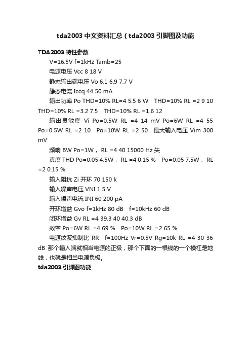
tda2003中文资料汇总(tda2003引脚图及功能TDA2003特性参数V=16.5V f=1kHz T amb=25电源电压 Vcc 8 18 V静态输出端电压 Vo 6.1 6.9 7.7 V静态电流 Iccq 44 50 mA输出功率 Po THD=10% RL=4 5.5 6 W THD=10% RL =2 9 10 THD=10% RL =3.2 7.5 THD=10% RL =1.6 12输出灵敏度Vi Po=0.5W RL =4 14 mV Po=6W RL =4 55 Po=0.5W RL =2 10 Po=10W RL =2 50 最大输入电压 Vim 300 mV频响 BW Po=1W, RL =4 40 15000 Hz 失真度 THD Po=0.05 4.5W, RL =4 0.15 % Po=0.05 7.5W, RL =2 0.15 %输入阻抗 Zi 开环 70 150 k输入噪声电压 VNI 1 5 V输入噪声电流 INI 60 200 pA开环增益 Gvo f=1kHz 80 dB f=10kHz 60 dB闭环增益 Gv RL =4 39.3 40 40.3 dB效率 Po=6W RL =4 69 % Po=10W RL =2 65 %电源纹波抑制比 RR f=100Hz Vr=0.5V Rg=10k RL =4 30 36 dB那个输入端就相当电源的正极,那个下面的一根线的一个横杠是地线,也就是相当电源负极。
tda2003引脚图功能tda2003极限参数tda2003电特性参数tda2003封装外形图tda2003测试电路图直流测试图交流测试图tda2003应用电路一TDA2030采用V型5脚单列直插式塑料封装结构。
如图所示,按引脚的形状引可分为H型和V型。
该集成电路广泛应用于汽车立体声收录音机、中功率音响设备,具有体积小、输出功率大、失真小等特点。
并具有内部保护电路。
维修时常用到的一些小妙招
维修时常用到的一些小妙招4-4-21 13:54:14维修时常用到的一些小妙招闲来无事,坐下来总结几个近来自己维修时用到的小偏方,也欢迎有类似的朋友一起跟帖交流,互相学习。
一,VCD有图无声,把电视打在AV档,接上视频插头,音频插头不插VCD音频输出插座上,外接一104无极电容,手拿电容的令一端,点触解压的音频输出前级端,如果有声,就是运放4558坏了,如手头无备件,应急修法是,断开原机的音频输出端,焊两跟导线直接接在音频输出前级R。
L左右端,即可,此时声音恢复。
二,VCD有声无图,对于视频解压芯片是SPA711的机器,一般是SPA711局部损坏,应急修法是,把电视打在AV档,接上音频插头,视频插头不插VCD音频输出插座上,外接一104无极电容,手拿电容的令一端,点触SPA711的1脚,或其它脚,如果图象出现,则断开原机的视频输出端,用导线连接即可,我用此方法已修复多部机器。
三,对于彩电灯丝碰极的维修方法,可用灯丝旋浮供电,方法是:断开尾板原灯丝供电两端,在行输出变压器上用导线绕2-3圈,用电阻调到和原机灯丝供电电压一样即可修复,用以上几种方法,不用花一分钱即可令机器恢复正常。
对于有些带S端子输出的VCD,可把亮度和色度输出端用101瓷片电容相连,然后接在VCD的视频输出端,也可解决视频解压芯片局部损坏造成的无图象对于开机就暴行管的,应先把串连的逆程电容400V/22N换掉,我发现这种串连的逆程电容不如并连的好,一但此电容失效,开机行管必损无疑.可把串连改为并连,只要总容量一样就行电磁炉电源损坏无配件的应急修理方法:外加15V交流变压器,接在原机18V整流二极管的正极,18V整流二极管的负极串连一IN4007接在原机5V稳压块LA7805的输入端,改装完毕,开机测18V和5V应正常稳定,18V电压不能过高过低,否则易爆IGBTDVD不读碟常见的是,一,排线断,可换一条新的一试. 二,主轴电机坏,用万用表1欧档测主轴电机的正负极,如阻值为几十欧并转速稳定,则电机正常,如阻值很小,电机不转或转速不稳则电机损坏.应急维修可打开电机后罩,清理转子铜头,并把坏的换向铜片换掉既可.电瓶充电机修好后没有电瓶试机法:到汽车配件商店买一个12V/100W的大灯,接在充电机的正负极做负载,此时调流调压是否正常一看便知.否则不接负载电流表不动,用户会说没修好影碟机进出仓不畅的应急维修方法,如没有合适的皮带,或换皮带和电机都不行,可把原皮带轮拿掉,换个直径大一些的皮带轮,如老式录音机上的皮带轮即可,对于进仓后机芯到位不畅,可找一尺寸相当的皮带套在机芯和压碟仓盖上,调整皮带的长度以进出仓灵活金芯并能顺利到为为准,此法已维修多机,屡试屡爽.长虹21寸以及相类似机型,电源起动不良,可直接代换47VF/50V 的电解,最好把电源里的那几个小电解用优质电解全部代换掉.事半功倍.汽车录音机功放块损坏的应急维修方法:用两个TDA2003做一个简单的立体声功放,TDA2003的1脚是输入端接10VF电容接在原机的音频输入端,TDA2003的2脚接一个220VF/25的电容正极,电容的负极接一个220欧的电阻到TDA2003的4脚,电容的负极令一端接一个1欧的电阻接在TDA2003的3脚,TDA2003的3脚是12V的接地端,4脚是放大输出端,通过一个1000VF/16V的电容接在原机的喇叭线上,5脚是12V的正极,做两个一样的电路可组成立体声功放,要求不高的做一个就行了,整个电路只需要两个电阻,两个电容,即可.对于有些功放块难买或价格较贵用此法改装还是比较适合的,此方法我也经常用到.给大家一起分享一下电饭煲无米试锅法:电饭煲修好后,怎么才能知道做饭是否正常?总不会放点米做顿饭试吧.我的方法是:把电饭煲放上适量的水,通电直到烧开后接着烧10分钟,其间没有跳闸外壳也不太热的话,拔下插头,把水倒出,通电,按下煮饭开关,盖上锅盖,大约3分钟左右跳闸的话就说明一切功能正常,如超过5分钟还没有跳闸,并且锅底已冒烟,说明磁缸或开关总成控制杆有问题,换之,如烧水没开就跳闸,则换磁缸或平一下锅胆底部,烧水没开就跳闸,以锅胆底部不平居多.我用此法修电饭煲试锅后,基本没有返修的新买的电烙铁,用用就不好用了,头易烧坏,我的方法是:在电烙铁的手柄处开一方孔大小正好能放下一个微动开关,断开电烙铁的一端连线,在微动开关上焊一个1N4007二极管,开关两端接在电烙铁断开的那两个连线上,把微动开关放入开好的方孔上即可,此时,普通的电烙铁就变成了两档调温电烙铁,平时插电一天也不会烧烙铁头,用时,按住微动开关,即以最高温度工作.许多朋友对于电磁炉暴IGBT管,感到束手无策,冒然换一新的IGBT管,一开机又暴了,苦不堪言。
tda2003
降低带宽
提高带宽
封装外形图
第六页共六页
应用说明图
内部保护电路系统
负载脉冲电压缓冲
在5脚接上LC网络(如应用说明图)可使得TDA2003承受电压脉冲系列,如果电压峰值超过40V,需接入该LC网络,这样可以使5脚上得电压限定在预定值以内(如应用说明图)
如应用说明图接入LC网络后,A处允许有脉冲串(幅度高达120V,脉宽2mS)A处电源电压可大于最高工作电压18V。
39.3
40
40.3
dB
效率
η
f=1kHz
Po=6W, RL=4Ω
Po=10W, RL=2Ω
69
%
65
%
电源电压抑制比
SVR
f=100kHz,Vripple=0.5V
Rg=10kΩ, RL=4Ω
30
36
dB
第三页共六页
TDA2003
应用图
典型应用图
BTL应用图
第四页共六页
TDA2003
简易BTL应用图
短路保护电路(交、直流电)
TDA2003能够持续承受输出端与电源(高至16V)短路
极性反接
器件(TDA2003)能够持续承受大电流(高至5V)而不被损坏直至串接在电源上的1A保险丝被烧断。
对地开路
因4、5脚同有保护二极管TDA2003可接电感性负载,例如耦合变压器。
直流电压
最大直流工作电压18V,然而在28V电压下也不会被损坏,例如在冬天用两节电池串接来启动电机时。
W
RL=8Ω
5.5
6
RL=2Ω
9
10
RL=3.2Ω
7.5
RL=1.6Ω
12
TDA2005R,TDA2005S,TDA2005M, 规格书,Datasheet 资料

5
Package information . . . . . . . . . . . . . . . . . . . . . . . . . . . . . . . . . . . . . . . . 23
6
Revision history . . . . . . . . . . . . . . . . . . . . . . . . . . . . . . . . . . . . . . . . . . . 24
4.1.7 Thermal shut-down . . . . . . . . . . . . . . . . . . . . . . . . . . . . . . . . . . . . . . . . 22
4.1.8 Loudspeaker protection . . . . . . . . . . . . . . . . . . . . . . . . . . . . . . . . . . . . . 22
■ Loudspeaker protection during short circuit for one wire to ground
Description
The TDA2005 is a class B dual audio power amplifier in Multiwatt11 package specifically designed for car radio applications.
4.1.5 Inductive load . . . . . . . . . . . . . . . . . . . . . . . . . . . . . . . . . . . . . . . . . . . . . 21
4.1.6 DC voltage . . . . . . . . . . . . . . . . . . . . . . . . . . . . . . . . . . . . . . . . . . . . . . . 21
TDA2003电路图
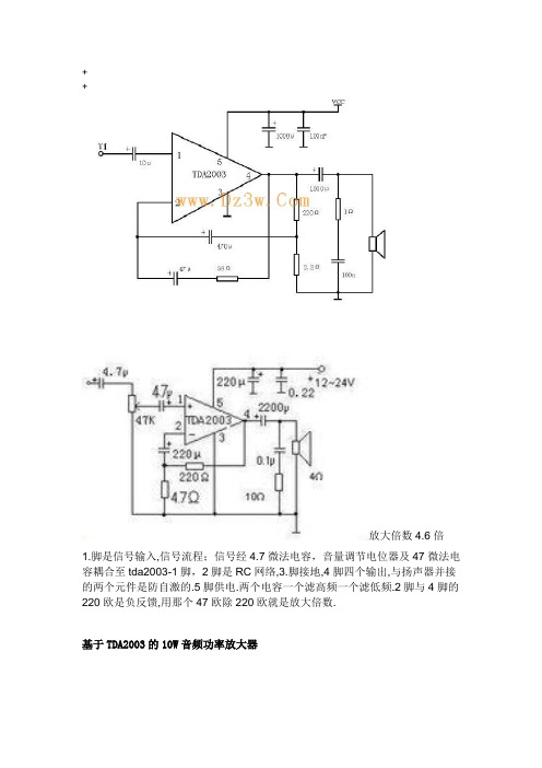
+
+
放大倍数4.6倍
1.脚是信号输入,信号流程;信号经4.7微法电容,音量调节电位器及47微法电容耦合至tda2003-1脚,2脚是RC网络,3.脚接地,4脚四个输出,与扬声器并接的两个元件是防自激的.5脚供电.两个电容一个滤高频一个滤低频.2脚与4脚的220欧是负反馈,用那个47欧除220欧就是放大倍数.
基于TDA2003的10W音频功率放大器
此放大器项目电路可以近似10瓦功率为2欧姆和4欧姆4瓦。
最大功率可以得到16V DC电源和一个2欧姆阻抗扬声器1 A以上的电流。
一个4瓦以上的功率可取得12伏直流电源和1 4欧姆阻抗A以上的电流。
怀旧!上世纪晶体管收音机中常用的这些电子元器件你还记得吗
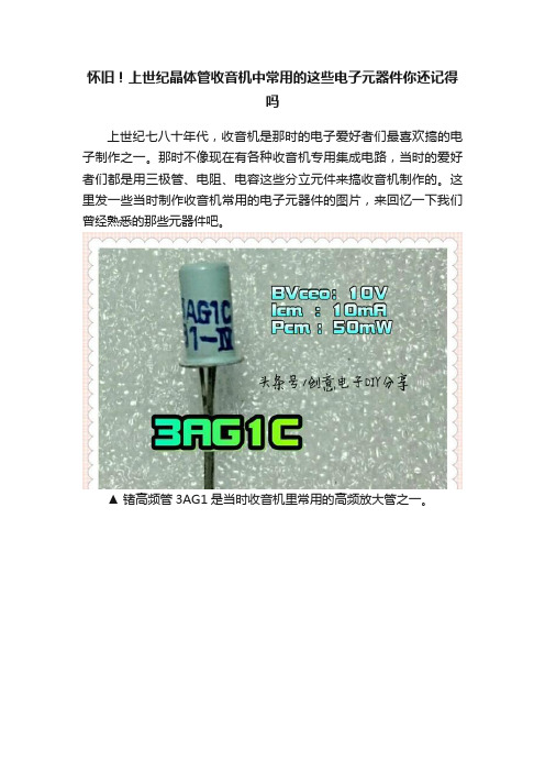
怀旧!上世纪晶体管收音机中常用的这些电子元器件你还记得
吗
上世纪七八十年代,收音机是那时的电子爱好者们最喜欢搞的电子制作之一。
那时不像现在有各种收音机专用集成电路,当时的爱好者们都是用三极管、电阻、电容这些分立元件来搞收音机制作的。
这里发一些当时制作收音机常用的电子元器件的图片,来回忆一下我们曾经熟悉的那些元器件吧。
▲锗高频管3AG1是当时收音机里常用的高频放大管之一。
▲3DG201是当时收音机里常用的NPN型硅三极管,其参数与金属壳封装的3DG6基本一样。
▲ 3DX204与3CX204为互补管,它们常用于OTL功放电路中。
▲2AP9、2AP10锗二极管是当时收音机里最常用的检波二极管。
▲上图所示的铝电解电容为当时收音机里常用的一种电容,其外壳为铝壳,没有绝缘层。
▲这种云母电容也是当时收音机里常用的电容。
▲单管收音机。
这款收音机只用一个锗高频管3AG1放大信号,检波电路用两个2AP9,耳机为高阻抗耳机。
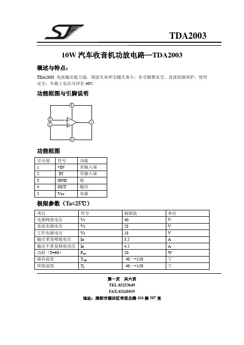
TDA2003芯片介绍

®TDA200310W CAR RADIO AUDIO AMPLIFIERDESCRIPTIONThe TDA 2003has improved performance with the same pin configuration as the TDA 2002.The additional features of TDA 2002,very low numberof externalcomponents,ease of assembly,space and cost saving,are maintained.Thedevice provides a high outputcurrentcapability (up to 3.5A)very low harmonic and cross-over distortion.Completely safe operation is guaranteed due to protectionagainst DC and ACshort circuit between all pins and ground,thermal over-range,load dump voltage surge up to 40V and fortuitous open ground.October 1998Symbol ParameterValue Unit V S Peak supply voltage (50ms)40V V S DC supply voltage 28V V S Operating supply voltage 18V I O Output peak current (repetitive) 3.5A I O Output peak current (non repetitive) 4.5A Ptot Power dissipation at Tcase =90°C 20W T stg ,T jStorage and junction temeperature-40to 150°CABSOLUTE MAXIMUM RATINGSTEST CIRCUITPENTAWATTORDERING NUMBERS :TDA 2003HTDA 2003V1/10TDA2003PIN CONNECTION(top view)SCHEMA TIC DIAGRAMTHERMAL DA TASymbol Parameter Value Unit R th-j-case Thermal resistance junction-case max3°C/W2/10Symbol Parameter Test conditions Min.Typ.Max.Unit DC CHARACTERISTICS(Refer to DC test circuit)V s Supply voltage818V V o Quiescent output voltage(pin4) 6.1 6.97.7VI d Quiescent drain current(pin5)4450mA AC CHARACTERISTICS(Refer to AC test circuit,Gv=40dB)P o Output power d=10%f=1kHz R L=4ΩR L=2ΩR L=3.2ΩR L=1.6Ω5.596107.512WWWWV i(rms)Input saturation voltage300mVV i Input sensitivity f=1kHzP o=0.5WP o=6WP o=0.5WP o10W R L=4ΩR L=4ΩR L=2ΩR L=2Ω14551050mVmVmVmVELECTRICAL CHARACTERISTICS(V s=14.4V,T amb=25°C unless otherwise specified)DC TEST CIRCUIT AC TEST CIRCUIT3/10TDA2003Figure 1.Quiescent output voltage vs.supply voltage Figure 2.Quiescent draincurrent vs.supply voltageFigure3.Output power vs.supply voltageSymbol Parameter Test conditions Min.Typ.Max.UnitB Frequency response(-3dB)P o=1WR L=4Ω40to15,000Hzd Distortion f=1kHzP o=0.05to4.5W R L=4ΩP o=0.05to7.5W R L=2Ω0.150.15%%R i Input resistance(pin1)f=1kHz70150kΩG v Voltage gain(open loop)f=1kHzf=10kHz 8060dBdBG v Voltage gain(closed loop)f=1kHzR L=4Ω39.34040.3dBe N Input noise voltage(0)15µV i N Input noise current(0)60200pAηEfficiency f=1HzP o=6WP o=10W R L=4ΩR L=2Ω6965%%SVR Supply voltage rejection f=100HzV ripple=0.5VR g=10kΩR L=4Ω3036dB ELECTRICAL CHARACTERISTICS(continued)(0)Filter with noise bandwidth:22Hz to22kHzTDA20034/10Figure4.Output power vs. load resistance R L Figure 5.Gain vs.inputsensivityFigure 6.Gain vs.inputsensivityFigure7.Distortion vs. output power Figure8.Distortion vs.frequencyFigure9.Supply voltagerejection vs.voltage gainFigure10.Supply voltage rejection vs.frequency Figure11.Power dissipa-tion and efficiency vs.outputpower(R L=4Ω)Figure12.Power dissipa-tion and efficiencyvs.outputpower(R L=2Ω)5/10TDA2003Figure13.Maximum power dissipation vs.supply voltage (sine wave operation)Figure14.Maximum allowablepower dissipation vs.ambienttemperatureFigure15.Typical values ofcapacitor(C X)for differentvalues of frequency reponse(B)Figure16.Typical application circuit Figure17.P.C.board and component layout for the circuit of fig.16(1:1scale)APPLICATION INFORMA TIONBUIL T-IN PROTECTION SYSTEMS Load dump voltage surgeThe TDA2003has a circuit which enables it to withstand a voltage pulse train,on pin5,of the type shown in fig.19.If the supply voltage peaks to more than40V,then an LC filter must be inserted between the supply and pin5,in order to assure that the pulses at pin 5will be held within the limits shown in fig.18.A suggested LC network is shown in fig.19.With this network,a train of pulses with amplitude up to 120V and width of2ms can be applied at point A. This type of protection is ON when the supply voltage(pulsed or DC)exceeds18V.For thisreason the maximum operating supply voltage is18V.TDA20036/10Short-circuit(AC and DC conditions)The TDA2003can withstand a permanent short-circuit on the output for a supply voltage up to16V. Polarity inversionHigh current(up to5A)can be handled by the device with no damage for a longer period than the blow-out time of a quick1A fuse(normally con-nected in series with the supply).This feature is added to avoid destruction if,during fitting to the car,a mistake on the connectionof the supply is made.Open groundWhen the radio is in the ON condition and the ground is accidentally opened,a standard audio amplifier will be damaged.On the TDA2003pro-tection diodes are included to avoid any damage. Inductive loadA protection diode is provided between pin4and5 (see the internal schematic diagram)to allow use of the TDA2003with inductive loads.In particular,the TDA2003can drive a coupling transformer for audio modulation.DC voltageThe maximum operating DC voltage on the TDA 2003is18V.However the devicecan withstand a DC voltage up to28V with no damage.This could occur during winter if two batteries were series connected to crank the engine.Thermal shut-downThe presence of a thermal limiting circuit offers the following advantages:1)an overload on the output(even if it is perma-nent),oran excessive ambient temperature can be easily withstood.2)the heat-sink can have a smaller factor com-pared with that of a conventionalcircuit.There is no device damage in the case of ex-cessive junction temperature:all that happens is thatP o(andthereforeP tot)andI d are reduced.Figure20.Output power and dra in curre nt vs.c ase temperature(R L=4Ω)Figure21.Output power and drain curre nt vs.c as e temperature(R L=2Ω)Figure18.Figure19.7/10TDA2003Component Recommmendedvalue Purpose Larger thanrecommended valueSmaller thanrecommended value C1C1 2.2µF Input DCdecoupling Noise at switch-on, switch-offC2470µF Ripple rejection Degradation of SVRC30.1µF Supply bypassing Danger of oscillationC41000µF Output coupling to load Higher low frequencycutoffC50.1µF Frequency stability Danger of oscillation athigh frequencies withinductive loadsC X≅12πB R1Upper frequency cutoff Lower bandwidth Larger bandwidthR1(G v-1)•R2Setting of gain Increase of drain currentR2 2.2ΩSetting of gainand SVRDegradation of SVRR31ΩFrequency stability Danger of oscillation athigh frequencies withinductive loadsR X≅20R2Upper frequency cutoff Poor high frequencyattenuation Danger of oscillationPRATICAL CONSIDERA TIONPrinted circuit boardThe layout shown in fig.17is recommended.If different layouts are used,the ground points of input1and input2must be well decoupled from theground of the outputthrough which a ratherhigh current flows.Assembly suggestionNo electrical insulation is required between the packageand the heat-sink.Pin length should be as short as possible.The soldering temperature must not exceed260°C for12seconds.Application suggestionsThe recommended component values are those shown in the application circuits of fig.16. Different values can be used.The following table is intended to aid the car-radio designer.8/10TDA2003Pentawatt VDIM.mm inch MIN.TYP.MAX.MIN.TYP.MAX.A 4.80.189C 1.370.054 D 2.4 2.80.0940.110D1 1.2 1.350.0470.053E 0.350.550.0140.022E10.76 1.190.0300.047F 0.8 1.050.0310.041F11 1.40.0390.055G 3.2 3.4 3.60.1260.1340.142G1 6.6 6.870.2600.2680.276H210.40.409H310.0510.40.3960.409L 17.5517.8518.150.6910.7030.715L115.5515.7515.950.6120.6200.628L221.221.421.60.8310.8430.850L322.322.522.70.8780.8860.894L4 1.290.051L5 2.630.1020.118L615.115.80.5940.622 L76 6.60.2360.260L90.20.008M 4.23 4.5 4.750.1670.1770.187M1 3.7544.250.1480.1570.167V440°(typ.)L L1ACL5D1L2L3EM1MDH3Dia.L7L6F1H2F G G1E1F EL9V4RR RRESIN BETWEENLEADSH1V3H2L8VV V1BV VV4V4OUTLINE AND MECHANICAL DATA9/10TDA2003TDA2003Information furnished is believed to be accurate and reliable.However,STMicroelectronics assumes no responsibility for the consequences of use of such information nor for any infringement of patents or other rights of third parties which may result from its use.No license is granted by implication or otherwise under any patent or patent rights of STMicroelectronics.Specification mentioned in this publication are subject to change without notice.This publication supersedes and replaces all information previously supplied.STMicroelectronics products are not authorized for use as critical components in life support devices or systems without express written approval of STMicroelectronics.The ST logo is a registered trademark of STMicroelectronics©1998STMicroelectronic s–Printed in Italy–All Rights ReservedSTMicroelectronics GROUP OF COMPANIESAustralia-Brazil-Canada-China-France-Germany-Italy-Japan-Korea-Malaysia-Malta-Mexico-Morocco-The Netherlands-Singapore-Spain-Sweden-Switzerland-Taiwan-Thailand-United Kingdom-U.S.A.10/10Copyright © Each Manufacturing Company.All Datasheets cannot be modified without permission.This datasheet has been download from :100% Free DataSheet Search Site.Free Download.No Register.Fast Search System.。
tda2003参数资料

tda2003参数资料2008年03月09日11:23 本站原创作者:本站用户评论(0)关键字:tda2003的特点:TDA2003电流输出能力强,谐波失真和交越失真小,各引脚都有交,直流短路保护,使用安全,负载上电压可冲至40V.TDA2003的引脚功能和管脚定义最大额定值Tamb=25参数名称符号极限值单位电源峰值电压(50mS) Vccp 40 V直流电源电压Vcc 28 V工作电源电压Vcc 18 V输出重复峰值电压Io 3.5 A输出不重复峰值电压Io 4.5 A功耗T=90 PD 20 W储存温度Tstg -40 +150度焊接温度Tj -40 +150 度电特性参数除非特别说明V=16.5V f=1kHz Tamb=25参数名称符号测试条件最小值典型值最大值单位电源电压Vcc 8 18 V静态输出端电压Vo 6.1 6.9 7.7 V静态电流Iccq 44 50 mA 输出功率Po THD=10% RL=4 5.5 6 WTHD=10% RL =2 9 10THD=10% RL =3.2 7.5THD=10% RL =1.6 12输出灵敏度Vi Po=0.5W RL =4 14 mV Po=6W RL =4 55Po=0.5W RL =2 10Po=10W RL =2 50最大输入电压Vim 300 mV 频响BW Po=1W, RL =4 40 15000 Hz 失真度THD Po=0.05 4.5W, RL =4 0.15 %Po=0.05 7.5W, RL =2 0.15 %输入阻抗Zi 开环70 150 k输入噪声电压VNI 1 5 V输入噪声电流INI 60 200 pA开环增益Gvo f=1kHz 80 dBf=10kHz 60 dB闭环增益Gv RL =4 39.3 40 40.3 dB效率Po=6W RL =4 69 %Po=10W RL =2 65 %电源纹波抑制比RRf=100Hz Vr=0.5V Rg=10k RL =4 30 36 dB。
- 1、下载文档前请自行甄别文档内容的完整性,平台不提供额外的编辑、内容补充、找答案等附加服务。
- 2、"仅部分预览"的文档,不可在线预览部分如存在完整性等问题,可反馈申请退款(可完整预览的文档不适用该条件!)。
- 3、如文档侵犯您的权益,请联系客服反馈,我们会尽快为您处理(人工客服工作时间:9:00-18:30)。
®TDA200310W CAR RADIO AUDIO AMPLIFIERDESCRIPTIONThe TDA 2003has improved performance with the same pin configuration as the TDA 2002.The additional features of TDA 2002,very low numberof externalcomponents,ease of assembly,space and cost saving,are maintained.Thedevice provides a high outputcurrentcapability (up to 3.5A)very low harmonic and cross-over distortion.Completely safe operation is guaranteed due to protectionagainst DC and ACshort circuit between all pins and ground,thermal over-range,load dump voltage surge up to 40V and fortuitous open ground.October 1998Symbol ParameterValue Unit V S Peak supply voltage (50ms)40V V S DC supply voltage 28V V S Operating supply voltage 18V I O Output peak current (repetitive) 3.5A I O Output peak current (non repetitive) 4.5A Ptot Power dissipation at Tcase =90°C 20W T stg ,T jStorage and junction temeperature-40to 150°CABSOLUTE MAXIMUM RATINGSTEST CIRCUITPENTAWATTORDERING NUMBERS :TDA 2003HTDA 2003V1/10TDA2003PIN CONNECTION(top view)SCHEMA TIC DIAGRAMTHERMAL DA TASymbol Parameter Value Unit R th-j-case Thermal resistance junction-case max3°C/W2/10Symbol Parameter Test conditions Min.Typ.Max.Unit DC CHARACTERISTICS(Refer to DC test circuit)V s Supply voltage818V V o Quiescent output voltage(pin4) 6.1 6.97.7VI d Quiescent drain current(pin5)4450mA AC CHARACTERISTICS(Refer to AC test circuit,Gv=40dB)P o Output power d=10%f=1kHz R L=4ΩR L=2ΩR L=3.2ΩR L=1.6Ω5.596107.512WWWWV i(rms)Input saturation voltage300mVV i Input sensitivity f=1kHzP o=0.5WP o=6WP o=0.5WP o10W R L=4ΩR L=4ΩR L=2ΩR L=2Ω14551050mVmVmVmVELECTRICAL CHARACTERISTICS(V s=14.4V,T amb=25°C unless otherwise specified)DC TEST CIRCUIT AC TEST CIRCUIT3/10TDA2003Figure 1.Quiescent output voltage vs.supply voltage Figure 2.Quiescent draincurrent vs.supply voltageFigure3.Output power vs.supply voltageSymbol Parameter Test conditions Min.Typ.Max.UnitB Frequency response(-3dB)P o=1WR L=4Ω40to15,000Hzd Distortion f=1kHzP o=0.05to4.5W R L=4ΩP o=0.05to7.5W R L=2Ω0.150.15%%R i Input resistance(pin1)f=1kHz70150kΩG v Voltage gain(open loop)f=1kHzf=10kHz 8060dBdBG v Voltage gain(closed loop)f=1kHzR L=4Ω39.34040.3dBe N Input noise voltage(0)15µV i N Input noise current(0)60200pAηEfficiency f=1HzP o=6WP o=10W R L=4ΩR L=2Ω6965%%SVR Supply voltage rejection f=100HzV ripple=0.5VR g=10kΩR L=4Ω3036dB ELECTRICAL CHARACTERISTICS(continued)(0)Filter with noise bandwidth:22Hz to22kHzTDA20034/10Figure4.Output power vs. load resistance R L Figure 5.Gain vs.inputsensivityFigure 6.Gain vs.inputsensivityFigure7.Distortion vs. output power Figure8.Distortion vs.frequencyFigure9.Supply voltagerejection vs.voltage gainFigure10.Supply voltage rejection vs.frequency Figure11.Power dissipa-tion and efficiency vs.outputpower(R L=4Ω)Figure12.Power dissipa-tion and efficiencyvs.outputpower(R L=2Ω)5/10TDA2003Figure13.Maximum power dissipation vs.supply voltage (sine wave operation)Figure14.Maximum allowablepower dissipation vs.ambienttemperatureFigure15.Typical values ofcapacitor(C X)for differentvalues of frequency reponse(B)Figure16.Typical application circuit Figure17.P.C.board and component layout for the circuit of fig.16(1:1scale)APPLICATION INFORMA TIONBUIL T-IN PROTECTION SYSTEMS Load dump voltage surgeThe TDA2003has a circuit which enables it to withstand a voltage pulse train,on pin5,of the type shown in fig.19.If the supply voltage peaks to more than40V,then an LC filter must be inserted between the supply and pin5,in order to assure that the pulses at pin 5will be held within the limits shown in fig.18.A suggested LC network is shown in fig.19.With this network,a train of pulses with amplitude up to 120V and width of2ms can be applied at point A. This type of protection is ON when the supply voltage(pulsed or DC)exceeds18V.For thisreason the maximum operating supply voltage is18V.TDA20036/10Short-circuit(AC and DC conditions)The TDA2003can withstand a permanent short-circuit on the output for a supply voltage up to16V. Polarity inversionHigh current(up to5A)can be handled by the device with no damage for a longer period than the blow-out time of a quick1A fuse(normally con-nected in series with the supply).This feature is added to avoid destruction if,during fitting to the car,a mistake on the connectionof the supply is made.Open groundWhen the radio is in the ON condition and the ground is accidentally opened,a standard audio amplifier will be damaged.On the TDA2003pro-tection diodes are included to avoid any damage. Inductive loadA protection diode is provided between pin4and5 (see the internal schematic diagram)to allow use of the TDA2003with inductive loads.In particular,the TDA2003can drive a coupling transformer for audio modulation.DC voltageThe maximum operating DC voltage on the TDA 2003is18V.However the devicecan withstand a DC voltage up to28V with no damage.This could occur during winter if two batteries were series connected to crank the engine.Thermal shut-downThe presence of a thermal limiting circuit offers the following advantages:1)an overload on the output(even if it is perma-nent),oran excessive ambient temperature can be easily withstood.2)the heat-sink can have a smaller factor com-pared with that of a conventionalcircuit.There is no device damage in the case of ex-cessive junction temperature:all that happens is thatP o(andthereforeP tot)andI d are reduced.Figure20.Output power and dra in curre nt vs.c ase temperature(R L=4Ω)Figure21.Output power and drain curre nt vs.c as e temperature(R L=2Ω)Figure18.Figure19.7/10TDA2003Component Recommmendedvalue Purpose Larger thanrecommended valueSmaller thanrecommended value C1C1 2.2µF Input DCdecoupling Noise at switch-on, switch-offC2470µF Ripple rejection Degradation of SVRC30.1µF Supply bypassing Danger of oscillationC41000µF Output coupling to load Higher low frequencycutoffC50.1µF Frequency stability Danger of oscillation athigh frequencies withinductive loadsC X≅12πB R1Upper frequency cutoff Lower bandwidth Larger bandwidthR1(G v-1)•R2Setting of gain Increase of drain currentR2 2.2ΩSetting of gainand SVRDegradation of SVRR31ΩFrequency stability Danger of oscillation athigh frequencies withinductive loadsR X≅20R2Upper frequency cutoff Poor high frequencyattenuation Danger of oscillationPRATICAL CONSIDERA TIONPrinted circuit boardThe layout shown in fig.17is recommended.If different layouts are used,the ground points of input1and input2must be well decoupled from theground of the outputthrough which a ratherhigh current flows.Assembly suggestionNo electrical insulation is required between the packageand the heat-sink.Pin length should be as short as possible.The soldering temperature must not exceed260°C for12seconds.Application suggestionsThe recommended component values are those shown in the application circuits of fig.16. Different values can be used.The following table is intended to aid the car-radio designer.8/10TDA2003Pentawatt VDIM.mm inch MIN.TYP.MAX.MIN.TYP.MAX.A 4.80.189C 1.370.054 D 2.4 2.80.0940.110D1 1.2 1.350.0470.053E 0.350.550.0140.022E10.76 1.190.0300.047F 0.8 1.050.0310.041F11 1.40.0390.055G 3.2 3.4 3.60.1260.1340.142G1 6.6 6.870.2600.2680.276H210.40.409H310.0510.40.3960.409L 17.5517.8518.150.6910.7030.715L115.5515.7515.950.6120.6200.628L221.221.421.60.8310.8430.850L322.322.522.70.8780.8860.894L4 1.290.051L5 2.630.1020.118L615.115.80.5940.622 L76 6.60.2360.260L90.20.008M 4.23 4.5 4.750.1670.1770.187M1 3.7544.250.1480.1570.167V440°(typ.)L L1ACL5D1L2L3EM1MDH3Dia.L7L6F1H2F G G1E1F EL9V4RR RRESIN BETWEENLEADSH1V3H2L8VV V1BV VV4V4OUTLINE AND MECHANICAL DATA9/10TDA2003TDA2003Information furnished is believed to be accurate and reliable.However,STMicroelectronics assumes no responsibility for the consequences of use of such information nor for any infringement of patents or other rights of third parties which may result from its use.No license is granted by implication or otherwise under any patent or patent rights of STMicroelectronics.Specification mentioned in this publication are subject to change without notice.This publication supersedes and replaces all information previously supplied.STMicroelectronics products are not authorized for use as critical components in life support devices or systems without express written approval of STMicroelectronics.The ST logo is a registered trademark of STMicroelectronics©1998STMicroelectronic s–Printed in Italy–All Rights ReservedSTMicroelectronics GROUP OF COMPANIESAustralia-Brazil-Canada-China-France-Germany-Italy-Japan-Korea-Malaysia-Malta-Mexico-Morocco-The Netherlands-Singapore-Spain-Sweden-Switzerland-Taiwan-Thailand-United Kingdom-U.S.A.10/10。