EBE25RC8AAFA-4C-E中文资料
德国睿克斯电机样本
Encoder setting 4
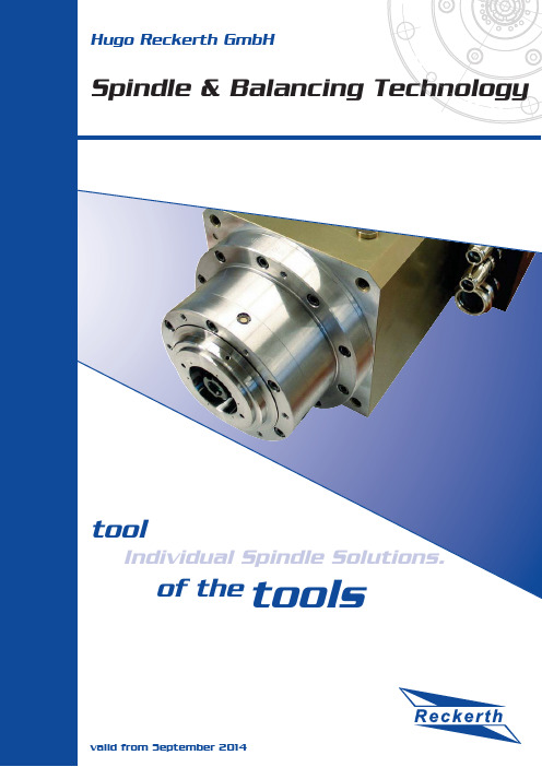
1. Motor spindles with HSK interface
Our line of motor spindles has experienced very diverse development over the last several years. 7KHSURGXFWUDQJHFRQVLVWVRIPRGHOVIRUJULQGLQJGULOOLQJDQGPLOOLQJDSSOLFDWLRQVZKRVHVWUHQJWKLVHVSHFLDOO\ based on high-speed processing. A large selection of product options and additional options is available. Spindle attributes: • • • • • • • • Compact design Asynchronous or synchronous motor Cylindrical or prismatic housing Manual or automatic tool changer Water or air cooling Sealing air to protect the inside of the spindle against contamination +LJKWUXHUXQQLQJDFFXUDF\LQWKHWDSHUPP Ball bearing with continuous grease lubrication or oil-air lubrication system Rigidity variation options (adapted to the customer's speed requirement):
施奈德EOCR保护器新产品中文版
Emission
& 7
i3DM / iFDM, i3MZ/iFMZ, i3MS/iFMS, i3M420/iFM420, i3BZ/iFBZ
0.5~60A, 60A ,
i3MS/iFMS 0.5~20A, 20A ,
& TCC 0.5~32A, 32A
i3BZ iFBZ
2
0.5A
D-time O-time
3BZ2 / FBZ2 AC/DC 100~240V
DC/AC 24V 50/60 Hz
i3DM / iFD AC/DC 100~2
DC/AC 24 50/60 Hz
A, F, H
5 Digit 7 Segment -
/ 3DD, 3DE, 3DM FD, FDE, FDM
-
5 Digit 7 Segment -
DC/AC 24V 50/60 Hz
i3MZ / iFMZ AC/DC 100~240V
DC/AC 24V 50/60 Hz
i3BZ / iFBZ AC/DC 100~240V
DC/AC 24V 50/60 Hz
i3M420 / iFM420 AC/DC 100~240V
DC/AC 24V 50/60 Hz
EOCR-iFDM (Z, S, 420) Window type
EOCR-iFDM (Z, S, 420, BZ) Bottom hole type
EOCR-i3DM (Z, S, 420, BZ) Terminal type
EOCR-iFDM (Z, S, 420, BZ) Terminal type
IEC61000-4-2 IEC61000-4-3 IEC61000-4-6 IEC61000-4-4 IEC61000-4-5 CISPR11
M80C85资料
GENRAL DESCRIPTIONThe MSM80C85AH is a complete 8-bit parallel; central processor implemented in silicon gate C-MOS technology and compatible with MSM80C85A.It is designed with higher processing speed (max.5 MHz) and lower power consumption compared with MSM80C85A and power down mode is provided, thereby offering a high level of system integration.The MSM80C85AH uses a multiplexed address/data bus. The address is split between the 8-bit address bus and the 8-bit data bus. The on-chip address latch : of a MSM81C55-5 memory product allows a direct interface with the MSM80C85AH.FEATURES•Power down mode (HALT-HOLD)•Low Power Dissipation: 50mW(Typ)•Single + 3 to + 6 V Power Supply•–40 to + 85°C, Operating Temperature •Compatible with MSM80C85A •0.8 m s instruction Cycle (V CC = 5V)•On-Chip Clock Generator (with External Crystal)•On-Chip System Controller; Advanced Cycle Status Information Available for Large System Control•Bug operation in MSM80C85AH is fixed•Four Vectored interrupt (One is non-maskable) Plus the 8080A-compatible interrupt.•Serial, In/Serial Out Port•Decimal, Binary and Double Precision Arithmetic •Addressing Capability to 64K Bytes of Memory •TTL Compatible•40-pin Plastic DIP(DIP40-P-600-2.54): (Product name: MSM80C85AHRS)•44-pin Plastic QFJ(QFJ44-P-S650-1.27): (Product name: MSM80C85AHJS)•44-pin Plastic QFP(QFP44-P-910-0.80-2K): (Product name: MSM80C85AHGS-2K)MSM80C85AHRS/GS/JS8-Bit CMOS MICROPROCESSORE2O0009-27-X2元器件交易网FUNCTIONAL BLOCK DIAGRAMINTR INTA 5.5 6.57.5TRAP SID SODRSTX1X2CLK OUT READY RD WR ALE S0S1IO / M HOLD HLDA RESET IN RESET OUT A15 - A8Address BusAD7- ADAddress/Data BusPIN CONFIGURATION (TOP VIEW)40 pin Plastic DIPA 8HOLD HLDA CLK(OUT)RESET IN READY IO/M S 1RD WR ALE S 0A 15A 14A 13A 12A 11A 10A 9V CC 39383736353433READY IO/M S 1RD WR NC ALE TRAP RST7.5RST6.5RST5.5INTR NC INTA 18192021222324A D 4N C A D 5A D 6A D 7G N D A 865432144S I DS O DR E S E T X 2X 1N C7891011121332313029S 0A 15A 14AD 0AD 1AD 2AD 314151617A 13V C C25262728A 9A 10A 11A 1243424140H O L D H L D AC L K (O R E S E T I NTRAP RST7.5RST6.5RST5.5INTR INTA AD 0A D 4A D 5A D 6A D 7G N D V C C A 8AD 1AD 2AD 3NC A 9A 10A 11N CMSM80C85AH FUNCTIONAL PIN DEFINITIONThe following describes the function of each pin:A 0 - A 7(Input/Output)3-state A 8 - A 15(Output, 3-state)Multiplexed Address/Data Bus: Lower 8-bits of the memory address (or I/O address) appear on the bus during the first clock cycle (T state) of a machine cycle. It then becomes the data bus during the second and third clock cycles.Address Bus: The most significant 8-bits of the memory address or the 8-bits of the I/O address, 3-stated during Hold and Halt modes and during RESET.Symbol FunctionALE (Output)Address Latch Enable: It occurs during the first clock state of a machine cycle and enables address to get latched into the on-chip latch peripherals. The falling edge of ALE is set to guarantee setup and hold times for the address information. The falling edge ALE can also be used to strobe the status information ALE is never 3-state.S 0 , S 1 , IO/M (Output)Machine cycle status:IO/M S 1 S 0 States S 1 can be used as an advanced R/W status. IO/M , S 0 and S 1 become valid at the beginning ofa machine cycle and remain stable throughout the cycle. The falling edge of ALE may be used to latch the state of these lines.RD(Output, 3-state)READ control: A low level on RD indicates the selected memory or I/O device is to be read thatthe Data Bus is available for the data transfer, 3-stated during Hold and Halt modes and during RESET.WR(Output, 3-state)WRITE control: A low level on WR indicates the data on the Data Bus is to be written into the selected memory or I/O location. Data is set up at the trailing edge of WR , 3-stated during Hold and Halt modes and during RESET.READY (Input)If READY is high during a read or write cycle, it indicates that the memory or peripheral is ready to send or receive data. If READY is low, the cpu will wait an integral number of clock cycles for READY to go high before completing the read or write cycle READY must conform to specified setup and hold times.HOLD (Input)HLDA (Output)HOLD ACKNOWLEDGE: Indicates that the cpu has received the HOLD request and that it will relinquish the bus in the next clock cycle. HLDA goes low after the Hold request is removed. The cpu takes the bus one half clock cycle after HLDA goes low.HOLD indicates that another master is requesting the use of the address and data buses.The cpu, upon receiving the hold request, will relinquish the use of the bus as soon as the completion of the current bus transfer. Internal processing can continue. The processor can regain the bus only after the HOLD is removed. When the HOLD is acknowledged, the Address, Data, RD , WR , and IO/M lines are 3-stated. And status of power down is controlled by HOLD.INTR (Output)INTERRUPT REQUEST: Is used as a general purpose interrupt. It is sampled on during the next to the last clock cycle of an instruction and during Hold and Halt states. If it is active, the Program Counter (PC) will be inhibited from incrementing and an INTA will be issued. During this cycle a RESTART or CALL instruction can be inserted to jump to the interrupt service routine. The INTR is enabled and disabled by software. It is disabled by Reset and immediately after an interrupt is accepted. Power down mode is reset by INTR.INTA (Output)INTERRUPT ACKNOWLEDGE: Is used instead of (and has the same timing as) RD during the instruction cycle after an INTR is accepted.RST 5.5RST 6.5RST 7.5(Input)RESTART INTERRUPTS: These three inputs have the same timing as INTR except they cause an internal RESTART to be automatically inserted.The priority of these interrupts is ordered as shown in Table 1. These interrupts have a higher priority than INTR. In addition, they may be individually masked out using the SIM instruction. Power down mode is reset by these interrupts.TRAP (Input)Trap interrupt is a nonmaskable RESTART interrupt. It is recognized at the same timing as INTR or RST 5.5 - 7.5. It is unaffected by any mask or Interrupt Disable. It has the highest priority of any interrupt. (See Table 1.) Power down mode is reset by input of TRAP.001100101110101Memory write Memory read I/O write I/O readOpcode fetchIO/M S 1 S 0 States 1...10¥¥10¥¥Interrupt Acknowledge Halt = 3-stateHold (high impedance)Reset ¥ = unspecifiedName Address Branched To (1)When Interrupt OccursType TriggerRST 7.53CH 34H Rising edge (latched).High level unitl sampled.RST 6.5RST 5.52CH (2)High level until sampled.High level until sampled.INTRTRAP Priority 2345124H Rising edge and high level unit sampled.Table 1 Interrupt Priority, Restart Address, and SensitivityNotes:(1)The processor pushes the PC on the stack before branching to the indicatedaddress.(2)The address branched to depends on the instruction provided to the cpuwhen the interrupt is acknowledged.RESET IN (Input)Sets the Program Counter to zero and resets the Interrupt Enable and HLDA flip-flops and release power down mode. The data and address buses and the control lines are 3-stated during RESET and because of the asynchronous nature of RESET IN, the processor's internal registers and flags may be altered by RESET with unpredictable results. RESET IN is a Schmitt-triggered input, allowing connection to an R-C network for power-on RESET delay. The cpu is held in the reset condition as long as RESET IN is applied.Symbol FunctionRESET OUT (Output)Indicated cpu is being reset. Can be used as a system reset. The signal is synchronized to the processor clock and lasts an integral number of clock periods.X 1, X 2(Input)X 1 and X 2 are connected to a crystal to drive the internal clock generator. X 1 can also be an external clock input from a logic gate. The input frequency is divided by 2 to give the processor's internal operating frequency.SID (Input)Serial input data line. The data on this line is loaded into accumulator bit 7 whenever a RIM instruction is executed.SOD (Output)Serial output data line. The output SOD is set or reset as specified by the SIM instruction.V CC + 5 Volt supply GNDGround Reference.CLK (Output)Clock Output for use as a system clock. The period of CLK is twice the X 1, X 2 input period.FUNCTIONAL DESCRIPTIONThe MSM80C85AH is a complete 8-bit parallel central processor. It is designed with silicon gate C-MOS technology and requires a single +5 volt supply. Its basic clock speed is 5 MHz, thus improving on the present MSM80C85A's performance with higher system speed and power down mode. Also it is designed to fit into a minimum system of two IC's: The CPU (MSM80C85AH), and a RAM/IO (MSM81C55-5)The MSM80C85AH has twelve addressable 8-bit register pairs. Six others can be used interchangeably as 8-bit registers or 16-bit register pairs. The MSM80C85AH register set is as follows:PC 16-bit address 8-bit ¥ 6 or 16-bits ¥ 3BC, DE, HL SP 16-bit address 5 flags (8-bit space)Flags or FProgram CounterACC or A 8-bits Accumulator Mnemonic ContentsRegisterGeneral-Purpose Registers; data pointer (HL)Stack Pointer Flag RegisterThe MSM80C85AH uses a multiplexed Data Bus. The address is spilt between the higher 8-bit Address Bus and the lower 8-bit Address/Data Bus. During the first T state (clock cycle) of a machine cycle the low order address is sent out on the Address/Data Bus. These lower 8-bits may be latched externally by the Address Latch Enable signal (ALE). During the rest of the machine cycle the data bus is used for mamory or I/O data.The MSM80C85AH provides RD , WR , S 0, S 1, and IO/M signals for bus control. An Interrupt Acknowledge signal (INTA ) is also provided. Hold and all Interrupts are synchronized with the processor's internal clock. The MSM80C85AH also provides Serial Input Data (SID) and Serial Output Data (SOD) lines for a simple serial interface.In addition to these features, the MSM80C85AH has three maskable, vector interrupt pins, one nonmaskable TRAP interrupt and power down mode with HALT and HOLD.INTERRUPT AND SERIAL I/OThe MSM80C85AH has 5 interrupt inputs: INTR, RST 5.5 RST 6.5, RST 7.5, and TRAP. INTR is identical in function to the 8080A INT. Each of the three RESTART inputs, 5.5, 6.5, and 7.5, has a programmable mask. TRAP is also a RESTART interrupt but it is nonmaskable.The three maskable interrupts cause the internal execution of RESTART ( saving the program counter in the stack branching to the RESTART address) it the interrupts are enable and if the interrupt mask is not set. The nonmaskable TRAP causes the internal execution of a RESTART vector independent of the state of the interrupt enable or masks. (See Table 1.)There are two different types of inputs in the restart interrupt. RST 5.5 and RST 6.5 are high level-sensitive like INTR (and INT on the 8080A) and are recognized with the same timing as INTR. RST 7.5 is rising edge-sensitive.For RST 7.5, only a pulse is required to set an internal flip-flop which generates the internal interrupt request. The RST 7.5 request flip-flop remains set until the request is serviced. Then it is reset automatically, This flip-flop may also be reset by using the SIM instruction or by issuing a RESET␣IN to the MSM80C85AH. The RST 7.5 internal flip-flop will be set by a pulse on the RST 7.5 pin even when the RST 7.5 interrupt is masked out.The interrupts are arranged in a flixed priority that determines which interrupt is to be recognized if more than one is pending, as follows: TRAP-highest priority, RST 7.5, RST 6.5, RST 5.5, INTR-lowest priority. This priority scheme does not take into account the priority of a routine that was started by a higher priority interrupt. RST 5.5 can interrupt an RST 7.5 routine if the interrupt are re-enabled before the end of the RST 7.5 routine.The TRAP interrupt is useful for catastrophic evens such as power failure or bus error. The TRAP input is recognized just as any other interrupt but has the highest priority. It is not affected by any flag or mask. The TRAP input is both edge and level sensitive. The TRAP input must go high and remain high until it is acknowledged. It will not be recognized again until it goes low, then high again. This avoids any false triggering due to noise or logic glitches. Figure 3 illustrates the TRAP interrupt request circuitry within the MSM80C85AH. Note that the servicing of any interrupt (TRAP, RST 7.5, RST 6.5, RST 5.5,INTR) disables all future interrupts (except TRAPs) until an El instruction is executed.The TRAP interrupt is special in that it disables interrupts, but preserves the previous interrupt enable status. Performing the first RIM instruction following a TRAP interrupt allows you to determine whether interrupts were enabled or disabled prior to the TRAP. All subsequent RIM instructions provide current interrupt enable status. Performing a RIM instruction following INTR or RST 5.5-7.5 will provide current interrupt Enable status, revealing that Interrupts are disabled.The serial I/O system is also controlled by the RIM and SIM instructions. SID is read by RIM, and SIM sets the SOD data.AcknowledgeFigure 3 Trap and RESET IN CircuitDRIVING THE X 1 AND X 2 INPUTSYou may drive the clock inputs of the MSM80C85AH with a crystal, or an external clock source.The driving frequency must be at least 1 MHz, and must be twice the desired internal clock frequency; hence, the MSM80C85AH is operated with a 6 MHz crystal (for 3 MHz clock). If a crystal is used, it must have the following characteristics:Parallel resonance at twice the clock frequency desired C L (load capacitance) £ 30 pF C S (shunt capacitance) £ 7 pFR S (equivalent shunt resistance) £ 75 ohms Drive level: 10 mWFrequency tolerance: ±0.05% (suggested)Note the use of the capacitors between X 1, X 2 and ground. These capacitors are required to assure oscillator startup at the correct frequency.Figure 4 shows the recommended clock driver circuits. Note in B that a pull-up resistor is required to assure that the high level voltage of the input is at least 4 V.For driving frequencies up to and including 6 MHz you may supply the driving signal to X, and leave X 2 open-circuited (Figure 4B). To prevent self-oscillation of the MSM80C85AH, be sure that X 2 is not coupled back to X 1 through the driving circuit.Note:Since the constant values may vary depending on oscillator, consult the manufacturer of the oscillator used when designing a circuit.Figure 4 Clock Driver Circuits* X 2 Left Floating33 pF Capacitor required for crystal frequency 10 to 6.25 MHz 50 pF Capacitor required for crystal frequency 6.25 to 4 MHz 100 pF Capacitor required for crystal frequency <4 MHzA. Quartz Crystal Clock DriverB. 1 - 10 MHz Input Frequency External Clock Drive CircuitBASIC SYSTEM TIMINGThe MSM80C85AH has a multiplexed Data Bus. ALE is used as a strobe to sample the lower 8-bits of address on the Data Bus. Figure 5 shows an instruction fetch, memory read and I/O write cycle (as would occur during processing of the OUT instruction). Note that during the I/ O write and read cycle that the I/O port address is copied on both the upper and lower half of the address.There are seven possible types of machine cycles. Which of these seven takes place is defined by the status of the three status lines (IO/M, S1, S0) and the three control signals (RD, WR,and INTA). (See Table 2.) The status line can be used as advanced controls (for device selection, for example), since they become active at the T1 state, at the outset of each machine cycle. Control lines RD and WR become active later, at the time when the transfer of data is to take place, so are used as command lines.A machine cycle normally consists of three T states, with the exception of OPCODE FETCH, which normally has either four or six T states (unless WAIT or HOLD states are forced by the receipt of READY or HOLD inputs). Any T state must be one of ten possible states, shown in Table 3.Table 2 MSM80C85AH Machine Cycle ChartTable 3 MSM80C85AH Machine State Chart0= Logic "0"1= Logic "1"TS = High Impedance ¥= UnspecifiedNotes:(1) ALE not generated during 2nd and 3rd machine cycles of DAD instruction.(2) IO/M = 1 during T 4 - T 6 of INA machine cycle.A AD IO/Figure 5 MSM80C85AH Basic System TimingPOWER DOWN ModeThe MSM80C85AH is compatible with the MSM80C85A in function and POWER DOWN mode. This reduces power consumption further.There are two methods available for starting this POWER DOWN mode. One is through software control by using the HALT command and the other is under hardware control by using the pin HOLD. This mode is released by the HOLD, RESET, and interrupt pins (TRAP, RST7.5, RST6.5 RST5.5, or INTR). (See Table 4.)Since the sequence of HALT, HOLD, RESET, and INTERRUPT is compatible with MSM80C85A, every the POWER DOWN mode can be used with no special attention.Start by means of Halt command Start by means of HOLD pin Released by using pins RESET and INTERRUPT (not by pin HOLD) Released by using RESET and HOLD pins (not by interrupt pins)Table 4 POWER DOWN Mode Releasing Method(1) Start by means of HALT command (See Figures 6 and 7.)The POWER DOWN mode can be started by executing the HALT command.At this time, the system is put into the HOLD status and therefore the POWER DOWN mode cannot be released even when the HOLD is released later.In this case, the POWER DOWN mode can be released by means of the RESET or interrupt.(2) Start by means of HOLD pin (See Figure 8.)During the execution of commands other than the HALT, the POWER DOWN mode is started when the system is put into HOLD status by means of the HOLD pin.Since no interrupt works during the execution of the HOLD, the POWER DOWN mode cannot be released by means of interrupt pins. In this case, the POWER DOWN mode can be released either by means of the RESET pin or by releasing the HOLD status by means of HOLD pin.CLK (OUT)ALEAD 0-7CPU MODE RESET INFigure 6 Started by HALT and Released by RESET INCLK (OUT)ALEHOLD CPU MODEHLDAFigure 8 Started and Released by HOLDCLK (OUT)ALECPU MODERST5.5Figure 7 Started by HALT and Released by RST5.5ABSOLUTE MAXIMUM RATINGS–55 - +150MSM80C85AHRS Power Supply Voltage V CC –0.5 - 7V Input Voltage V IN –0.5 - V CC +0.5V Output Voltage V OUT –0.5 - V CC +0.5V Storage Temperature T STG °CPower DissipationP D0.7WParameter Units Symbol With respect to GND—Ta = 25°CCondition LimitsMSM80C85AHGS MSM80C85AHJS1.01.0OPERATING RANGELimits Power Supply Voltage V CC 3 - 6V Operating TemperatureT OP–40 - +85°CParameterUnit Symbol RECOMMENDED OPERATING CONDITIONSDC CHARACTERISTICS"L"V ILR —–0.3+0.8Typ.Power Supply Voltage V CC 5V T OP +25"L" Input Voltage V IL —"H" Output Voltage V IH —Min.4.5–40–0.32.2Max.5.5+85+0.8V CC +0.3ParameterUnit Symbol °C V V Operating Temperature V V IHR—3.0V CC +0.3VRESET IN Input Voltage "H"RESET IN Input VoltageTyp.Max."L" Output Voltage V OL —0.4V "H" Output Voltage V OH ——V ——V Parameter Unit Symbol Min.—3.0V CC - 0.4I OL = 2.5 mA I OH = –2.5 mA I OH = –100 m A ConditionsV CC = 4.5 V - 5.5 V Ta = –40°C - +85°C Input Leak Current I LI —10m A Output Leak CurrentI LO—10m A –10–100 £ V IN £ V CC 0 £ V OUT £ V CC T cyc = 200 ns C L = 0 pF at reset Operating SupplyCurrentI CC1020mA 510mA——T cyc = 200 nsC L = 0 pF at power down modeAC CHARACTERISTICSParameter Symbol Condition Min.Max.UnitCLY Cycle Period t CYCt CYC=200 nsCL=150 pF 2002000nsCLY Low Time t140—ns CLY High Time t270—ns CLY Rise and Fall Time t r, t f—30nsX1 Rising to CLK Rising t XKR25120nsX1 Rising to CKK Falling t XKF30150nsA8~15 Valid to Leading Edge of Control (1)t AC115—ns AD0~7 Valid to Leading Edge of Control t ACL115—ns AD0~15 Valid Data in t AD—350ns Address Float After Leading Edge of RD INTA t AFR—0nsA8~15 Valid Before Trailing Edge of ALE (1)t AL50—ns AD0~7 Valid Before Trailing Edge of ALE t ALL50—ns READY Valid from Address Valid t ARY—100ns Address (A8~15) Valid After Control t CA60—ns Width of Control Law (RD, WR, INTA)t CC230—ns Trailing Edge of Control to Leading Edges of ALE t CL25—ns Data Valid to Trailing Edge of WR t DW230—ns HLDA to Bus Enable t HABE—150ns Bus Float After HLDA t HABF—150ns HLDA Valid to Trailing Edge of CLK t HACK40—ns HOLD Hold Time t HDH0—ns HOLD Step Up Time to Trailing Edge of CLK t HDS120—ns INTR Hold Time t INH0—ns INTR, RST and TRAP Setup Time to Falling Edge of CLK t INS150—ns Address Hold Time After ALE t LA50—ns Trailing Edge of ALE to Leading Edge of Control t LC60—ns ALE Low During CLK High t LCK50—ns ALE to Valid Data During Read t LDR—270ns ALE to Valid Data During Write t LDW—140ns ALE Width t LL80—ns ALE to READY Stable t LRY—30ns Trailing Edge of RD to Re-enabling of Address t RAE90—ns RD (or INTA) to Valid Data t RD—150ns Control Trailing Edge to Leading Edge of Next Control t RV220—ns Data Hold Time After RD INTA (7)t RDH0—ns READY Hold Time t RYH0—ns READY Setup Time to Leading Edge of CLK t RYS100—ns Data Valid After Trailing Edge of WR t WD60—ns LEADING Edge of WR to Data Vaild t WDL—20ns(Ta = –40°C ~ 85°C, V CC = 4.5 V ~ 5.5 V)Notes:(1)A 8 - A 15 address Specs apply to IO/M , S 0 and S 1.(2)Test condition: t CYC =200 ns C L =150 pF(3)For all output timing where C L =150 pF use the following correction factors:25 pF £ C L < 150 pF : –0.10ns/pF 150 pF < C L £ 200 pF : +0.30ns/pF(4)Output timings are measured with purely capacitive load.(5)All timings are measured to output voltage V L =0.8 V, V H =2.2 V, and 1.5 Vwith 10 ns rise and fall time on inputs.(6)To calculate timing specifications at other values of t CYC use Table 7.(7)Data hold time is guaranteed under all loading conditions.2.40.45Input Waveform for A.C. Tests:(1/2)T - 50t AL Min (Ta = -40°C - +85°C, V CC = 4.5 V - 5.5 V, C L = 150 pF)(1/2)T - 50t LA Min (1/2)T - 20t LL Min (1/2)T - 50t LCK Min (1/2)T - 40t LC Min (5/2+N)T - 150t AD Max (3/2+N)T - 150t RD Max (1/2)T - 10t RAE Min (1/2)T - 40t CA Min (3/2+N)T -70t DW Min (1/2)T - 40t WD Min (3/2+N)T - 70t CC Min (1/2)T - 75t CL Min (3/2)T - 200t ARY Max (1/2)T - 60t HACK Min (1/2)T + 50t HABF Max (1/2)T + 50(2/2)T - 85t HABE Max t AC Min (1/2)T - 60t 1Min (1/2)T - 30t 2Min (3/2)T - 80t RV Min t LDRMax——————————————————————MSM80C85AH Table 7 Bus Timing Specification as a T CYC DependentNote:N is equal to the total WAIT states.T = t CYC(2+N)T -130X1 INPUTCLKOUTPUTFigure 6 Clock Timing Waveform READ OPERATIONCLKA8-A15 AD0-AD7ALE RD / INTA T1T2T3T1WRITE OPERATIONCLK T1A8-A15AD0-AD7ALEWRT2T3T1CLKA 8~A 15AD 0~AD 7ALERD / INTAREADYT 1T 2T WAIT T 3T 1Note: READY must remain stable during setup and hold times.Figure 7 MSM80C85AH Bus Timing, With and Without WaitRead operation with Wait Cycle (Typical)–same READY timing applies to WRITE operationCLK HOLDHLDA BUSFigure 8 MSM80C85AH Hold TimingHOLD OPERATIONNOTE: (1) IO/M is also floating during this time.Figure 9 MSM80C85AH Interrupt and Hold TimingMOVE, LOAD, AND STORE MOVr1 r2MOV M r MOV r M MVI r MVI M LXI B LXI D LXI H LXI SP STAX B STAX D LDAX B LDAX D STA LDA SHLD LHLD XCHG MnemonicDescriptionInstruction Code (1)Clock (2)Cycles000000000000000001111000000000000001D 1D D 10011000011111D 1D D 10101010111000D 0D D 00000001101011S S 1110000000000000S S 1110000111111111S S 0001111000000001D 7D 6D 5D 4D 3D 2D 1D 0477710101010107777131316164Move register to register Move register to memory Move memory to register Move immediate register Move immediate memory Load immediate register Pair B & C Load immediate register Pair D & E Load immediate register Pair H & L Load immediate stack pointer Store A indirect Store A indirect Load A indirect Load A indirect Store A direct Load A direct Store H & L direct Load H & L direct Exchange D & E H & L registers STACK OPS PUSH B PUSH D PUSH H PUSH PSW POP B POP D POP H POP PSW XTHL SPHL 111111111111111111110011001111010101010100000000011111000000000000001011111111111212121210101010166Push register Pair B & C on stack Push register Pair D & E on stack Push register Pair H & L on stack Push A and Flags on stackPop register Pair B & C off stack Pop register Pair D & E off stack Pop register Pair H & L off stack Pop A and Flags off stack Exchange top of stack H & L H & L to stack pointer JUMP JMP JC JNC JZ JNZ JP JM JPE JPO PCHL 11111111111111111111000001111101100110000101001101000000000011111111101000000001107/107/107/107/107/107/107/107/106Jump unconditional Jump on carry Jump on no carry Jump on zero Jump on no zero Jump on positive Jump on minus Jump on parity even Jump on parity oddH & L to program counter CALL CALL CC CNC CZ CNZ CP CM CPE CPO111111111111111111000001111011001100110100110111111111000000000100000000189/189/189/189/189/189/189/189/18Call unconditional Call on carry Call on no carry Call on zero Call on no zero Call on positive Call on minus Call on parity even Call on parity oddTable 8 Instruction Set SummaryRETURN RET RC RNC RZ RNZ RP RM RPE RPO Mnemonic DescriptionInstruction Code (1)Clock (2)Cycles 111111111111111111000001111011001100110100110000000000000000000100000000D 7D 6D 5D 4D 3D 2D 1D 0106/126/126/126/126/126/126/126/12ReturnReturn on carry Return on no carry Return on zero Return on no zero Return on positive Return on minus Return on parity even Return on parity odd RESTART RST11A A A 11112Restart INPUT/OUTPUT IN OUT11110011100011111010Input OutputINCREMENT AND DECREMENT INR r DCR r INR M DCR M INX B INX D INX H INX SP DCX B DCX D DCX H DCX SP 000000000000000000000000D D 1100110011D D 1101010101D D 000000111111110000000000001111111101011111111144101066666666Increment register Decrement register Increment memory Decrement memory Increment B & C registers Increment D & E registers Increment H & L registers Increment stack pointer Decrement B & C Decrement D & E Decrement H & L Decrement stack pointer ADD ADD r ADC r ADD M ADC M ADI ACI DAD B DAD D DAD H DAD SP 11111100000000110000000000001100000001010101011111S S 11110000S S 11110000S S 0000111144777710101010Add register to AAdd register to A with carry Add memory to AAdd memory to A with carry Add immediate to AAdd immediate to A with carry Add B & C to H & L Add D & E to H & L Add H & L to H & LAdd stack pointer to H & LSUBTRACT SUB r SBB r SUB M SBB M SUI SBI111111000011000000111111010101S S 1111S S 1111S S 0000447777Subtract register from ASubtract register from A with borrow Subtract memory from ASubtract memory from A with borrow Subtract immediate from ASubtract immediate from A with borrowTable 8 Instruction Set Summary cont'd。
重源电力RAC02E-K 277 AC DC转换器说明书

3RAC02E-K/277AC/DC ConverterFeaturesRegulated Converter• 85 to 305VAC input voltage range • 4kVAC isolation strength• Operating temperature: -40°C to +90°C • Full load output power up to 80°C • Low profile of 15.4mm• Standby mode optimized for Ecodesigns • EMC compliance EN55032 class “B”DescriptionThe cost-efficient RAC02E-K/277 AC/DC converter series has an input range of nominal 100VAC to an enhanced 277VAC, delivering an uncompromising 2 watts of output power with tightly regulated outputs from 3.3V to 24VDC. These low profile, encapsulated print-mountable modules in an industry-standard pinout deliver full output power from -40°C to +80°C and are certified for operation up to +90°C air ambient with output power reduced to 1.2W. This series of AC/DC modules holds international safety certifications for industrial, domestic, ITE, use with 4kVAC input to output isolation, they are suitable for worldwide applications in automation control, industry 4.0, IoT. Due to their LPS (Limited Power Source) and reinforced class II installation rating for floating outputs and their significantly wide margin to class B EMC compliance without external components, these are the easiest to use, versatile power modules in the industry.2 Watt1.35” x 0.88”Single OutputNotes:Note1: Efficiency is tested at nominal input and full load at +25°C ambientModel NumberingS inglenom. Output Power nom. Output VoltageRAC02E- SK/277Selection GuidePart NumberInput Voltage Range[VAC]nom. Output Voltage[VDC]Output Current [mA]Efficiency typ. (1)[%]RAC02E-3.3SK/27785-305 3.360068RAC02E-05SK/27785-305540072RAC02E-12SK/27785-3051216773RAC02E-15SK/27785-3051513375RAC02E-24SK/27785-305248378REACHcompliantRoHS 2+compliant10 from 10E227436BASIC CHARACTERISTICSParameterConditionMin.Typ.Max.Nominal Input Voltage 50/60Hz 100VAC 277VAC Operating Range (2, 3)47-63Hz DC 85VAC 120VDC277VAC305VAC 430VDC Input Current115VAC 230VAC 277VAC60mA 40mA 30mA Inrush Currentcold startat 25°C115VAC230VAC277VAC10A 20A 25A No load Power Consumption 75mWErP Standby Mode Conformity(Maximum output power available for stated maximum input power)Input Power=0.5W 1.0W 0.32W 0.67Wcontinued on next pageNotes:Note2: The products were submitted f or safety files at AC-Input operation. (90-305VAC)Note3: Refer to “Derating Graph (7)”Specifications (measured @ Ta= 25°C, nom. Vin, full load and after warm-up unless otherwise stated)UL/IEC/EN62368-1 certifiedCAN/CSA C22.2 No. 62368-1 certified IEC/EN61558-1/2-16 certified EN55032/EN55035 compliant EN55014-1/-2 compliant EN61204-3 compliant FCC Part 15 compliant CB ReportSpecifications (measured @ Ta= 25°C, nom. Vin, full load and after warm-up unless otherwise stated)Specifications (measured @ Ta= 25°C, nom. Vin, full load and after warm-up unless otherwise stated)PROTECTIONSParameter Type Value Input Fuse internal fusible resistor Short Circuit Protection (SCP)Hiccup mode, auto recovery Over Voltage Protection (OVP)120% - 260%, hiccup mode Over Current Protection (OCP)120% - 300%, hiccup mode Over Voltage Category (OVC)OVCII Isolation Voltage (6)I/P to O/P 1 minute 4kVACNotes:Note6: For repeat Hi-Pot testing, reduce the time and/or the test voltagecontinued on next pageSpecifications (measured @ Ta= 25°C, nom. Vin, full load and after warm-up unless otherwise stated)PROTECTIONSParameter Condition Value Isolation Resistance I/P to O/P, Isolation Voltage 500VDC1GΩ min. Isolation Capacitance I/P to O/P, 100KHz/0.1V100pF max. Leakage Current@ 277VAC0.25mA max. Insulation Grade reinforcedSpecifications (measured @ Ta= 25°C, nom. Vin, full load and after warm-up unless otherwise stated)SAFETY AND CERTIFICATIONCertificate Type (Safety)Report Number StandardAudio/Video, information and communication technology equipment - Part 1: Safety requirements E491408-A6014-ULUL62368-1:2019 3rd EditionCAN/CSA-C22.2 No. 62368-1:2019Audio/Video, information and communication technology equipment - Safety requirements(CB Scheme)200703001-1IEC62368-1:2018 3rd Edition Audio/Video, information and communication technology equipment - Safety requirements EN IEC 62368-1:2020+A11:2020 Audio/Video, information and communication technology equipment - Safety requirements (LVD)200703001-3EN62368-1:2014+A11:2017Safety of power transformers, power supplies, reactors and similar products for supply voltagesup to 1100 V (CB Scheme)60394453 001IEC61558-1:2005 2nd Edition + A1:2009Safety of power transformers, power supplies, reactors and similar products for supply voltagesup to 1100 VEN61558-1:2005 + A1:2009 Safety of power transformers, power supplies, reactors and similar products for supply voltagesup to 1100 V Part 2: Particular requirements (CB Scheme)IEC61558-2-16:2009 1st Edition + A1:2013 Safety of power transformers, power supplies, reactors and similar products for supply voltagesup to 1100 V Part 2: Particular requirementsEN61558-2-16:2009 + A1:2013 RoHS2RoHS 2011/65/EU + AM2015/863 EMC Compliance (according to EN55032/35)Condition Standard / Criterion Electromagnetic compatibility of multimedia equipment – Emission Requirements EN55032:2015, Class B Electromagnetic compatibility of multimedia equipment – Immunity requirements EN55035:2017ESD Electrostatic discharge immunity test Air: ±2, 4 ,8kV;Contact: ±4kVIEC61000-4-2:2008 , Criteria AEN61000-4-2:2009, Criteria ARadiated, radio-frequency, electromagnetic field immunity test 3V/m: 80-1000MHz, 1800MHz,2600MHz, 3500MHz, 5000MHzIEC/EN61000-4-3:2006 + A2:2010, Criteria AFast Transient and Burst Immunity AC Port: ±1kV IEC/EN61000-4-4:2012, Criteria A Surge Immunity AC Port: ±0.5, 1kV IEC/EN61000-4-5:2014, Criteria AImmunity to conducted disturbances, induced by radio-frequency fields 3Vrms: 0.15-10MHz3-1Vrms: 10-30MHz1Vrms: 30-80MHzIEC61000-4-6:2013. Criteria AEN6100-4-6:2014, Criteria AVoltage Dips100% & 30%IEC/EN61004-11:2004, Criteria A Voltage Interruptions>95%IEC/EN61004-11:2004, Criteria A Limits of Harmonic Current Emissions EN IEC 61000-3-2:2019 Limits of Voltage Fluctuations & Flicker Clause 5EN61000-3-3:2013+A1 Limitations on the amount of electromagnetic interference allowed from digitaland electronic devicesFCC 47 CFR Part 15 Subpart B, Class BEMC Compliance (according to EN55014-1 and EN55014-2)Condition Standard / Criterion Electromagnetic compatibility of multimedia equipment – Emission Requirements EN55014-1:2017 Information technology equipment - Immunity characteristics - Limits andmethods of measurementEN55014-2:2015ESD Electrostatic discharge immunity testAir: ±8kV;Contact: ±4kVIEC61000-4-2:2008 , Criteria AEN61000-4-2:2009, Criteria AFast Transient and Burst Immunity AC Port: ±1kV IEC/EN61000-4-4:2012, Criteria A Surge Immunity AC Port: ±0.5, 1kV IEC/EN61000-4-5:2014, Criteria AImmunity to conducted disturbances, induced by radio-frequency fields3Vrms: 0.15-230MHz IEC61000-4-6:2013. Criteria A EN6100-4-6:2014, Criteria AVoltage Dips100% & 60%IEC/EN61004-11:2004, Criteria A Voltage Interruptions>95%IEC/EN61004-11:2004, Criteria Acontinued on next pageSpecifications (measured @ Ta= 25°C, nom. Vin, full load and after warm-up unless otherwise stated)EMC Compliance (according to EN61204-3)ConditionStandard / CriterionLow voltage power supplies, d.c. output Part 3: Electromagnetic compatibility EN IEC 61204-3:2018ESD Electrostatic discharge immunity testAir: ±8kV Contact: ±4kVIEC61000-4-2:2008 , Criteria A EN61000-4-2:2009, Criteria ARadiated, radio-frequency, electromagnetic field immunity test 3V/m: 80-1000MHz; 1400-2000MHz1V/m: 2000-2700MHzIEC/EN61000-4-3:2006 + A2:2010, Criteria AFast Transient and Burst Immunity AC Port: ±1kV IEC/EN61000-4-4:2012, Criteria A Surge ImmunityAC Port: ±0.5, 1kV IEC/EN61000-4-5:2014, Criteria A Immunity to conducted disturbances, induced by radio-frequency fields 3Vrms: 0.15-80MHz IEC61000-4-6:2013. Criteria A EN6100-4-6:2014, Criteria A Voltage Dips 100%, 60%, 30%IEC/EN61004-11:2004, Criteria A Voltage Interruptions>95%IEC/EN61004-11:2004, Criteria ASpecifications (measured @ Ta= 25°C, nom. Vin, full load and after warm-up unless otherwise stated)PACKAGING INFORMATIONParameter Type Value Packaging Dimension (LxWxH)tube490.0 x 36.3 x 26.3mm Packaging Quantity 20pcs Storage Temperature Range-40°C to +85°C Storage Humidity non-condensing95% RH max.The product information and specifications may be subject to changes even without prior written notice.The product has been designed for various applications; its suitability lies in the responsibility of each customer. The products are not authorized for use in safety-critical applications without RECOM’s explicit written consent. A safety-critical application is an application where a failure may reasonably be expected to endanger or cause loss of life, inflict bodily harm or damage property. The applicant shall indemnify and hold harmless RECOM, its affiliated companies and its representatives against any damage claims in connection with the unauthorizeduse of RECOM products in such safety-critical applications.。
UC2825DWG4中文资料

UC1825UC2825UC3825•Compatible with Voltage or Current Mode Topologies•Practical Operation Switching Frequenciesto 1MHz•50ns Propagation Delay to Output •High Current Dual Totem Pole Outputs (1.5A Peak)•Wide Bandwidth Error Amplifier•Fully Latched Logic with Double Pulse Suppression •Pulse-by-Pulse Current Limiting•Soft Start / Max. Duty Cycle Control•Under-Voltage Lockout with Hysteresis•Low Start Up Current (1.1mA)The UC1825family of PWM control ICs is optimized for high fre-quency switched mode power supply applications.Particular care was given to minimizing propagation delays through the comparatorsand logic circuitry while maximizing bandwidth and slew rate of the error amplifier.This controller is designed for use in either cur-rent-mode or voltage mode systems with the capability for input volt-age feed-forward.Protection circuitry includes a current limit comparator with a 1Vthreshold,a TTL compatible shutdown port,and a soft start pinwhich will double as a maximum duty cycle clamp.The logic is fullylatched to provide jitter free operation and prohibit multiple pulses at an output.An under-voltage lockout section with 800mV of hysteresisassures low start up current.During under-voltage lockout,the out-puts are high impedance.These devices feature totem pole outputs designed to source and sink high peak currents from capacitive loads,such as the gate of a power MOSFET.The on state is designed as a high level.High Speed PWM ControllerFEATURESDESCRIPTIONUC1825 UC2825 UC3825ABSOLUTE MAXIMUM RATINGS(Note 1)Supply Voltage (Pins 13, 15). . . . . . . . . . . . . . . . . . . . . . . .30VOutput Current, Source or Sink (Pins 11, 14)DC. . . . . . . . . . . . . . . . . . . . . . . . . . . . . . . . . . . . . . . . . . .0.5APulse (0.5s). . . . . . . . . . . . . . . . . . . . . . . . . . . . . . . . . . .2.0AAnalog Inputs(Pins 1, 2, 7). . . . . . . . . . . . . . . . . . . . . . . . . . . . . . .-0.3V to 7V(Pin 8, 9). . . . . . . . . . . . . . . . . . . . . . . . . . . . . . . . .-0.3V to 6VClock Output Current (Pin 4). . . . . . . . . . . . . . . . . . . . . . .-5mAError Amplifier Output Current (Pin 3). . . . . . . . . . . . . . . .5mASoft Start Sink Current (Pin 8). . . . . . . . . . . . . . . . . . . . .20mAOscillator Charging Current (Pin 5). . . . . . . . . . . . . . . . . .-5mAPower Dissipation. . . . . . . . . . . . . . . . . . . . . . . . . . . . . . . .1WStorage Temperature Range. . . . . . . . . . . . . .-65°C to +150°CLead Temperature (Soldering, 10 seconds). . . . . . . . . .300°CPackage Q JA Q JCDIL-16J80-12028(2)DIL-16N90(1)45PLCC-2043-75(1)34LCC-2070-8020(2)SOIC-1650-120(1)35 THERMAL RATINGS TABLEQQELECTRICAL CHARACTERISTICS:Unless otherwise stated, these specifications apply for , R T= 3.65k, C T= 1nF,V CC = 15V, -55°C<T A<125°C for the UC1825, –40°C<T A<85°C for the UC2825, and 0°C<T A<70°C for the UC3825, T A=T O.UC1825UC3825 PARAMETERS TEST CONDITIONS UC2825MIN TOP MAX MIN TOP MAX UNITS Reference SectionOutput Voltage T O= 25°C, I O= 1mA 5.05 5.10 5.15 5.00 5.10 5.20V Line Regulation10V <V CC< 30V220220mV Load Regulation1mA < I O< 10mA520520mV Temperature Stability*T MIN< T A<T MAX0.20.40.20.4mV/°C Total Output Variation*Line, Load, Temperature 5.00 5.20 4.95 5.25V Output Noise Voltage*10Hz < f < 10kHz5050µV Long Term Stability*T J= 125°C, 1000hrs.525525mV Short Circuit Current V REF= 0V-15-50-100-15-50-100mA Oscillator SectionInitial Accuracy*T J= 2°C360400440360400440kHz Voltage Stability*10V <V CC< 30V0.220.22% Temperature Stability*T MIN< T A<T MAX55% Total Variation*Line, Temperature340460340460kHz Oscillator Section (cont.)Clock Out High 3.9 4.5 3.9 4.5V Clock Out Low 2.3 2.9 2.3 2.9V Ramp Peak* 2.6 2.8 3.0 2.6 2.8 3.0V Ramp Valley*0.7 1.0 1.250.7 1.0 1.25V Ramp Valley to Peak* 1.6 1.8 2.0 1.6 1.8 2.0V Error Amplifier SectionInput Offset Voltage1015mV Input Bias Current0.630.63µA Input Offset Current0.110.11µA Open Loop Gain1V < V O< 4V60956095dB CMRR 1.5V <V CM< 5.5V75957595dB PSRR10V <V CC< 30V8511085110dB Output Sink Current V PIN3= 1V1 2.51 2.5mA Output Source Current V PIN3= 4V-0.5-1.3-0.5-1.3mA Output High Voltage I PIN3= -0.5mA 4.0 4.7 5.0 4.0 4.7 5.0V Output Low Voltage I PIN3= 1mA00 .5 1.000.5 1.0V Unity Gain Bandwidth*3 5.53 5.5MHz Slew Rate*612612V/µsUC1825UC3825PARAMETERS TEST CONDITIONSUC2825MIN TOP MAXMINTOP MAX UNITS PWM Comparator Section Pin 7 Bias Current V PIN 7= 0V -1-5-1-5µA Duty Cycle Range080085%Pin 3 Zero DC Threshold V PIN 7= 0V 1.11.25 1.11.25V Delay to Output *50805080ns Soft-Start Section Charge Current V PIN 8= 0.5V 39203920µA Discharge Current V PIN 8= 1V 11mA Current Limit / Shutdown Section Pin 9 Bias Current 0 <V PIN 9< 4V 1510µA Current Limit Threshold 0.9 1.0 1.10.9 1.0 1.1V Shutdown Threshold 1.251.40 1.55 1.251.40 1.55V Delay to Output 50805080ns Output Section Output Low Level I OUT = 20mA0.250.400.250.40V I OUT = 200mA1.22.21.22.2V Output High Level I OUT = -20mA13.013.513.013.5V I OUT = -200mA12.013.012.013.0V Collector Leakage V C = 30V 10050010500µA Rise/Fall Time *CL = 1nF 30603060ns Under-Voltage Lockout Section Start Threshold 8.89.29.68.89.29.6V UVLO Hysteresis0.40.8 1.20.40.8 1.2V Supply Current Section Start Up Current V CC = 8V 1.1 2.5 1.1 2.5mA ICC V PIN 1, V PIN 7, V PIN 9= 0V; V PIN 2= 1V22332233mAELECTRICAL CHARACTERISTICS:Unless otherwise stated, these specifications apply for , R T = 3.65k, C T = 1nF,V CC= 15V, -55°C<T A <125°C for the UC1825, –40°C<T A <85°C for the UC2825, and 0°C<T A <70°C for the UC3825, T A =T J.UC1825 UC2825 UC3825High speed circuits demand careful attention to layout and component placement.To assure proper perfor-mance of the UC1825follow these rules:1)Use a ground plane.2)Damp or clamp parasitic inductive kick energy from the gate of driven MOSFETs.Do not allow the out-put pins to ring below ground.A series gate resistor or a shunt1Amp Schottky diode at the output pin will serve this purpose.3)Bypass V CC,V C,and V e0.1µF monolithic ceramic capacitors with low equivalent series inductance.Allow less than1cm of total lead length for each capacitor between the bypassed pin and the ground plane.4)Treat the timing capacitor,CT,like a bypass ca-pacitor.Printed Circuit Board Layout ConsiderationsUC1825UC2825 Oscillator CircuitUC3825UC1825UC2825 Forward Technique for Off-Line Voltage Mode ApplicationUC3825Constant Volt-Second Clamp CircuitOutput SectionUC1825UC2825 Open Loop Laboratory Test FixtureUC3825Design Example: 50W, 48V to 5V DC to DC Converter - 1.5MHz Clock FrequencyPACKAGING INFORMATIONOrderable Device Status(1)PackageType PackageDrawingPins PackageQtyEco Plan(2)Lead/Ball Finish MSL Peak Temp(3)5962-87681012A ACTIVE LCCC FK201TBD POST-PLATE N/A for Pkg Type 5962-8768101EA ACTIVE CDIP J161TBD A42SNPB N/A for Pkg Type 5962-8768101QFA ACTIVE CFP W161TBD A42SNPB N/A for Pkg Type UC1825J ACTIVE CDIP J161TBD A42SNPB N/A for Pkg Type UC1825J883B ACTIVE CDIP J161TBD A42SNPB N/A for Pkg Type UC1825L ACTIVE LCCC FK201TBD POST-PLATE N/A for Pkg Type UC1825L883B ACTIVE LCCC FK201TBD POST-PLATE N/A for Pkg Type UC1825W883B ACTIVE CFP W161TBD A42SNPB N/A for Pkg Type UC2825DW ACTIVE SOIC DW1640Green(RoHS&no Sb/Br)CU NIPDAU Level-2-260C-1YEARUC2825DW/1PREVIEW SOIC DW16Green(RoHS&no Sb/Br)CU NIPDAU Level-2-260C-1YEARUC2825DW/1G4PREVIEW SOIC DW16Green(RoHS&no Sb/Br)CU NIPDAU Level-2-260C-1YEARUC2825DWG4ACTIVE SOIC DW1640Green(RoHS&no Sb/Br)CU NIPDAU Level-2-260C-1YEARUC2825DWTR ACTIVE SOIC DW162000Green(RoHS&no Sb/Br)CU NIPDAU Level-2-260C-1YEARUC2825DWTRG4ACTIVE SOIC DW162000Green(RoHS&no Sb/Br)CU NIPDAU Level-2-260C-1YEAR UC2825J ACTIVE CDIP J161TBD A42SNPB N/A for Pkg Type UC2825N ACTIVE PDIP N1625Green(RoHS&no Sb/Br)CU NIPDAU N/A for Pkg TypeUC2825NG4ACTIVE PDIP N1625Green(RoHS&no Sb/Br)CU NIPDAU N/A for Pkg TypeUC2825Q ACTIVE PLCC FN2046Green(RoHS&no Sb/Br)CU SN Level-2-260C-1YEARUC2825QG3ACTIVE PLCC FN2046Green(RoHS&no Sb/Br)CU SN Level-2-260C-1YEARUC2825QTR ACTIVE PLCC FN201000Green(RoHS&no Sb/Br)CU SN Level-2-260C-1YEARUC2825QTRG3ACTIVE PLCC FN201000Green(RoHS&no Sb/Br)CU SN Level-2-260C-1YEARUC3825DW ACTIVE SOIC DW1640Green(RoHS&no Sb/Br)CU NIPDAU Level-2-260C-1YEARUC3825DWG4ACTIVE SOIC DW1640Green(RoHS&no Sb/Br)CU NIPDAU Level-2-260C-1YEARUC3825DWTR ACTIVE SOIC DW162000Green(RoHS&no Sb/Br)CU NIPDAU Level-2-260C-1YEARUC3825DWTRG4ACTIVE SOIC DW162000Green(RoHS&no Sb/Br)CU NIPDAU Level-2-260C-1YEAR UC3825J ACTIVE CDIP J161TBD A42SNPB N/A for Pkg Type UC3825N ACTIVE PDIP N1625Green(RoHS&no Sb/Br)CU NIPDAU N/A for Pkg TypeUC3825NG4ACTIVE PDIP N1625Green(RoHS&no Sb/Br)CU NIPDAU N/A for Pkg TypeUC3825Q ACTIVE PLCC FN2046Green(RoHS&no Sb/Br)CU SN Level-2-260C-1YEAROrderable Device Status(1)PackageType PackageDrawingPins PackageQtyEco Plan(2)Lead/Ball Finish MSL Peak Temp(3)UC3825QG3ACTIVE PLCC FN2046Green(RoHS&no Sb/Br)CU SN Level-2-260C-1YEARUC3825QTR ACTIVE PLCC FN201000Green(RoHS&no Sb/Br)CU SN Level-2-260C-1YEARUC3825QTRG3ACTIVE PLCC FN201000Green(RoHS&no Sb/Br)CU SN Level-2-260C-1YEAR(1)The marketing status values are defined as follows:ACTIVE:Product device recommended for new designs.LIFEBUY:TI has announced that the device will be discontinued,and a lifetime-buy period is in effect.NRND:Not recommended for new designs.Device is in production to support existing customers,but TI does not recommend using this part in a new design.PREVIEW:Device has been announced but is not in production.Samples may or may not be available.OBSOLETE:TI has discontinued the production of the device.(2)Eco Plan-The planned eco-friendly classification:Pb-Free(RoHS),Pb-Free(RoHS Exempt),or Green(RoHS&no Sb/Br)-please check /productcontent for the latest availability information and additional product content details.TBD:The Pb-Free/Green conversion plan has not been defined.Pb-Free(RoHS):TI's terms"Lead-Free"or"Pb-Free"mean semiconductor products that are compatible with the current RoHS requirements for all6substances,including the requirement that lead not exceed0.1%by weight in homogeneous materials.Where designed to be soldered at high temperatures,TI Pb-Free products are suitable for use in specified lead-free processes.Pb-Free(RoHS Exempt):This component has a RoHS exemption for either1)lead-based flip-chip solder bumps used between the die and package,or2)lead-based die adhesive used between the die and leadframe.The component is otherwise considered Pb-Free(RoHS compatible)as defined above.Green(RoHS&no Sb/Br):TI defines"Green"to mean Pb-Free(RoHS compatible),and free of Bromine(Br)and Antimony(Sb)based flame retardants(Br or Sb do not exceed0.1%by weight in homogeneous material)(3)MSL,Peak Temp.--The Moisture Sensitivity Level rating according to the JEDEC industry standard classifications,and peak solder temperature.Important Information and Disclaimer:The information provided on this page represents TI's knowledge and belief as of the date that it is provided.TI bases its knowledge and belief on information provided by third parties,and makes no representation or warranty as to the accuracy of such information.Efforts are underway to better integrate information from third parties.TI has taken and continues to take reasonable steps to provide representative and accurate information but may not have conducted destructive testing or chemical analysis on incoming materials and chemicals.TI and TI suppliers consider certain information to be proprietary,and thus CAS numbers and other limited information may not be available for release.In no event shall TI's liability arising out of such information exceed the total purchase price of the TI part(s)at issue in this document sold by TI to Customer on an annual basis.OTHER QUALIFIED VERSIONS OF UC1825,UC2825,UC2825M,UC3825,UC3825M:•Space:UC1825-SPNOTE:Qualified Version Definitions:•Space-Radiation tolerant,ceramic packaging and qualified for use in Space-based applicationTAPE AND REEL INFORMATION*All dimensions are nominal Device Package Type Package DrawingPinsSPQ Reel Diameter (mm)Reel Width W1(mm)A0(mm)B0(mm)K0(mm)P1(mm)W (mm)Pin1Quadrant UC2825DWTR SOICDW 162000330.016.410.8510.8 2.712.016.0Q1UC2825QTR PLCCFN 201000330.016.410.310.3 4.912.016.0Q1UC3825DWTR SOICDW 162000330.016.410.8510.8 2.712.016.0Q1UC3825QTR PLCC FN 201000330.016.410.310.3 4.912.016.0Q1*All dimensions are nominalDevice Package Type Package Drawing Pins SPQ Length(mm)Width(mm)Height(mm) UC2825DWTR SOIC DW162000346.0346.033.0 UC2825QTR PLCC FN201000346.0346.033.0 UC3825DWTR SOIC DW162000346.0346.033.0 UC3825QTR PLCC FN201000346.0346.033.0IMPORTANT NOTICETexas Instruments Incorporated and its subsidiaries(TI)reserve the right to make corrections,modifications,enhancements,improvements, and other changes to its products and services at any time and to discontinue any product or service without notice.Customers should obtain the latest relevant information before placing orders and should verify that such information is current and complete.All products are sold subject to TI’s terms and conditions of sale supplied at the time of order acknowledgment.TI warrants performance of its hardware products to the specifications applicable at the time of sale in accordance with TI’s standard warranty.Testing and other quality control techniques are used to the extent TI deems necessary to support this warranty.Except where mandated by government requirements,testing of all parameters of each product is not necessarily performed.TI assumes no liability for applications assistance or customer product design.Customers are responsible for their products and applications using TI components.To minimize the risks associated with customer products and applications,customers should provide adequate design and operating safeguards.TI does not warrant or represent that any license,either express or implied,is granted under any TI patent right,copyright,mask work right, or other TI intellectual property right relating to any combination,machine,or process in which TI products or services are rmation published by TI regarding third-party products or services does not constitute a license from TI to use such products or services or a warranty or endorsement e of such information may require a license from a third party under the patents or other intellectual property of the third party,or a license from TI under the patents or other intellectual property of TI.Reproduction of TI information in TI data books or data sheets is permissible only if reproduction is without alteration and is accompanied by all associated warranties,conditions,limitations,and notices.Reproduction of this information with alteration is an unfair and deceptive business practice.TI is not responsible or liable for such altered rmation of third parties may be subject to additional restrictions.Resale of TI products or services with statements different from or beyond the parameters stated by TI for that product or service voids all express and any implied warranties for the associated TI product or service and is an unfair and deceptive business practice.TI is not responsible or liable for any such statements.TI products are not authorized for use in safety-critical applications(such as life support)where a failure of the TI product would reasonably be expected to cause severe personal injury or death,unless officers of the parties have executed an agreement specifically governing such use.Buyers represent that they have all necessary expertise in the safety and regulatory ramifications of their applications,and acknowledge and agree that they are solely responsible for all legal,regulatory and safety-related requirements concerning their products and any use of TI products in such safety-critical applications,notwithstanding any applications-related information or support that may be provided by TI.Further,Buyers must fully indemnify TI and its representatives against any damages arising out of the use of TI products in such safety-critical applications.TI products are neither designed nor intended for use in military/aerospace applications or environments unless the TI products are specifically designated by TI as military-grade or"enhanced plastic."Only products designated by TI as military-grade meet military specifications.Buyers acknowledge and agree that any such use of TI products which TI has not designated as military-grade is solely at the Buyer's risk,and that they are solely responsible for compliance with all legal and regulatory requirements in connection with such use. TI products are neither designed nor intended for use in automotive applications or environments unless the specific TI products are designated by TI as compliant with ISO/TS16949requirements.Buyers acknowledge and agree that,if they use any non-designated products in automotive applications,TI will not be responsible for any failure to meet such requirements.Following are URLs where you can obtain information on other Texas Instruments products and application solutions:Products ApplicationsAmplifiers AudioData Converters AutomotiveDSP BroadbandClocks and Timers Digital ControlInterface MedicalLogic MilitaryPower Mgmt Optical NetworkingMicrocontrollers SecurityRFID TelephonyRF/IF and ZigBee®Solutions Video&ImagingWirelessMailing Address:Texas Instruments,Post Office Box655303,Dallas,Texas75265Copyright©2008,Texas Instruments Incorporated。
丹佛斯EVR系列电磁阀样本

EVR is a direct or servo operated solenoid valve for liquid, suction, and hot gas lines with fluorinated refrigerants.EVR valves are supplied complete or as separate components, i.e. valve body, coil and flanges, if required, can be ordered separately.y Complete range of solenoid valvesfor refrigeration, freezing and air conditioning planty Supplied in versions normally closed (NC) and normally open (NO) with de-energized coily Wide choice of coils for AC and DCy Suitable for all fluorinated refrigerants, including flammable refrigerantsy Designed for media temperatures up to 105 °C y MOPD up to 25 bar with 12 W coily Flare connections up to 5/8iny Solder connections up to 2 1/8iny Extended ends on solder versions make the installation easy. It is not necessary to dismantle the valve when soldering iny Available in flare, solder and flange connection versionsFeaturesDet norske Veritas, DNVPressure Equipment Directive (PED) 97/23/EC Low Voltage Directive (LVD) 2006/95/EC Polski Rejestr Statków, Polen Maritime Register of Shipping, MRS Versions with UL approvalcan be supplied to order.ApprovalsData sheet Solenoid valve, types EVR 2 − EVR 40 NC/NOTechnical data1) MOPD (Max. Opening Pressure Differential) for media in gas form is approx. 1 bar greater.2)Min. diff. pressure 0.07 bar is needed to stay open.RefrigerantsR22/R407C, R404A/R507, R410A, R134a, R407A, R23, R32, R290, R600, and R600a. For other refrigerants, contact Danfoss.Special note for R32, R290, R600, and R600a : Use only for system in compliance withstandard EN13463-1. Ignition risk is evaluated inaccordance with standard EN13463-1.Only EVR 2 - EVR 20 with solder connections andwithout manual stem can be applied in systemswith R32, R290, R600, and R600a as the workingfluid. For countries where safety standards are not an indispensable part of the safety system Danfoss recommends the installer to seek third partyapproval for systems containing R32, R290, R600, Note, please follow specific selection criteria stated in the datasheet for these particular refrigerants.Temperature of medium-40 – 105 °C with 10 W or 12 W coil.Max. 130 °C during defrosting.Ambient temperature and enclosure for coil See separate data sheet for coils and ATEX coils.Capacity The capacity of the valve depends on the flow direction, see K v values from the table.The K v value is the water flow in [m 3/h] at a pressure drop across valve of 1 bar, ρ = 1000 kg/m 3.See extended capacity tables later in this datasheet.Table of contentsTechnical data.............................................................................................................................................................................2Rated capacity [kW] .................................................................................................................................................................3Ordering .......................................................................................................................................................................................4Capacity, Liquid .........................................................................................................................................................................7Capacity, Suction .....................................................................................................................................................................11Capacity, Hot gas ....................................................................................................................................................................19Design ........................................................................................................................................................................................40Function.....................................................................................................................................................................................42Material specifications .........................................................................................................................................................43Dimensions and weights .. (45)Data sheet Solenoid valve, types EVR 2 − EVR 40 NC/NORated liquid and suction vapour capacity is based on evaporating temperature t e = -10 °C, liquid temperature ahead of valve t l = 25 °C, pressure drop in valve ∆p = 0.15 bar.Rated hot gas capacity is based on condensing temperature t c = 40 °C, pressure drop across valve ∆p = 0.8 bar, hot gas temperature t h = 65 °C,and subcooling of refrigerant ∆tsub = 4 K.Rated capacity [kW]Data sheet Solenoid valve, types EVR 2 − EVR 40 NC/NOOrdering (continued)EVR solder connections, Normally Closed (NC) - separate valve bodiesData sheet Solenoid valve, types EVR 2 − EVR 40 NC/NOThe normal range of coils can be used for the NO valves, with the exception of the double frequency versions of 110 V,50/60 Hz and 220 V, 50/60 Hz.Ordering (continued)EVR solder connections, Normally Open (NO) - separate valve bodiesValve bodies are supplied without flare nuts. Separate flare nuts:– 1/4 in or 6 mm, code no. 011L1101 – 3/8 in or 10 mm, code no. 011L1135 – 1/2 in or 12 mm, code no. 011L1103 – 5/8 in or 16 mm, code no. 011L1167OrderingEVR flare connections, Normally Closed (NC) - separate valve bodiesSee separate data sheet for coils.The normal range of coils can be used for the NO valves, with the exception of the double frequency versions of 110 V, 50/60 Hz and 220 V, 50/60 Hz.Data sheet Solenoid valve, types EVR 2 − EVR 40 NC/NO Ordering (continued)Separate valve bodies, normally closed (NC)See separate data sheet for coils.Flange setsAccessoriesEVR 15 without manual operation, code no. 032F1224½ in weld flange set, code no. 027N1115+ coil with terminal box, 220 V, 50 Hz, code no. 018F6701See separate data sheet for coils.ExampleCapacities are based on:– liquid temperaturet l = 25 °C ahead of valve, – evaporating temperature t e = -10 °C, superheat 0 K.Correction factorsWhen sizing valves, the plant capacity must be multiplied by a correction factor depending on liquid temperature t l ahead of valve/evaporator.When the corrected capacity is known,the selection can be made from the table.R22/R407CCorrection factors based on liquid temperature t lLiquidCapacities are based on:– liquid temperaturet l = 25 °C ahead of valve, – evaporating temperature t e = -10 °C, superheat 0 K.Correction factorsWhen sizing valves, the plant capacity must be multiplied by a correction factor depending on liquid temperature t l ahead of valve/evaporator.When the corrected capacity is known,the selection can be made from the table.Correction factors based on liquid temperature t lR404A/R507Liquid (continued)Capacities are based on:– liquid temperaturet l = 25 °C ahead of valve, – evaporating temperature t e = -10 °C, superheat 0 K.Correction factorsWhen sizing valves, the plant capacity must be multiplied by a correction factor depending on liquid temperature t l ahead of valve/evaporator.When the corrected capacity is known,the selection can be made from the table.Correction factors based on liquid temperature t lR290Liquid (continued)Data sheet Solenoid valve, types EVR 2 − EVR 40 NC/NOCapacities are based on:– liquid temperaturet l = 25 °C ahead of valve, – evaporating temperature t e = -10 °C, superheat 0 K.Correction factorsWhen sizing valves, the plant capacity must be multiplied by a correction factor depending on liquid temperature t l ahead of valve/evaporator.When the corrected capacity is known,the selection can be made from the table.Correction factors based on liquid temperature t lR600Capacity Liquid (continued)R22/R407CCorrection factorsWhen sizing valves, the evaporator capacity must be multiplied by a correction factor depending on liquid temperature t l ahead of expansion valve.When the corrected capacity is known, the selection can be made from the table.Correction factors for evaporating temperature tlCapacities are based on liquid temperature t l = 25 °C ahead of evaporator. The table values refer to the evaporator capacity and are given as a function ofevaporating temperature t e and pressure drop ∆p across valve.Capacities are based on dry, saturated vapour ahead of valve.During operation with superheated vapour ahead of valve, the capacities are reduced by 4% for each 10 K superheat.Capacity SuctionCapacities are based on liquid temperature t l = 25 °C ahead of evaporator. The table values refer to the evaporator capacity and are given as a function ofevaporating temperature t e and pressure drop ∆p across valve.Capacities are based on dry, saturated vapour ahead of valve.During operation with superheated vapour ahead of valve, the capacities are reduced by 4% for each 10 K superheat.Correction factors based on evaporating temperature t lCorrection factorsWhen sizing valves, the evaporator capacity must be multiplied by a correction factor depending on liquid temperature t l ahead of expansion valve.When the corrected capacity is known,the selection can be made from the table.R134aCapacity Suction(continued)Correction factors based on evaporating temperature t lCorrection factors When sizing valves, the evaporator capacity must be multiplied by a correction factor depending on liquid temperature t l ahead of expansion valve.When the corrected capacity is known,the selection can be made from the table.R404A/R507Capacities are based on liquid temperature t l = 25 °C ahead of evaporator. The table values refer to the evaporator capacity and are given as a function ofevaporating temperature t e and pressure drop ∆p across valve.Capacities are based on dry, saturated vapour ahead of valve.During operation with superheated vapour ahead of valve, the capacities are reduced by 4% for each 10 K superheat.Capacity Suction(continued)Correction factors based on evaporating temperature t lCorrection factorsWhen sizing valves, the evaporator capacity must be multiplied by a correction factor depending on liquid temperature t l ahead of expansion valve.When the corrected capacity is known,the selection can be made from the table.R32Capacities are based on liquid temperature t l = 25 °C ahead of evaporator. The table values refer to the evaporator capacity and are given as a function ofevaporating temperature t e and pressure drop ∆p across valve.Capacities are based on dry, saturated vapour ahead of valve.During operation with superheated vapour ahead of valve, the capacities are reduced by 4% for each 10 K superheat.Capacity Suction(continued)Correction factors based on evaporating temperature t lCorrection factorsWhen sizing valves, the evaporator capacity must be multiplied by a correction factor depending on liquid temperature t l ahead of expansion valve.When the corrected capacity is known,the selection can be made from the table.R290Capacities are based on liquid temperature t l = 25 °C ahead of evaporator. The table values refer to the evaporator capacity and are given as a function ofevaporating temperature t e and pressure drop ∆p across valve.Capacities are based on dry, saturated vapour ahead of valve.During operation with superheated vapour ahead of valve, the capacities are reduced by 4% for each 10 K superheat.Capacity Suction(continued)Correction factors based on evaporating temperature t lCorrection factorsWhen sizing valves, the evaporator capacity must be multiplied by a correction factor depending on liquid temperature t l ahead of expansion valve.When the corrected capacity is known,the selection can be made from the table.R600Capacities are based on liquid temperature t l = 25 °C ahead of evaporator. The table values refer to the evaporator capacity and are given as a function ofevaporating temperature t e and pressure drop ∆p across valve.Capacities are based on dry, saturated vapour ahead of valve.During operation with superheated vapour ahead of valve, the capacities are reduced by 4% for each 10 K superheat.Capacity Suction(continued)Correction factors based on evaporating temperature t lCorrection factorsWhen sizing valves, the evaporator capacity must be multiplied by a correction factor depending on liquid temperature t l ahead of expansion valve.When the corrected capacity is known,the selection can be made from the table.R600aCapacities are based on liquid temperature t l = 25 °C ahead of evaporator. The table values refer to the evaporator capacity and are given as a function ofevaporating temperature t e and pressure drop ∆p across valve.Capacities are based on dry, saturated vapour ahead of valve.During operation with superheated vapour ahead of valve, the capacities are reduced by 4% for each 10 K superheat.Capacity Suction(continued)Hot gas defrostingWith hot gas defrosting it is not normally possible to select a valve from condensing temperature t c and evaporating temperature t e .This is because the pressure in the evaporator as a rule quickly rises to a value near that of the condensing pressure. It remains at this value until the defrosting is finished.In most cases therefore, the valve will be selected from condensing temperature t c and pressure drop ∆p across the valve, as shown in the example for heat recovery.Heat recoveryThe following is given: y Refrigerant = R22/R407Cy Evaporating temperature t e = -30 °C y Condensing temperature t c = 40 °Cy Hot gas temperature ahead of valve t h = 85 °Cy Heat recovery condenser yield Q h = 8 kWThe capacity table for R22/R407C with t c = 40 °C gives the capacity for an EVR 10 as 8.9 kW, when pressure drop ∆p is 0.2 bar.The required capacity is calculated as :Q table = f evaporator x f hot_temperature x Q hThe correction factor for t e = -30 °C is given in the table as 0.95.The correction for hot gas temperature t h = 85 °C has been calculated as 4% which corresponds to a factor of 1.04.Q h must be corrected with factors found: With ∆p = 0.2 baris Q h = 8.71 x 0.95 x 1.04 = 8.6 kW.With ∆p = 0.1 bar, Q h becomes only 6.19 x 0.95 x 1.04 = 6.1 kW.An EVR 6 would also be able to give the required capacity, but with ∆p at approx. 1 bar. The EVR 6 is therefore too small.The EVR 15 is so large that it is doubtful whether the necessary ∆p of approx. 0.1 bar could be obtained.An EVR 15 would therefore be too large.Result: An EVR 10 is the correct valve for the given conditions.Capacity Suction (continued)R22/R407CAn increase in hot gas temperature t h of 10 K, based on t h = t c +25 °C, reduces valve capacity approx. 2% and vice versa.A change in evaporating temperature t e changes valve capacity; see correction factor table below.Correction factorsWhen sizing valves, the table value mustbe multiplied by a correction factor depending on evaporating temperature t e .Correction factors for evaporating temperature teCapacity Hot gasAn increase in hot gas temperature t h of 10 K, based on t h = t c 25 °C, reduces valve capacity approx. 2% and vice versa.A change in evaporating temperature t e changes valve capacity; see correction factor table below.Correction factorsWhen sizing valves, the table value must be multiplied by a correction factor depending on evaporating temperature t e .Correction factors for evaporating temperature teR22/R407C (continued)Capacity Hot gas(continued)Correction factorsWhen sizing valves, the table value must be multiplied by a correction factor depending on evaporating temperature t e .Correction factors for evaporating temperature t eR134aAn increase in hot gas temperature t h of 10 K, based on t h = t c 25 °C, reduces valve capacity approx. 2% and vice versa.A change in evaporating temperature t e changes valve capacity; see correction factor table below.Capacity Hot gas(continued)Correction factorsWhen sizing valves, the table value must be multiplied by a correction factor depending on evaporating temperature t e .Correction factors for evaporating temperature t eR134a (continued)An increase in hot gas temperature t h of 10 K, based on t h = t c 25 °C, reduces valve capacity approx. 2% and vice versa.A change in evaporating temperature t e changes valve capacity; see correction factor table below.Capacity Hot gas(continued)Correction factorsWhen sizing valves, the table value must be multiplied by a correction factor depending on evaporating temperature t e .Correction factors for evaporating temperature teR404A/R507An increase in hot gas temperature t h of 10 K, based on t h = t c 25 °C, reduces valve capacity approx. 2% and vice versa.A change in evaporating temperature t e changes valve capacity; see correction factor table below.Capacity Hot gas(continued)Correction factorsWhen sizing valves, the table value must be multiplied by a correction factor depending on evaporating temperature t e .Correction factors for evaporating temperature teR404A/R507 (continued)An increase in hot gas temperature t h of 10 K, based on t h = t c 25 °C, reduces valve capacity approx. 2% and vice versa.A change in evaporating temperature t e changes valve capacity; see correction factor table below.Capacity Hot gas(continued)Correction factorsWhen sizing valves, the table value must be multiplied by a correction factor depending on evaporating temperature t e .Correction factors for evaporating temperature teR32An increase in hot gas temperature t h of 10 K, based on t h = t c 25 °C, reduces valve capacity approx. 2% and vice versa.A change in evaporating temperature t e changes valve capacity; see correction factor table below.Capacity Hot gas(continued)Correction factorsWhen sizing valves, the table value must be multiplied by a correction factor depending on evaporating temperature t e .Correction factors for evaporating temperature teR32 (continued)An increase in hot gas temperature t h of 10 K, based on t h = t c 25 °C, reduces valve capacity approx. 2% and vice versa.A change in evaporating temperature t e changes valve capacity; see correction factor table below.Capacity Hot gas(continued)Correction factorsWhen sizing valves, the table value must be multiplied by a correction factor depending on evaporating temperature t e .Correction factors for evaporating temperature teR290An increase in hot gas temperature t h of 10 K, based on t h = t c 25 °C, reduces valve capacity approx. 2% and vice versa.A change in evaporating temperature t e changes valve capacity; see correction factor table below.Capacity Hot gas(continued)Correction factorsWhen sizing valves, the table value must be multiplied by a correction factor depending on evaporating temperature t e .Correction factors for evaporating temperature teR290 (continued)An increase in hot gas temperature t h of 10 K, based on t h = t c 25 °C, reduces valve capacity approx. 2% and vice versa.A change in evaporating temperature t e changes valve capacity; see correction factor table below.Capacity Hot gas(continued)Correction factorsWhen sizing valves, the table value must be multiplied by a correction factor depending on evaporating temperature t e .Correction factors for evaporating temperature teR600An increase in hot gas temperature t h of 10 K, based on t h = t c 25 °C, reduces valve capacity approx. 2% and vice versa.A change in evaporating temperature t e changes valve capacity; see correction factor table below.Capacity Hot gas(continued)Correction factorsWhen sizing valves, the table value must be multiplied by a correction factor depending on evaporating temperature t e .Correction factors for evaporating temperature teR600 (continued)An increase in hot gas temperature t h of 10 K, based on t h = t c 25 °C, reduces valve capacity approx. 2% and vice versa.A change in evaporating temperature t e changes valve capacity; see correction factor table below.Capacity Hot gas(continued)Correction factorsWhen sizing valves, the table value must be multiplied by a correction factor depending on evaporating temperature t e .Correction factors for evaporating temperature teR600aAn increase in hot gas temperature t h of 10 K, based on t h = t c 25 °C, reduces valve capacity approx. 2% and vice versa.A change in evaporating temperature t e changes valve capacity; see correction factor table below.Capacity Hot gas(continued)Correction factorsWhen sizing valves, the table value must be multiplied by a correction factor depending on evaporating temperature t e .Correction factors for evaporating temperature teR600a (continued)An increase in hot gas temperature t h of 10 K, based on t h = t c 25 °C, reduces valve capacity approx. 2% and vice versa.A change in evaporating temperature t e changes valve capacity; see correction factor table below.Capacity Hot gas(continued)R22/R407CCapacity Hot gas (continued)An increase in hot gas temperature t h of 10 K, based on t h = t c 25 °C, reduces valve capacity approx. 2% and vice versa.A change in evaporating temperature t e changes valve capacity; see correction factor table below.R134aCapacity Hot gas (continued)An increase in hot gas temperature t h of 10 K, based on t h = t c 25 °C, reduces valve capacity approx. 2% and vice versa.A change in evaporating temperature t e changes valve capacity; see correction factor table below.R404A/R507Capacity Hot gas (continued)An increase in hot gas temperature t h of 10 K, based on t h = t c 25 °C, reduces valve capacity approx. 2% and vice versa.A change in evaporating temperature t e changes valve capacity; see correction factor table below.R32Capacity Hot gas (continued)An increase in hot gas temperature t h of 10 K, based on t h = t c 25 °C, reduces valve capacity approx. 2% and vice versa.A change in evaporating temperature t e changes valve capacity; see correction factor table below.R290Capacity Hot gas (continued)An increase in hot gas temperature t h of 10 K, based on t h = t c 25 °C, reduces valve capacity approx. 2% and vice versa.A change in evaporating temperature t e changes valve capacity; see correction factor table below.R600Capacity Hot gas (continued)An increase in hot gas temperature t h of 10 K, based on t h = t c 25 °C, reduces valve capacity approx. 2% and vice versa.A change in evaporating temperature t e changes valve capacity; see correction factor table below.R600aCapacity Hot gas (continued)An increase in hot gas temperature t h of 10 K, based on t h = t c 25 °C, reduces valve capacity approx. 2% and vice versa.A change in evaporating temperature t e changes valve capacity; see correction factor table below.Design4. Coil16. Armature 18. V alve plate/Pilot valve plate 20. Earth terminal 24. C onnection for flexiblesteel hose 28. Gasket 29. Pilot orifice 30. O-ring 36. DIN plug 37. D IN socket (to DIN 43650) 40. P rotective cap/Terminal box 43. Valve cover 44. O-ring45. Valve cover gasket 49. Valve body73. Equalization hole 80. D iaphragm/Servo piston 83. Valve seat90. Mounting holeNote :The drawings are only representative.4. Coil16. Armature 18. V alve plate/ Pilot valve plate 20. Earth terminal 28. Gasket 29. Pilot orifice 30. O-ring 31. Piston ring 36. DIN plug 37. D IN socket (to DIN 43650) 40. P rotective cap/ Terminal box 43. Valve cover 44. O-ring45. Valve cover gasket 49. Valve body 51. Threaded plug 53. M anual operation spindle 73. Equalization hole 74. Main channel 75. Pilot channel76. Compression spring 80. D iaphragm / Servo piston 83. Valve seat84. Main valve plateEVR 32 and EVR 40 (NC)EVR 25 (NC)Design (continued)Note :The drawings are only representative.Function EVR solenoid valves are designedon two different principles:1. Direct operation2. Servo operation1. Direct operationEVR 2 – EVR 3 are direct operated. The valves open directly for full flow when the armature (16) moves up into the magnetic field of the coil. This means that the valves operate with a min differential pressure of 0 bar.The valve plate (18) is fitted directly on the armature (16).Inlet pressure acts from above on the armature and the valve plate. Thus, inlet pressure and spring force act to close the valve when the coil is currentless.2. Servo operationEVR 6 – EVR 22 are servo operated with a "floating" diaphragm (80). The pilot orifice (29) of stainless steel is placed in the centre of the diaphragm. The pilot valve plate (18) is fitted directly to the armature (16). When the coil is currentless, the main orifice and pilot orifice are closed. The pilot orifice and main orifice are held closed by the armature spring force and the differential pressure between inlet andoutlet sides.When current is applied to the coil the armature is drawn up into the magnetic field and opens the pilot orifice. This relieves the pressure above the diaphragm, i.e. the space above the diaphragm becomes connected to the outlet side of the valve. The differential pressure between inlet and outlet sides then presses the diaphragm away from the main orifice and opens it for full flow. Therefore a certain minimum differential pressure is necessary to open the valve and keep it open. For EVR 6 – EVR 22 valves this differential pressure is 0.05 bar.When current is switched off, the pilot orifice closes. Via the equalization holes (73) in the diaphragm, the pressure above the diaphragm then rises to the same value as the inlet pressure and the diaphragm closes the main orifice.EVR 25, EVR 32 and EVR 40 are servo operated piston valves. The valves are closed with currentless coil. The servo piston (80) with main valve plate (84) closes against the valve seat (83) by means of the differential pressure between inlet and outlet side of the valve and the force of the compression spring (76). When current to the coil is switched on, the pilot orifice (29) opens. This relieves the pressure on the piston spring side of the valve. The differential pressure will then open the valve. The minimum differential pressure needed for full opening of the valves is 0.2 bar. EVR (NO) has the opposite function to EVR (NC), i.e. it is open with de-energised coil.EVR (NO) is available with servo operation only.Material specifications EVR 2 – EVR 25Note:The drawings are only representative.Material specifications (continued)EVR 32 – EVR 40Note :The drawing is only representative.With DIN plugs coilWith cable connection coilNet weight of coil 10 W: approx. 0.3 kg12 and 20 W: approx. 0.5 kgWith terminal box coilDimensions [mm] and weights [kg]EVR 2 – EVR 6 NC/NO, solder connection For 3D models, visit /products/categories/Note :The drawings are only representative.。
max485esa中文资料
General DescriptionThe MAX481, MAX483, MAX485, MAX487–MAX491, andMAX1487 are low-power transceivers for RS-485 and RS-422 communication. Each part contains one driver and onereceiver. The MAX483, MAX487, MAX488, and MAX489feature reduced slew-rate drivers that minimize E MI andreduce reflections caused by improperly terminated cables,thus allowing error-free data transmission up to 250kbps.The driver slew rates of the MAX481, MAX485, MAX490,MAX491, and MAX1487 are not limited, allowing them totransmit up to 2.5Mbps.These transceivers draw between 120µA and 500µA ofsupply current when unloaded or fully loaded with disableddrivers. Additionally, the MAX481, MAX483, and MAX487have a low-current shutdown mode in which they consumeonly 0.1µA. All parts operate from a single 5V supply.Drivers are short-circuit current limited and are protectedagainst excessive power dissipation by thermal shutdowncircuitry that places the driver outputs into a high-imped-ance state. The receiver input has a fail-safe feature thatguarantees a logic-high output if the input is open circuit.The MAX487 and MAX1487 feature quarter-unit-loadreceiver input impedance, allowing up to 128 MAX487/MAX1487 transceivers on the bus. Full-duplex communi-cations are obtained using the MAX488–MAX491, whilethe MAX481, MAX483, MAX485, MAX487, and MAX1487are designed for half-duplex applications.________________________Applications Low-Power RS-485 Transceivers Low-Power RS-422 Transceivers Level Translators Transceivers for EMI-Sensitive Applications Industrial-Control Local Area Networks__Next Generation Device Features o For Fault-Tolerant Applications MAX3430: ±80V Fault-Protected, Fail-Safe, 1/4Unit Load, +3.3V, RS-485 Transceiver MAX3440E–MAX3444E: ±15kV ESD-Protected,±60V Fault-Protected, 10Mbps, Fail-Safe, RS-485/J1708 Transceivers o For Space-Constrained Applications MAX3460–MAX3464: +5V, Fail-Safe, 20Mbps,Profibus RS-485/RS-422 Transceivers MAX3362: +3.3V, High-Speed, RS-485/RS-422Transceiver in a SOT23 Package MAX3280E–MAX3284E: ±15kV ESD-Protected,52Mbps, +3V to +5.5V, SOT23, RS-485/RS-422,True Fail-Safe Receivers MAX3293/MAX3294/MAX3295: 20Mbps, +3.3V,SOT23, RS-485/RS-422 Transmitters o For Multiple Transceiver Applications MAX3030E–MAX3033E: ±15kV ESD-Protected,+3.3V, Quad RS-422 Transmitters o For Fail-Safe Applications MAX3080–MAX3089: Fail-Safe, High-Speed (10Mbps), Slew-Rate-Limited RS-485/RS-422Transceiverso For Low-Voltage ApplicationsMAX3483E/MAX3485E/MAX3486E/MAX3488E/MAX3490E/MAX3491E: +3.3V Powered, ±15kVESD-Protected, 12Mbps, Slew-Rate-Limited,True RS-485/RS-422 Transceivers For pricing, delivery, and ordering information, please contact Maxim Direct at1-888-629-4642, or visit Maxim Integrated’s website at .______________________________________________________________Selection Table19-0122; Rev 10; 9/14PARTNUMBERHALF/FULL DUPLEX DATA RATE (Mbps) SLEW-RATE LIMITED LOW-POWER SHUTDOWN RECEIVER/DRIVER ENABLE QUIESCENT CURRENT (μA) NUMBER OF RECEIVERS ON BUS PIN COUNT MAX481Half 2.5No Yes Yes 300328MAX483Half 0.25Yes Yes Yes 120328MAX485Half 2.5No No Yes 300328MAX487Half 0.25Yes Yes Yes 1201288MAX488Full 0.25Yes No No 120328MAX489Full 0.25Yes No Yes 1203214MAX490Full 2.5No No No 300328MAX491Full 2.5No No Yes 3003214MAX1487 Half 2.5No No Yes 2301288Ordering Information appears at end of data sheet.找电子元器件上宇航军工MAX481/MAX483/MAX485/MAX487–MAX491/MAX1487Low-Power, Slew-Rate-LimitedRS-485/RS-422 TransceiversPackage Information For the latest package outline information and land patterns, go to . Note that a “+”, “#”, or “-”in the package code indicates RoHS status only. Package drawings may show a different suffix character, but the drawing pertains to the package regardless of RoHS status.16Low-Power, Slew-Rate-Limited RS-485/RS-422 TransceiversMAX481/MAX483/MAX485/MAX487–MAX491/MAX1487Maxim Integrated cannot assume responsibility for use of any circuitry other than circuitry entirely embodied in a Maxim Integrated product. No circuit patent licenses are implied. Maxim Integrated reserves the right to change the circuitry and specifications without notice at any time. The parametric values (min and max limits) shown in the Electrical Characteristics table are guaranteed. Other parametric values quoted in this data sheet are provided for guidance.Maxim Integrated 160 Rio Robles, San Jose, CA 95134 USA 1-408-601-100017©2014 Maxim Integrated Products, Inc.Maxim Integrated and the Maxim Integrated logo are trademarks of Maxim Integrated Products, Inc.。
E2CA-AN4E资料
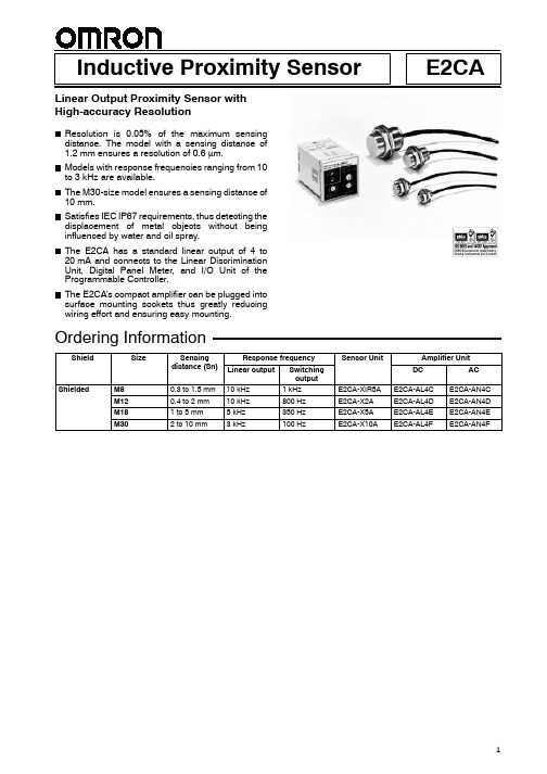
Inductive Proximity SensorE2CALinear Output Proximity Sensor withHigh-accuracy ResolutionResolution is 0.05%of the maximum sensingdistance.The model with a sensing distance of 1.2mm ensures a resolution of 0.6 m.Models with response frequencies ranging from 10to 3kHz are available.The M30-size model ensures a sensing distance of10mm.Satisfies IEC IP67requirements,thus detecting the displacement of metal objects without beinginfluenced by water and oil spray.The E2CA has a standard linear output of 4to 20mA and connects to the Linear Discrimination Unit,Digital Panel Meter,and I/O Unit of the Programmable Controller.The E2CA’s compact amplifier can be plugged into surface mounting sockets thus greatly reducing wiring effort and ensuring easy mounting.Ordering InformationShieldSizeSensing di t (S )Response frequency Sensor UnitAmplifier Unit g distance (Sn)Linear output Switchingoutput DC AC ShieldedM80.3to 1.5mm 10kHz 1kHz E2CA-XIR5A E2CA-AL4C E2CA-AN4C M120.4to 2mm 10kHz 800Hz E2CA-X2A E2CA-AL4D E2CA-AN4D M181to 5mm 5kHz 350Hz E2CA-X5A E2CA-AL4E E2CA-AN4E M302to 10mm3kHz100HzE2CA-X10A E2CA-AL4FE2CA-AN4FApplication ExamplesDetection of Metals on Other MetalsCounts the number of gear teeth.Detects mounting screws,riv-ets,and soldering conditionDetection of Loosened ScrewsImproper screwingLoosenedDiscrimination of MaterialsBrassIronCopperMeasurement of Sheet AnglesMeasures leaned press molds and elevated boardsMetal plateMeasurement of External DimensionsMetal objectAlarm outputDiscrimination of ShapesDetects top and bottom sides of metal caps and surface and back sides of nutsMeasurement of Object DeformationsE2CA Amplifier UnitE2CA Amplifier UnitE2CA Amplifier UnitE2CA Amplifier UnitE2CA Ampli-fier UnitE2CA Ampli-fier UnitE2CA Amplifier UnitE2CA Amplifier UnitE2CA Amplifier Unit OutputOutputOutputOutputOutputOutputOutputE2CAE2CA E2CA E2CA E2CAE2CAE2CA E2CAK3TS K3TSK3TSK3TS K3TS K3TSK3TS K3TSSensing Head Measurement of Sheet ThicknessSpecificationsSensor model E2CA-X1R5A E2CA-X2AItem Amplifier model E2CA-AN4C E2CA-AL4C E2CA-AN4D E2CA-AL4DSupply voltage(operating voltage range)100to240VAC50/60Hz(90to264VAC)12to24VDC(10to30VDC),ripple(p-p):10%max.100to240VAC50/60Hz(90to264VAC)12to24VDC(10to30VDC),ripple(p-p):10%max.Current consumption60mA max.70mA max.60mA max.70mA max. Sensing object Ferrous metalSensing range(with standard sensing object)0.3to1.5mm(8x8x1mm iron)0.4to2mm(12x12x1mm iron)Linear output h t i ti Resolution0.05%FSpcharacteristics Linearity 2%FS 1.5%FSResponse frequency(see note1)10kHz(--1dB)10kHz(--1dB)Switching output h t i ti Differential travel2%to5%of rated sensing distanceg pcharacteristics Response frequency(see note2)1kHz800HzSensitivity adjustment f i Sensitivity adjustment(switching output)Adjustments of switching output within sensing rangeadjust e tfunction Linear output4mA4-mA adjustment at20%of rated sensing distancecurrentadjustment20mA20-mA adjustment at rated sensing distanceOutput Linear output(see note3)4to20mA(with permissible load resistance of0to300 )Switching output100mA max.transistor photocoupler output at40VDC with max.residual voltage of2V Switching output mode Normally open or normally closed(selectable with selector on front panel)Cord length compensation3or5m(selectable with selector on front panel)Indicators POWER,SPAN(linear range),and OPER(switching output)indicatorsAmbient temperature Operating:--25 C to70 C(Sensor)and--10 C to55 C(Amplifier)with no icing Ambient humidity Operating:35%to95%(Sensor)and35%to85%(Amplifier)Temperature influence 10%FS max.of linear output current at23 C in the rated ambient operatingtemperature range of the Sensor and Amplifier UnitsVoltage influence DC power supply model: 0.5%FS max.of linear output current at a voltage between80%and120%of the rated power supply voltageAC power supply model: 0.5%FS max.of linear output current at a voltage between90%and110%of the rated power supply voltageInsulation resistance50M min.(at500VDC)between the case and current carry partsDielectric strength DC power supply model:1,000VAC(50/60Hz)for1min between current carry partsand caseAC power supply model:1,500VAC(50/60Hz)for1min between current carry partsand caseVibration resistance Sensor(destruction):10to55Hz,1.5-mm double amplitude for2hours each in X,Y,andZ directionsAmplifier(destruction):10to25Hz,2-mm double amplitude for2hours each in X,Y,andZ directionsShock resistance Sensor(destruction):500m/s2(approx.50G)3times each in X,Y,and Z directionsAmplifier(destruction):100m/s2(approx.10G)3times each in X,Y,and Z directions Degree of protection Sensor:IEC60529IP67(JEM IP67g waterproof and oil-proof)Cord length Sensor:2-conductor,3-m-long(standard length)or5-m-long shielded cordWeight (t Sensor Approx.40gg(see note4)Amplifier Approx.250g Approx.140g Approx.250g Approx.140g Material Case BrassSensing surface ABS resinCord PolyethyleneSensor model E2CA-X5A E2CA-X10AItem Amplifier model E2CA-AN4E E2CA-AL4E E2CA-AN4F E2CA-AL4FSupply voltage(operating voltage range)100to240VAC50/60Hz(90to264VAC)12to24VDC(10to30VDC),ripple(p-p):10%max.100to240VAC50/60Hz(90to264VAC)12to24VDC(10to30VDC),ripple(p-p):10%max.Current consumption60mA max.70mA max.60mA max.70mA max. Sensing object Ferrous metalSensing range(with standard sensingobject)1to5mm(18x18x1mm iron)2to10mm(30x30x1mm iron)Linear output h t i ti Resolution0.05%FSpcharacteristics Linearity 1.5%FS 2%FSResponse frequency(see note1)5kHz(--1dB)3kHz(--1dB)Switching output h t i ti Differential travel2%to5%of rated sensing distanceg pcharacteristics Response frequency(see note2)350Hz100HzSensitivity adjustment f i Sensitivity adjustment(switching output)Adjustments of switching output within sensing rangeadjust e tfunction Linear output4mA4-mA adjustment at20%of rated sensing distancecurrentadjustment20mA20-mA adjustment at rated sensing distanceOutput Linear output(see note3)4to20mA(with permissible load resistance of0to300 )Switching output100mA max.transistor photocoupler output at40VDC with max.residual voltage of2V Switching output mode Normally open or normally closed(selectable with selector on front panel)Cord length compensation3or5m(selectable with selector on front panel)Indicators POWER,SPAN(linear range),and OPER(switching output)indicatorsAmbient temperature Operating:--25 C to70 C(Sensor)and--10 C to55 C(Amplifier)with no icing Ambient humidity Operating:35%to95%(Sensor)and35%to85%(Amplifier)Temperature influence 10%FS max.of sensing distance at23 C in the rated ambient operating temperaturerange of--10 C and40 CVoltage influence DC power supply model: 0.5%FS max.of linear output current at a voltage between80%and120%of the rated power supply voltageAC power supply model: 0.5%FS max.of linear output current at a voltage between90%and110%of the rated power supply voltageInsulation resistance50M min.(at500VDC)between the case and current carry partsDielectric strength DC power supply model:1,000VAC(50/60Hz)for1min between current carry partsand caseAC power supply model:1,500VAC(50/60Hz)for1min between current carry partsand caseVibration resistance Sensor(destruction):10to55Hz,1.5-mm double amplitude for2hours each in X,Y,andZ directionsAmplifier(destruction):10to25Hz,2-mm double amplitude for2hours each in X,Y,andZ directionsShock resistance Sensor(destruction):500m/s2(approx.50G)3times each in X,Y,and Z directionsAmplifier(destruction):100m/s2(approx.10G)3times each in X,Y,and Z directions Degree of Protection Sensor:IEC60529IP67(JEM IP67g waterproof and oil-proof)Cord length Sensor:2-conductor,3-m-long(standard length)or5-m-long shielded cordWeight (t Sensor Approx.60g Approx.160gg(see note4)Amplifier Approx.250g Approx.140g Approx.250g Approx.140g Material Case BrassSensing surface ABS resinCord PolyethyleneNote: 1.This is a frequency decreasing the level of linear output current by1dB.2.This is a response frequency measured in accordance with CENELEC standards.3.The maximum load impedance of the E2CA-AL4is150 at a supply voltage of12V.4.The weight includes the3-m-long cord.The weights of the Amplifiers do not include connecting sockets.Engineering DataSensing Distance vs.Output Current (Typical)E2CA-X1R5A E2CA-X2A E2CA-X5A E2CA-X10A Sensing Object Size vs.Linearity (Typical)E2CA-X1R5A E2CA-X2A E2CA-X5A E2CA-X10A Column Diameter vs.Linearity (Typical)E2CA-X1R5A E2CA-X2A E2CA-X5A E2CA-X10A O u t p u t c u r r e n t (m A )Sensing distance (mm)O u t p u t c u r r e n t (m A )Sensing distance (mm)O u t p u t c u r r e n t (m A )Sensing distance (mm)O u t p u t c u r r e n t (m A )Sensing distance (mm)L i n e a r i t y (%o f f u l l s c a l e )Sensing distance X (mm)L i n e a r i t y (%o f f u l l s c a l e )Sensing distance X (mm)L i n e a r i t y (%o f f u l l s c a l e )Sensing distance X (mm)L i n e a r i t y (%o f f u l l s c a l e )Sensing distance X (mm)L i n e a r i t y (%o f f u l l s c a l e )Sensing distance X (mm)L i n e a r i t y (%o f f u l l s c a l e )Sensing distance X (mm)L i n e a r i t y (%o f f u l l s c a l e )Sensing distance X (mm)L i n e a r i t y (%o f f u l l s c a l e )Sensing distance X (mm)8dia.10dia.6dia.10dia.20dia.30dia.40dia.Flat plateFlat plateFlat plateFlat plateMaterial:Iron t=1140dia.220dia.Sensing object material:Iron t=1Material:Iron t=1Sensing object material:Iron t=1Sensing object material:IronSensing object material:IronMaterial:IronMaterial:Ironfff20dia.10dia.30dia.40dia.60dia.100dia.NomenclatureSelector and Adjuster Settings(1)Operation Mode SelectorThe switching output transistor turns ON when there is sensing object detection.The switching output transistor turns ON when there is no sensing object detection.POWER indicator (red LED)ON when power is supplied to the E2CA.OPER indicatorON when the switching output of the POWER indicator is detected.(ON when detected,OFF when not detected)(1)Operation mode selector(2)Cord length compensation selectorSENSITIVITY adjusterUsed to adjust the sensing distance of switching output.SPAN indicatorIndicates the linear range of green LED output current.Linear output current adjuster (20mA)Linear output current adjuster (4mA)(2)Cord Length Compensation Selector Set the selector to 3m or 5m according to the length of the Sensor cord in use.A cord length of 3m is selected.A cord length of 5m isselected.OUTPUT OUTPUT NONONCNC CABLECABLE 3m3m5m5mLinear Output Adjustment (LINEARITY Adjuster)Step 123RemarksPositioning---20%of rated sensing distanceStandard objectStandard objectRated sensing distance---LINEARITY adjuster---4mA20mA---Adjustment procedureConnect an ammeter across terminals 1and 2.Shielded cordNote:This illustration shows the Sensor Unit connected to the Amplifier Unit with the P2CF-11Front-connecting Socket mounted.P2CF-11Switching output(photocoupler output)E2CA-A j 4j Amplifier Unit P2CF-11Front-connecting SocketPlace the standard object at 20%of the rated sensing distance away from the Sensor Unit.Turn the 4mA LINEARITY adjuster slowly clockwise (the output current is increased)orcounterclockwise (the output current isdecreased)to set the output current to 4mA.(SPAN indicator is ON.)Fasten the standard object at the ratedsensing distance.Turn the 20-mA LINEARITY adjuster slowlyclockwise (the output current is increased)or counterclockwise (the output current isdecreased)to set the output current to 20mA.(SPAN indicator is ON.)To further improve the adjustment accuracy,set again theposition of the standard object in the order of steps 2and 3.Perform minute adjustment of the output current.Sensitivity (Distance)AdjustmentDetecting conditionStandard objectStandard target (See Note at below right.)SENSITIVITY adjusterSENSITIVITYLowHighAdjustment procedurePlace the standard object at the specified position.Slowly turn the SENSITIVITYadjuster clockwise (toward “High”)and stop it when the OPER.indicator illuminates.Move the object to confirm that the OPER.indicator is ON when the object is at the specified position and that it is OFF when the object is moved away from that position.Compensation of Cord Length DifferenceSet the CABLE selector to the required position according to the length of the cord being used (3m or 5m).CABLE 3m5m3-mcord CABLE 3m5m 5-m cordOperationOutput CircuitTiming ChartMain circuitCompa-rator100mA max.47VLinear output:4to 20mASwitching output (+)Switching output (--)0VDistance of objectSPAN indicatorLinear outputMode selectorTransistor output (switching output)OPER.indicator2.2100%(Rated distance)20%(Set distance)ON OFF20mA 4mAON OFFON OFF NO NC*SENSITIVITY adjusterConnectionsConnections between Sensor Units and Amplifier UnitsE2CA-AL4j +Sensor UnitSensor UnitShielded cordWhite BlueSwitching output (Transistorizedphotocoupler output)0V 12to 24VDC 0V (+)Linear outputSensor UnitShielded cordWhite BlueSwitching output (Transistorized photocoupler output)0V (+)Linear output100to 240VACE2CA-AN4j +Sensor UnitE2CA-AL4j Amplifier unitP2CF-11Front-connecting SocketE2CA/AN4j Amplifier unitP2CF-11Front-connecting SocketNote:The above illustrations show the terminal arrangement viewed from the rear of the socket,which is coupled to the Amplifier Unit.Shielded cordWhiteBlueComparator,microproces-sor,etc.Connection of Resistive Load:E2CA-AN4j +Sensor UnitConnection to Z4W-DD1CE2CA-AN4j AmplifierSynchronous sensorShielded cord4to 20mA0V+12V Blue Output Black BrownLinear output(+)100to 200VACR(see note)E2CA-AN4j Amplifier P2CF-11Front-connecting SocketWhiteBlue100mA,30VDC max.100to 240VAc,50/60HzSensor Unit (E2CA)Z4W-DD1CNote:Resistance R when E2CA-AL4is used:300 max.at 24V/150 max.at 12V Resistance R when E2CA-AN4is used:300 max.+12V0V4to 20mA 0V0VE2CA-AL4j AmplifierP2CF-11Front-connecting SocketConnection to K3TS-SD12Connection to K3TX-AD22Shielded cord Shielded cordSensor UnitSensor UnitWhiteBlue12to 24VDCK3TS WhiteBlue12to 24VDCE2CA-AL4j AmplifierP2CF-11Front-connecting SocketK3TXCQM1Linear Sensor Interface UnitConnection to CQM1-LSEShielded cord SensorE2CA-AL4j AmplifierP2CF-11Front-connecting SocketWhiteBlue4to 20mACQM1-LSE01DimensionsNote:All units are in millimeters unless otherwise indicated.Sensor UnitsE2CA-X1R5AE2CA-X2AShielded cordStandard length:3mShielded cordStandard length:3m2.8dia.2.8dia.E2CA-X5A E2CA-X10AShielded cordStandard length:3m ShieldedcordStandard length:3m5.5dia.4.1dia.Amplifier UnitsE2CA-A j C/F E2CA-Aj D/E48x 4844.8x44.8Mounting Hole DimensionsModelF (mm)E2CA-X1R5A 8.5dia.+0.50E2CA-X2A 12.5dia.+0.50E2CA-X5A 18.5dia.+0.50E2CA-X10A30.5dia.+0.50Accessories (Order Separately)Mounting Fixture (Y92E-B Series)Four types of exclusive resin mounting fixtures are optionally available.Select the type suited to the dimensions of the Sensor.Y92F-30Adapter for Flush MountingY92A-48B Protective CoverThe protective hard plastic cover shields the front panel,particularly the setting section,from dust,dirt,and water drip.Mounting panelY92F-30Adapter for flush mountingP3GA-11Back-con-necting SocketY92A-48BConnecting Sockets for E2CA-A j 4jP2CF-11Front-connecting Socket (Track Mounted)Eleven,M3.5 7.5sems screwsTwo,4.5-dia.hole70max.31.2max.Terminal Arrangement (Top View)Mounting HolesTwo,4.5-dia.holesNote:The Socket can be mounted to a track.50max.P3GA-11Back-connecting SocketTerminal Arrangement (Bottom View)27dia.454525.64.516.36.211PL11Back-connecting Socket (Solder Terminal)Terminal Arrangement (Bottom View)Mounting HolesTwo,3.5dia.or M3socket mounting holes31-dia.hole51max.35max.30dia.Approx.20.5Two,2dia.Two,3.5dia.or M3socket mounting holesPrecautionsCorrect UseMountingDo not tighten the nut of the Sensor with excessive force.Be sureto use the washer with the nut when tightening.Model Tightening torqueE2CA-X1R5A 1.96N S m (20kgf S cm)E2CA-X2A 5.9N S m (60kgf S cm)E2CA-X5A 14.7N S m (150kgf S cm)E2CA-X10A 39.2N S m (400kgf S cm)Note:The above tightening torque applies when a toothed wash-er is used.Effects of Surrounding MetalBe sure to separate the Sensor from surrounding metal objects as shown in the following illustration if the Sensor is embedded.d dia.Model/DistancedDmE2CA-X1R5A 0(8)0 4.5E2CA-X2A 0(12)06E2CA-X5A 0(18)015E2CA-X10A 0(30)30Note:The values for “d”indicate distances for the outer diameter of the shielded models.Mutual InterferenceIf the Sensors are mounted in parallel or face-to-face,be sure to keep the clearance between the Sensors as specified in the table.Model/DistanceABE2CA-X1R5A 3020E2CA-X2A3020E2CA-X5A 5035E2CA-X10A10075Sensor CordThe Sensor cord must be either 3or 5m.Do not cut or extend the Sensor cord,otherwise the E2CA may not provide the specified out-put.Mounting the Amplifier UnitWhen mounting more than one amplifier vertically,it is recom-mended that a margin of approximately 20mm above and below the Socket be provided in consideration of the space required by the hook of the Socket.HookDuctPanelP2CF-1112Enclosed MountingIf the Y92F-30Adapter is used,insert the E2CA into the square hole from the front side of the panel and slide the Y92F-30onto the E2CA from the rear side of the E2CA.Then press the Y92F-30so that the space between the Y92F-30and the panel is reduced as much as possible.Finally,secure the Y92F-30with screws.Panel Y92F-30Adapter P3G-11Back-mounting SocketRemoving the Amplifier UnitIf the Y92F-30is used,loosen the screws of theY92F-30,spread out the hooks,and remove the Y92F-30.OthersThe accuracy of the E2CA will vary with the on-site environment.The resolution,temperature characteristics,and voltage character-istic linearity are especially affected.Therefore,keep the on-site en-vironment as suitable for the E2CA as possible.OMRON CorporationIndustrial Sensors DivisionSensing Devices and Components Division H.Q.28th Fl.,Crystal Tower Bldg.1-2-27,Shiromi,Chuo-ku,Osaka 540-6028JapanPhone:(81)6-949-6012Fax:(81)6-949-6021ALL DIMENSIONS SHOWN ARE IN MILLIMETERS.To convert millimeters into inches,multiply by 0.03937.To convert grams into ounces,multiply by 0.03527.Cat.No.D77-E1-1In the interest of product improvement,specifications are subject to change without notice.Printed in Japan 0398-0.5M (0398)a。
- 1、下载文档前请自行甄别文档内容的完整性,平台不提供额外的编辑、内容补充、找答案等附加服务。
- 2、"仅部分预览"的文档,不可在线预览部分如存在完整性等问题,可反馈申请退款(可完整预览的文档不适用该条件!)。
- 3、如文档侵犯您的权益,请联系客服反馈,我们会尽快为您处理(人工客服工作时间:9:00-18:30)。
Part number EBE25RC8AAFA-5C-E EBE25RC8AAFA-4A-E EBE25RC8AAFA-4C-E
Package
Mounted devices EDE2508AASE-5C EDE2508AASE-5C, -4A EDE2508AASE-5C, -4A, -4C
Note: 1. Module /CAS latency = component CL + 1
PRELIMINARY DATA SHEET
256MB Registered DDR2 SDRAM DIMM
EBE25RC8AAFA (32M words × 72 bits, 1 Rank)
Description
The EBE25RC8AAFA is a 32M words × 72 bits, 1 rank DDR2 SDRAM Module, mounting 9 pieces of DDR2 SDRAM sealed in FBGA (µBGA) package. Read and write operations are performed at the cross points of the CK and the /CK. This high-speed data transfer is realized by the 4bits prefetch-pipelined architecture. Data strobe (DQS and /DQS) both for read and write are available for high speed and reliable data bus design. By setting extended mode register, the on-chip Delay Locked Loop (DLL) can be set enable or disable. This module provides high density mounting without utilizing surface mount technology. Decoupling capacitors are mounted beside each FBGA (µBGA) on the module board. Note: Do not push the components or drop the modules in order to avoid mechanical defects, which may result in electrical defects.
Data rate Mbps (max.) 533 400 400 Component JEDEC speed bin*1 (CL-tRCD-tRP) DDR2-533 (4-4-4) DDR2-400 (3-3-3) DDR2-400 (4-4-4) 240-pin DIMM (lead-free) Gold Contact pad
Features
• 240-pin socket type dual in line memory module (DIMM) PCB height: 30.0mm Lead pitch: 1.0mm Lead-free • 1.8V power supply • Data rate: 533Mbps/400Mbps (max.) • 1.8 V (SSTL_18 compatible) I/O • Double-data-rate architecture: two data transfers per clock cycle • Bi-directional, data strobe (DQS and /DQS) is transmitted /received with data, to be used in capturing data at the receiver • DQS is edge aligned with data for READs; center aligned with data for WRITEs • Differential clock inputs (CK and /CK) • DLL aligns DQ and DQS transitions with CK transitions • Commands entered on each positive CK edge; data referenced to both edges of DQS • Four internal banks for concurrent operation (Component) • Data mask (DM) for write data • Burst length: 4, 8 • /CAS latency (CL): 3, 4, 5 • Auto precharge option for each burst access • Auto refresh and self refresh modes • 7.8µs average periodic refresh interval • Posted CAS by programmable additive latency for better command and data bus efficiency • Off-Chip-Driver Impedance Adjustment and On-DieTermination for better signal quality • /DQS can be disabled for single-ended Data Strobe operation • 1 piece of PLL clock driver, 1 pieces of register driver and 1 piece of serial EEPROM (2k bits EEPROM) for Presence Detect (PD)
Document No. E0470E10 (Ver. 1.0) Date Published January 2004 (K) Japan URL: Elpida Memory, Inc. 2004
EBE25RC8AAFA
Ordering Information
Preliminary Data Sheet E0470E10 (Ver. 1.0)
2
EBE25RC8AAFA
Pin No. 28 29 30 31 32 33 34 35 36 37 38 39 40 41 42 43 44 45 46 47 48 49 50 51 52 53 54 55 56 57 58 59 60 Pin name DQS2 VSS DQ18 DQ19 VSS DQ24 DQ25 VSS /DQS3 DQS3 VSS DQ26 DQ27 VSS CB0 CB1 VSS /DQS8 DQS8 VSS CB2 CB3 VSS VDD CKE0 VDD NC NC VDD A11 A7 VDD A5 Pin No. 88 89 90 91 92 93 94 95 96 97 98 99 100 101 102 103 104 105 106 107 108 109 110 111 112 113 114 115 116 117 118 119 120 Pin name VSS DQ40 DQ41 VSS /DQS5 DQS5 VSS DQ42 DQ43 VSS DQ48 DQ49 VSS SA2 NC VSS /DQS6 DQS6 VSS DQ50 DQ51 VSS DQ56 DQ57 VSS /DQS7 DQS7 VSS DQ58 DQ59 VSS SDA SCL Pin No. 148 149 150 151 152 153 154 155 156 157 158 159 160 161 162 163 164 165 166 167 168 169 170 171 172 173 174 175 176 177 178 179 180 Pin name VSS DQ22 DQ23 VSS DQ28 DQ29 VSS DM3/DQS12 NU/ /DQS12 VSS DQ30 DQ31 VSS CB4 CB5 VSS DM8/DQS17 NU/ /DQS17 VSS CB6 CB7 VSS VDD NC VDD NC NC VDD A12 A9 VDD A8 A6 Pin No. 208 209 210 211 212 213 214 215 216 217 218 219 220 221 222 223 224 225 226 227 228 229 230 231 232 233 234 235 236 237 238 239 240 Pin name DQ44 DQ45 VSS DM5/DQS14 NU/ /DQS14 VSS DQ46 DQ47 VSS DQ52 DQ53 VSS NC NC VSS DM6/DQS15 NU/ /DQS15 VSS DQ54 DQ55 VSS DQ60 DQ61 VSS DM7/DQS16 NU/ /DQS16 VSS DQ62 DQ63 VSS VDDSPD SA0 SA1
Pin No. 181 182 183 184 185 186 187 188 189 190 191 192 193 194 195 196 197 198 199 200 201 202 203 204 205 206 207
Pin name VDD A3 A1 VDD CK0 /CK0 VDD A0 VDD BA1 VDD /RAS /CS0 VDD ODT0 NC VDD VSS DQ36 DQ37 VSS DM4/DQS13 NU/ /DQS13 VSS DQ38 DQ39 VSS
Pin name VREF VSS DQ0 DQ1 VSS /DQS0 DQS0 VSS DQ2 DQ3 VSS DQ8 DQ9 VSS /DQS1 DQS1 VSS /RESET NC VSS DQ10 DQ11 VSS DQ16 DQ17 V 64 65 66 67 68 69 70 71 72 73 74 75 76 77 78 79 80 81 82 83 84 85 86 87