60CPH03PBF中文资料
AP60N03S中文资料

N-CHANNEL ENHANCEMENT MODE POWER MOSFET▼ Low On-Resistance BV DSS 30V ▼ Fast SwitchingR DS(ON)13.5m Ω▼ Simple Drive RequirementI D55ADescriptionAbsolute Maximum RatingsSymbol Units V DS V V GSV I D @T C =25℃A I D @T C =100℃A I DMA P D @T C =25℃W W/℃T STG ℃T J℃Symbol Value Unit Rthj-c Thermal Resistance Junction-case Max. 2.0℃/W Rthj-aThermal Resistance Junction-ambientMax.62℃/WData & specifications subject to change without noticeThermal DataParameterStorage Temperature RangeTotal Power Dissipation 62.5-55 to 150Operating Junction Temperature Range-55 to 150Linear Derating Factor 0.5Continuous Drain Current, V GS @ 10V 35Pulsed Drain Current 1215Gate-Source VoltageContinuous Drain Current, V GS @ 10V 55ParameterRating Drain-Source Voltage 30200218032AP60N03SThe Advanced Power MOSFETs from APEC provide the designer with the best combination of fast switching,ruggedized device design, low on-resistance and cost-effectiveness.The TO-263 package is universally preferred for all commercial-industrial surface mount applications and suited for low voltage applications such as DC/DC converters. The through-hole version (AP60N03P) is available for low-profile applications.± 20G DSTO-263Electrical Characteristics@T j =25o C(unless otherwise specified)Symbol ParameterTest ConditionsMin.Typ.Max.Units BV DSSDrain-Source Breakdown VoltageV GS =0V, I D =250uA 30--V ΔB V DSS /ΔT jBreakdown Voltage Temperature Coefficient Reference to 25℃, I D =1mA-0.037-V/℃R DS(ON)Static Drain-Source On-Resistance V GS =10V, I D =28A -11.513.5m ΩV GS =4.5V, I D =22A -1820m ΩV GS(th)Gate Threshold Voltage V DS =V GS , I D =250uA 1-3V g fs Forward TransconductanceV DS =10V, I D =28A -30-S I DSS Drain-Source Leakage Current (T j =25o C)V DS =30V, V GS =0V --1uA Drain-Source Leakage Current (T j =150o C)V DS =24V, V GS =0V --25uA I GSS Gate-Source Forward Leakage V GS =--nA Q g Total Gate Charge 2I D =28A -22.4-nC Q gs Gate-Source Charge V DS =24V - 2.7-nC Q gd Gate-Drain ("Miller") Charge V GS =5V -14-nC t d(on)Turn-on Delay Time 2V DS =15V -7.4-ns t r Rise TimeI D =28A-81-ns t d(off)Turn-off Delay Time R G =3.3Ω,V GS =10V -24-ns t f Fall Time R D =0.53Ω-18-ns C iss Input Capacitance V GS =0V -950-pF C oss Output CapacitanceV DS =25V -440-pF C rssReverse Transfer Capacitancef=1.0MHz-145-pFSource-Drain DiodeSymbol ParameterTest ConditionsMin.Typ.Max.Units I S Continuous Source Current ( Body Diode )V D =V G =0V , V S =1.3V --55A I SM Pulsed Source Current ( Body Diode )1--215A V SDForward On Voltage 2T j =25℃, I S =55A, V GS =0V--1.3VNotes:1.Pulse width limited by safe operating area.2.Pulse width <300us , duty cycle <2%.AP60N03S± 20V ±100Fig 1. Typical Output Characteristics Fig 2. Typical Output CharacteristicsFig 3. On-Resistance v.s. Gate VoltageFig 4. Normalized On-Resistancev.s. Junction TemperatureFig 5. Maximum Drain Current v.s. Fig 6. Typical Power DissipationCase TemperatureFig 7. Maximum Safe Operating Area Fig 8. Effective Transient Thermal ImpedanceAP60N03SFig 9. Gate Charge Characteristics Fig 10. Typical Capacitance CharacteristicsFig 11. Forward Characteristic ofFig 12. Gate Threshold Voltage v.s.Reverse DiodeJunction TemperatureAP60N03SAP60N03SFig 13. Switching Time Circuit Fig 14. Switching Time WaveformFig 15. Gate Charge Circuit Fig 16. Gate Charge Waveform。
IR2010SPBF中文资料
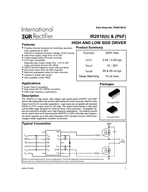
Packages
14-Lead PDIP 16-Lead SOIC
Typical Connection
200V
HO
VDD
VDD
VB
HIN
HIN
VS
SD
SD
LIN
LIN
VCC
VSS
VSS
COM
VCC
LO
(Refer to Lead Assignments for correct configuration). This/These diagram(s) show electrical connections only. Please refer to our Application Notes and DesignTips for proper circuit board layout.
元器件交易网
Data Sheet No. PD60195-D
IR2010(S) & (PbF)
Features
HIGH AND LOW SIDE DRIVER
• Floating channel designed for bootstrap operation Product Summary
Package power dissipation @ TA ≤ +25°C (14 lead DIP) (16 lead SOIC)
Thermal resistance, junction to ambient
(14 lead DIP)
(16 lead SOIC)
Junction temperature
Symbol
VB VS VHO VCC VLO VDD VSS VIN dVs/dt PD
Parker Hannifin Corporation 产品目录:D1FV 比例压力减压阀说明书

General DescriptionSeries D1FV proportional pressure reducing valves areavailable with and without onboard electronics (OBE).D1FV OBEThe digital onboard electronics is situated in a robustmetal housing, which allows the usage under roughenvironmental conditions.The nominal values are factory set. The cable forconnection to a serial RS-232 interface is available asaccessory.D1FV for External ElectronicsThe parameters can be saved, changed and dupli-cated in combination with the digital power amplifierPWD00A-400. The value parameters can be editedwith the common ProPxD software for both versions.The D1FV values control the pressure in the A- orB-ports using the barometric feedback principle.Features•Barometric feedback.• 3 command options for D1FV OBE: ±10V, 4...20mA,±20mA.•High repeatability from valve to valve.•Low hysteresis.•Manual override.•Pressure ranges 25 Bar (363 PSI) and 45 Bar (653 PSI).D1FV*3 OBED1FV D1FV OBEFunction CFunction KFunction EProportionalPressure Reducing Valve Spool TypeSize DIN NG6 CETOP 3 NFPA D031E02DPressure Range Spool PositionSolenoid Voltage 12V 2.2AKSpool / Body Design3ConnectorVSealProportional Control FDesign Series NOTE: Not required when ordering.Weight: OffboardD1FV 2.2 kg (4.9 lbs.)Code DescriptionW*Connector as per DIN 185301-803 without plug J*Connector DT04-2P "Deutsch"* Please order plugs separately. See Accessories.Please order plugs separately. See Accessories.Parametrizing cable OBE => RS-232 Item no. 409829231) Single solenoid always 0...+/-10V respectively 4...20mA.2)Factory set ± 10V on delivery.Bolt Kit:K209 (4) 10-24x1.25K375 (4) M5x30Weight: Onboard D1FV 2.9 kg (6.4 lbs.)ProportionalPressure Reducing Valve SpoolTypeSize DIN NG6 CETOP 3 NFPA D031E02DPressure Range Spool PositionInputSignalSpool / Body Design3OptionsVSealProportional Control FDesign Series NOTE: Not required when ordering.D1FV Onboard Electronics D1FV Offboard Electronics Code Input Signal 1) Function Port OptionsF00...+/-10V 0...+10V > P-A6 + PE PotentiometersupplyG00...+/-20mA 0...+20mA > P-A 6 + PE —M00...+/-10V 0...+10V > P-B6 + PE PotentiometersupplyS0 4...20mA 12...20mA > P-A 6 + PE—W5 2)0...+/-10V4...20mA 0...+/-20mA0...+10V > P-A 12...20mA > P-A 0... 20mA > P-A 11 + PE Potentiometersupply & commandpreset channelCode Description N Nitrile V FluorocarbonCode DescriptionN Nitrile V FluorocarbonWith electrical connections the protective conductor (PE W) must be connected according to the relevant regulations.Electrical SpecificationsPerformance CurvesAll performance curves measured with HLP46 at 50°C (122°F).Series D1FVBlock Diagrams — WiringCode W511 + PE acc. to EN 175201-804Code F0, M06 + PE acc. to EN 175201-804Code G0, S06 + PE acc. to EN 175201-804Series D1FV Technical Information Features• Simple editing of all parameters.• Storage and loading of optimized parameter adjustments.• Executable with all Windows ®operating systems fromWindows ®95 upwards.• Communication between PC and electronics via serialinterface RS-232.The valve electronics cannot be connected to a PC with a standard USB cable – this can result in damages of PC and/or valve electronics.Simple to use interface program. Download free of charge /euro_hcd → Services → downloadsProPxD Interface ProgramThe ProPxD software allows quick and easy setting of the digital valve electronics. Individual parameters as well as complete settings can be viewed, changed and saved via the comfortable user interface. Parameter sets saved in the non-volatile memory can be loaded to other valves of the same type or printed out for documentation purposes.The parametrizing cable may be ordered under item no. 40982923.D1FV*E D1FV*KD1FV*Cwith DT04-2P“Deutsch” Connector15.0D1FV*C OBED1FV*E OBE D1FV*K OBE。
FPA CN-60 铜镍复合金属材料规格说明书

FPA CN-60铜镍复合金属材料规格说明书Array
概述
FPA CN-60是佛山通宝精密合金股份有限公司开发的一款超薄铜镍面复合材料。
通过特殊的复合工艺,其不仅具有纯镍耐腐蚀性能,更拥有相对纯镍更优异的导电、导热特性,为锂电池的连接提供了新的解决方案。
FPA牌号:FPA CN-60
本产品铜镍比例为Ni :Cu =1:1(层厚比可基于客户要求调整)
物理性能
表1物理性能参数
外观质量
1.表面无污渍、生锈、氧化;无引起卷边的纵向凹槽;
2.横向凹痕10cm距离内不超过2处,宽度小于1/4带材宽度;
3.弯曲变形小于0.5mm/200mm;
4.无氧化、无色差;
5.凹点直径小于0.3mm,10cm内不超过2点,且表面无尖锐凸痕
6.表面划痕,肉眼应看不到划痕引起的披锋;
包装Package
1.材料内部使用白色PVC内衬
2.使用真空包装,内附干燥剂
3.包装表面标识材料信息
备注:DN系列电阻率,层厚比等指标可根据客户具体要求进行调整,欢迎垂询。
派克核电门户网站产品说明书

10 CFR 50 • AERB • ASME QME-1* • ASME QSC (NCA-3800) • ASME 第 III 部分 • ASME U核级认证核级认证 • ASN • CNSC CRN-N* HAF 604 • IAEA SC-QA 780 298* • IEEE* • ISO 9001: •E 派克核电门户网站无论您是要建新的发电厂,还是要改进现有电厂,派克都会依照行业统一的质量保证计划,使不同部门的各种产品进入核电市场,提高生产率和利润率。
这些产品包括安全专项和安全相关的核级子系统和组件,以及为非管制工厂区提供的优质的“成熟”商品。
派克门户网站是我们投入数百万美元用于核能研究和发展的承诺之一,是我们承诺提获得越来越多在全球供应且通过认证的核能产品的单一途径。
供行业所要求的高效性、可靠性和成本效益的体现。
我们支持单源购买各种产品系列,通过最新的订购方式提高工厂生产率和利润率。
另外,我们在将近 50 个国家拥有 50,000 名员工,因而门户网站产品在全球都有供应。
有关订购门户网站产品的更多信息,请:拨打电话 256 885 3833(销售)、256 885 3880(技术支持)或 发送电子邮件至 ipdusnuclear@parker .com派克核电门户网站是根据派克现行的 NQA- 1 和 10CFR50 附录 B 规定的质量保证计划开发的,并且采用了行业及规范性文件中规定的最佳实3 级阀门的 ASME N 核级认证外,派克核电门户网站上提供的产品符合 10CFR 第 21 部分中对基本组件的规定,按照认可的质保计划或是商品级物项执行。
专项不会提高质量,而是验证并记录专用项目中已有的的质量。
EU PED*HAF 604*IAEA SC-QA KTA 3507NNSANQA-1Parker Hannifin Ltd.Tachbrook Park DriveTachbrook Park,Warwick, CV34 6TU英国电话:+44 (0) 1926 317 878传真:+44 (0) 1926 317 855********************欧洲、中东和非洲AE – 阿联酋,迪拜电话:+971 4 8127100********************AT – 奥地利,维也纳新城电话:+43 (0)2622 23501-0*************************AT – 东欧,维也纳新城电话:+43 (0)2622 23501 900****************************AZ – 阿塞拜疆,巴库电话:+994 50 2233 458****************************BE/LU – 比利时,尼韦尔电话:+32 (0)67 280 900*************************BY – 白俄罗斯,明斯克电话:+375 17 209 9399*************************CH – 瑞士,埃托瓦电话:+41 (0)21 821 87 00*****************************CZ – 捷克共和国,Klecany电话:+420 284 083 111*******************************DE – 德国,卡尔斯特电话:+49 (0)2131 4016 0*************************DK – 丹麦,巴勒鲁普电话:+45 43 56 04 00*************************ES – 西班牙,马德里电话:+34 902 330 001***********************FI – 芬兰,万塔河电话:+358 (0)20 753 2500parker. ****************FR – 法国,Contamine s/Arve电话:+33 (0)4 50 25 80 25************************GR – 希腊,雅典电话:+30 210 933 6450************************HU – 匈牙利,布达佩斯电话:+36 23 885 470*************************IE – 爱尔兰,都柏林电话:+353 (0)1 466 6370*************************IT – 意大利,Corsico (MI)电话:+39 02 45 19 21***********************KZ – 哈萨克斯坦,阿拉木图电话:+7 7273 561 000****************************NL – 荷兰,奥尔登扎尔电话:+31 (0)541 585 000********************NO – 挪威,阿斯克尔电话:+47 66 75 34 00************************PL – 波兰,华沙电话:+48 (0)22 573 24 00************************PT – 葡萄牙,莱萨·达·帕尔梅拉电话:351 22 999 7360**************************RO – 罗马尼亚,布加勒斯特电话:+40 21 252 1382*************************RU – 俄罗斯,莫斯科电话:+7 495 645-2156************************SE – 瑞典,Spånga电话:+46 (0)8 59 79 50 00************************SK – 斯洛伐克,班斯卡·比斯特里察电话:+421 484 162 252**************************SL – 斯洛文尼亚,新梅斯托电话:+386 7 337 6650**************************TR – 土耳其,伊斯坦布尔电话:+90 216 4997081************************UA – 乌克兰,基辅电话:+380 44 494 2731*************************UK – 英国,沃里克电话:+44 (0)1926 317 878********************ZA – 南非,坎普顿公园电话:+27 (0)11 961 0700*****************************北美地区CA – 加拿大,安大略省米尔顿电话:+1 905 693 3000US – 美国,克利夫兰电话:+1 216 896 3000亚太地区AU – 澳大利亚,城堡山电话:+61 (0)2-9634 7777CN – 中国,上海电话:+86 21 2899 5000HK – 香港电话:+852 2428 8008IN – 印度,孟买电话:+91 22 6513 7081-85JP – 日本,东京电话:+81 (0)3 6408 3901KR – 韩国,首尔电话:+82 2 559 0400MY – 马来西亚,莎阿南电话:+60 3 7849 0800NZ – 新西兰,惠灵顿电话:+64 9 574 1744SG – 新加坡电话:+65 6887 6300TH – 泰国,曼谷电话:+662 186 7000-99TW – 台湾,台北电话:+886 2 2298 8987南美AR – 阿根廷,布宜诺斯艾利斯电话:+54 3327 44 4129BR – 巴西,圣若泽杜斯坎普电话:+55 800 727 5374CL – 智利,圣地亚哥电话:+56 2 623 1216MX – 墨西哥,阿波达卡电话:+52 81 8156 6000核电门户网站手册 M&K 12/10 1M派克授权的本地经销商© 2010 派克汉尼汾公司派克全球办事处联系信息欧洲产品信息中心免费电话:00 800 27 27 5374(AT, BE, CH, CZ, DE, DK, EE, ES, FI, FR, IE,IL, IS, IT, LU, MT, NL, NO, PL, PT, RU, SE,SK, UK, ZA)– 一点的方式。
热电偶毫伏值对照表

热电偶毫伏值对照表热电偶是一种测量温度的传感器,它可以将温度变化转换为等电位值。
热电偶是根据温度改变电阻来测量温度。
热电偶通常用来测量不同形式的温度。
热电偶毫伏值对照表是用来指导实际工作中使用热电偶时,温度值和毫伏值之间的对应关系。
热电偶的毫伏值是常见的温度检测单位,它也被称为电压单位。
热电偶毫伏值的大小受温度的影响,温度变化时,毫伏值发生变化。
热电偶毫伏值一般分为两类:一类是传统的毫伏值,另一类是温度补偿的毫伏值。
毫伏值受温度的影响,随着温度的变化而变化。
热电偶毫伏值对照表的构成一般由温度和毫伏值两个主要部分组成。
此表可以列出温度变化范围和其相应的毫伏值,以便用户可以在实际使用热电偶过程中快速找到所需的毫伏值。
通过热电偶毫伏值对照表,可以更准确地测量实际温度,从而更好地控制温度。
热电偶毫伏值对照表可以根据用户需要,设计成不同的温度范围和毫伏值。
它的设计可以根据不同的热电偶型号和使用环境,考虑温度和温度补偿毫伏值之间的关系,以便用户更准确地测量温度。
热电偶毫伏值对照表的优势在于,它可以更快地准确地测量温度,控制精度更高,而且在实际应用中,这种精度的控制有可能改善产品的性能和产品的可靠性。
另外,热电偶毫伏值对照表还能够提高计算机系统的实际运行温度,有助于计算机的散热和强度分析的应用,减少可能的故障。
热电偶的操作是一件非常复杂的工作,它需要结合热电偶毫伏值对照表的指导。
这些指导可以帮助操作者更准确地确定热电偶毫伏值,提高操作效率和实际工作效果。
不仅如此,如果能够制定出更加严格的检测标准,进一步规范热电偶毫伏值对照表的使用,也可以有效地提高热电偶测量温度的准确性和使用寿命。
总而言之,热电偶毫伏值对照表是实际应用中非常有用的一种表格,它可以帮助用户更准确地测量温度,从而更好地控制温度变化。
通过使用热电偶毫伏值对照表,可以更快地准确地测量温度,控制精度更高,从而改善产品的性能和可靠性。
ZVS,ZCS 方向功率选择 范围在5KW到100KW之间

Ultrafast diode
Ultrafast diode Ultrafast diode
60
60 30
600
600 1200
1.68
1.68 4.1
34
34 47
33
34
35
36
37
38
39
40
41
42
43
44
45
46
ZVS,ZCS 方向功率選擇 範圍在5KW到100KW之間
楊益彰( YC Yang ) 亞洲區市場開發總監 台灣威世有限公司
GLOBAL LOCATIONS
2
Broadest Line Of Discrete Semiconductors And Passive Components
3
Reference Schematic
Automotive Grade Tin Wisker Level 2 full upgrade: D-Pak, D2-Pak, TO-247
Ultrafast Rectifier HID Lighting
5EWH06FNHN3 ( 5A, 600V, D-Pak) 6EWH06FNHN3 ( 6A, 600V, D-Pak) 8EWH06FNHN3 ( 8A, 600V, D-Pak) XXXX (6-10A Fred 600V, SMPC)
Ultrafast Diodes Roadmap for Automotive
Die Technology improvements
Gen 4 Fred Pt 600V Shift down on Vf and Qrr trade off
1200V Tjmax=175°C
人民电器 三相组合式金属氧化物避雷器(TBP) 产品说明书
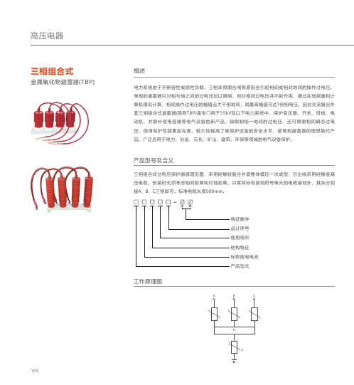
概述电力系统由于开断容性或感性负载、三相非同期合闸等原因会引起相间或相对地间的操作过电压。
常规的避雷器只对相与地之间的过电压加以限制,但对相间过电压并不起作用。
通过实地测量和计算机模似计算,相间操作过电压的幅值远大干相地间,其最高幅值可达7倍相电压。
因此交流复合外套三相组合式避雷器(简称TBP)是专门用于35kV 及以下电力系统中,保护变压器、开关、母线、电动机、并联补偿电容器等电气设备的新产品,除限制相一地间的过电压,还可限制相间瞬态过电压,使得保护性能更加完善,极大地提高了被保护设备的安全水平,是常规避雷器的理想换代产品。
广泛应用于电力、冶金、石化、矿山、建筑、环保等领域的电气设备保护。
三相组合式过电压保护器原理见图,采用硅橡胶复合外套整体模压一次成型,引出线采用硅橡胶高压电缆,安装时无须考虑相间距离和对地距离,只需将标有接地符号单元的电缆接地外,其余分别接A 、B 、C 三相即可。
标准电缆长度500mm 。
产品型号及含义特征数字设计序号使用场所结构特征标称放电电流产品型式三相组合式金属氧化物避雷器(TBP )工作原理图ABCEN高压电器165166三相组合式避雷器是针对常用避雷器的弱点设计的一种新产品,是有四组金属氧化物电阻片组成,具有其它同类产品不可比拟的特点和优点。
本产品选用阻燃、耐老化的硅橡胶做外壳材料,从内部引出四根硅橡胶高压电缆和电阻片整体一次模压硫化成型、故其电气绝缘性能好、介电强度高、抗电蚀、耐老化,而且体积小、安装方便,可根据现场情况灵活安装。
性能及优点订货时请注明以下内容:1、产品名称及型号、使用场所,如有特殊要求,请标明技术参数和具体要求。
2、若用户对安装尺寸、电缆长度、接线端子孔径有特殊要求,请注明。
3、组合式避雷器系列产品分户内、户外两种,供用户选用。
订货须知本产品可以装在各种不同型号的KYN 、CBC 、JYN 、GZSI 、XCN 等35kV 以下高压开关柜内和其它场所。
- 1、下载文档前请自行甄别文档内容的完整性,平台不提供额外的编辑、内容补充、找答案等附加服务。
- 2、"仅部分预览"的文档,不可在线预览部分如存在完整性等问题,可反馈申请退款(可完整预览的文档不适用该条件!)。
- 3、如文档侵犯您的权益,请联系客服反馈,我们会尽快为您处理(人工客服工作时间:9:00-18:30)。
Document Number: 94500For technical questions, contact: diodes-tech@Hyperfast Rectifier,2 x 30 A FRED Pt TM60CPH03PbFVishay High Power ProductsFEATURES•Ultrafast recovery time •Low forward voltage drop •Low leakage current•175 °C operating junction temperature •Lead (Pb)-free (“PbF” suffix)•Designed and qualified for industrial levelDESCRIPTIONS/APPLICATIONS60CPH03PbF series are the state of the art ultrafast recovery rectifiers designed with optimized performance of forward voltage drop and ultrafast recovery time.The planar structure and the platinum doped life time control guarantee the best overall performance, ruggedness and reliability characteristics.These devices are intended for use in the output rectification stage of SMPS, UPS, dc-to-dc converters as well as freewheeling diodes in low voltage inverters and chopper motor drives.Their extremely optimized stored charge and low recovery current minimize the switching losses and reduce over dissipation in the switching element and snubbers.PRODUCT SUMMARYt rr 55 ns I F(AV) 2 x 30 A V R300 VABSOLUTE MAXIMUM RATINGSPARAMETER SYMBOL TEST CONDITIONS MAX.UNITSRepetitive peak reverse voltage V RRM 300VAverage rectified forward currentper leg I F(AV)T C = 143 °C 30A total device60Non-repetitive peak surge current per leg I FSM T J = 25 °C300Operating junction and storage temperaturesT J , T Stg- 65 to 175°C ELECTRICAL SPECIFICATIONS (T J = 25 °C unless otherwise specified)PARAMETER SYMBOL TEST CONDITIONS MIN.TYP. MAX. UNITS Breakdown voltage,blocking voltage V BR , V R I R = 100 µA 300--VForward voltage V F I F = 30 A- 1.08 1.25I F = 30 A, T J = 125 °C -0.92 1.00Reverse leakage current I R V R = V R rated-0.0560µA T J = 125 °C, V R = V R rated -20300Junction capacitance C T V R = 300 V-70-pF Series inductanceL SMeasured lead to lead 5 mm from package body- 3.5-nH 元器件交易网 For technical questions, contact: diodes-tech@Document Number: 9450060CPH03PbFVishay High Power ProductsHyperfast Rectifier,2 x 30 A FRED Pt TMDYNAMIC RECOVERY CHARACTERISTICS (T J = 25 °C unless otherwise specified)PARAMETER SYMBOL TEST CONDITIONS MIN. TYP. MAX. UNITSReverse recovery timet rrI F = 1.0 A, dI F /dt = 50 A/µs, V R = 30 V--55nsT J = 25 °C I F = 30 AdI F /dt = - 200 A/µs V R = 200 V-39-T J = 125 °C-57-Peak recovery current I RRM T J = 25 °C - 2.8-A T J = 125 °C -7.5-Reverse recovery chargeQ rrT J = 25 °C -55-nC T J = 125 °C-214-THERMAL - MECHANICAL SPECIFICATIONSPARAMETER SYMBOL TEST CONDITIONSMIN.TYP.MAX.UNITS Maximum junction and storagetemperature range T J , T Stg- 65-175°CThermal resistance,junction to case per leg R thJC -0.50.9°C/W Thermal resistance,junction to ambient per leg R thJA Typical socket mount--40Thermal resistance, case to heatsink R thCSMounting surface, flat, smooth and greased-0.4-Weight- 6.0-g -0.22-oz.Mounting torque 6.0(5.0)-12(10)kgf ⋅ cm (lbf ⋅ in)Marking deviceCase style TO-247AC60CPH03元器件交易网Document Number: 94500For technical questions, contact: diodes-tech@60CPH03PbFHyperfast Rectifier,2 x 30 A FRED Pt TMVishay High Power ProductsFig. 1 - Typical Forward Voltage Drop CharacteristicsFig. 2 - Typical Values of Reverse Current vs.Reverse VoltageFig. 3 - Typical Junction Capacitance vs. Reverse VoltageFig. 4 - Maximum Thermal Impedance Z thJC Characteristics元器件交易网 For technical questions, contact: diodes-tech@Document Number: 9450060CPH03PbFVishay High Power ProductsHyperfast Rectifier,2 x 30 A FRED Pt TMFig. 5 - Maximum Allowable Case Temperature vs.Average Forward CurrentFig. 7 - Typical Reverse Recovery Time vs. dI F /dtFig. 6 - Forward Power Loss CharacteristicsFig. 8 - Typical Stored Charge vs. dI F /dtNote(1)Formula used: T C = T J - (Pd + Pd REV ) x R thJC ;Pd = Forward power loss = I F(AV) x V FM at (I F(AV)/D) (see fig. 6);Pd REV = Inverse power loss = V R1 x I R (1 - D); I R at V R1 = Rated V R元器件交易网Document Number: 94500For technical questions, contact: diodes-tech@60CPH03PbFHyperfast Rectifier,2 x 30 A FRED Pt TMVishay High Power ProductsFig. 9 - Reverse Recovery Parameter Test CircuitFig. 10 - Reverse Recovery Waveform and Definitions元器件交易网元器件交易网Vishay High Power Products Hyperfast Rectifier,2 x 30 A FRED Pt TMORDERING INFORMATION TABLELINKS TO RELATED DOCUMENTSDimensions /doc?95223Part marking information /doc?95226 For technical questions, contact: diodes-tech@ Document Number: 94500Disclaimer Legal Disclaimer NoticeVishayAll product specifications and data are subject to change without notice.Vishay Intertechnology, Inc., its affiliates, agents, and employees, and all persons acting on its or their behalf (collectively, “Vishay”), disclaim any and all liability for any errors, inaccuracies or incompleteness contained herein or in any other disclosure relating to any product.Vishay disclaims any and all liability arising out of the use or application of any product described herein or of any information provided herein to the maximum extent permitted by law. The product specifications do not expand or otherwise modify Vishay’s terms and conditions of purchase, including but not limited to the warranty expressed therein, which apply to these products.No license, express or implied, by estoppel or otherwise, to any intellectual property rights is granted by this document or by any conduct of Vishay.The products shown herein are not designed for use in medical, life-saving, or life-sustaining applications unless otherwise expressly indicated. Customers using or selling Vishay products not expressly indicated for use in such applications do so entirely at their own risk and agree to fully indemnify Vishay for any damages arising or resulting from such use or sale. Please contact authorized Vishay personnel to obtain written terms and conditions regarding products designed for such applications.Product names and markings noted herein may be trademarks of their respective owners.元器件交易网Document Number: 。