MAX421EWE中文资料
MAX471MAX472的中文资料大全
M A X471M A X472的中文资料大全(总4页)-本页仅作为预览文档封面,使用时请删除本页-MAX471/MAX472的特点、功能美国美信公司生产的精密高端电流检测放大器是一个系列化产品,有MAX471/MA X472、 MAX4172/MAX4173等。
它们均有一个电流输出端,可以用一个电阻来简单地实现以地为参考点的电流/电压的转换,并可工作在较宽电压内。
MAX471/MAX472具有如下特点:●具有完美的高端电流检测功能;●内含精密的内部检测电阻(MAX471);●在工作温度范围内,其精度为2%;●具有双向检测指示,可监控充电和放电状态;●内部检测电阻和检测能力为3A,并联使用时还可扩大检测电流范围;●使用外部检测电阻可任意扩展检测电流范围(MAX472);●最大电源电流为100μA;●关闭方式时的电流仅为5μA;●电压范围为3~36V;●采用8脚DIP/SO/STO三种封装形式。
MAX471/MAX472的引脚排列如图1所示,图2所示为其内部功能框图。
表1为MAX471/MAX472的引脚功能说明。
MAX471的电流增益比已预设为500μA/A,由于2kΩ的输出电阻(ROUT)可产生1V/A的转换,因此±3A时的满度值为3V.用不同的ROUT电阻可设置不同的满度电压。
但对于MAX471,其输出电压不应大于VRS+。
对于MAX472,则不能大于。
MAX471引脚图如图1所示,MAX472引脚图如图2所示。
MAX471/MAX472的引脚功能说明引脚名称功能MAX471MAX47211SHDN关闭端。
正常运用时连接到地。
当此端接高电平时,电源电流小于5μA2,3-RS+内部电流检测电阻电池(或电源端)。
“+”仅指示与SIGN输出有关的流动方向。
封装时已将2和3连在了一起-2空脚-3RG1增益电阻端。
通过增益设置电阻连接到电流检测电阻的电池端44GND地或电池负端55SIGN集电极开路逻辑输出端。
MAX4211EEUE+T中文资料

High-Side Power and Current Monitors MAX4210/MAX4211
ABSOLUTE MAXIMUM RATINGS
VCC, IN, CIN1, CIN2 to GND ....................................-0.3V to +6V RS+, RS-, INHIBIT, LE, COUT1, COUT2 to GND ...-0.3V to +30V IOUT, POUT, REF to GND ..........................-0.3V to (VCC + 0.3V) Differential Input Voltage (VRS+ - VRS-) .................................±5V Maximum Current into Any Pin..........................................±10mA Output Short-Circuit Duration to VCC or GND ........................10s Continuous Power Dissipation (TA = +70°C) 6-Pin TDFN (derate 24.4mW/°C above +70°C) ..........1951mW 8-Pin µMAX (derate 4.5mW/°C above +70°C) .............362mW 16-Pin TSSOP (derate 9.4mW/°C above +70°C) ..........754mW 16-Pin Thin QFN (derate 25mW/°C above +70°C) .....2000mW Operating Temperature Range ...........................-40°C to +85°C Junction Temperature ......................................................+150°C Storage Temperature Range .............................-65°C to +150°C Lead Temperature (soldering, 10s) .................................+300°C
MAX2021
零中频I/Q调制器/解调器1.概述MAX2021是一款低噪声、高线性度、直接上变频/下变频、正交调制/解调器,适用于手持RFID、便携式读卡器以及750MHz至1200MHz的单载波/多载波GSM/EDGE、CDMA2000®、WCDMA和iDEN®基站。
与传统的二次变频结构相比,直接变频结构可显著降低发射/接收机成本,减小系统尺寸、降低功耗。
除了高线性度和低噪声优势外,MAX2021还具备很高的集成度。
器件包括:两路匹配的无源混频器用于正交调制/解调、两路LO缓冲放大器和一路LO正交分配器。
另外,芯片还内置非平衡变压器,允许RF和LO单端输入。
作为附加功能,芯片内部还集成了基带输入匹配电路,可直接与发送DAC连接,省去了昂贵的I/Q缓冲放大器。
MAX2021采用单+5V供电,提供结构紧凑的36引脚TQFN (6mm x 6mm)封装,底部带有裸焊盘。
在-40°C至+85°C范围内确保电气特性。
2.关键特性•750MHz至1200MHz RF频率范围•可选择功率模式:通过外部电阻设置器件工作在低功耗/低性能模式•36引脚、(6mm x 6mm)、TQFN封装,提供高隔离度调制器性能:•满足4载波WCDMA的65dBc ACLR要求•OIP3典型值:+21dBm•OIP2典型值:+58dBm•OP1dB典型值:+16.7dBm•LO泄漏典型值:-32dBm•边带抑制典型值:43.5dBc•输出噪声谱密度:-174dBm/Hz•DC至550MHz基带输入可直接与DAC连接,减少了I/Q缓冲器的成本•直流耦合输入允许用户控制失调电压解调器性能:•IIP3典型值:+35.2dBm•IIP2典型值:+76dBm•IP1dB典型值:> 30dBm•转换损耗典型值:9.2dB•NF典型值:9.3dB•I/Q增益平衡:0.06dB•I/Q相位平衡:0.15°3.芯片结构3.1引脚配置/功能框图引脚说明MAX2021是专为在同相(I)和正交(Q)基带的输入在650MHz到1200MHz的RF频率范围中的上变频差。
MX421说明书

简介
这本手册讲述 MX421 高精度 GPS 袖珍天线系列之操作和按装。 MX421 GPS 和 DGPS 袖珍天线可以配用 Leica(徕卡)最新的控制显示器(Control and Display Units—CDU)或其他 NMEA0183 兼容的导航设备。当有差分改正数时,MX421 可达 到 1 米以内的精度;没有改正数时的精度是 3 米之内。
橙色
GPS 输出-
4
棕色
LPM 输入+
3
兰色
LPM 输入-
2
红色
+12 VDC
1
黑色
地线
图 4--MX421 接口电缆针头
在此: 针 1 和 2:用来接地和 12 VDC 输入 针 3 和 4:Leica 特征信息(LPM)输入口 针 5 和 6:GPS 输出至 MK40, MX420 或其他 NMEA0183 兼容设备 针 7 和 8:无联接
所提供之设备
MX421 系列传感器所提供之设备包括如下:
内容 (8 针型) MX421 MX421B
天线电缆(10 米)(8 股线) MX421 按装使用手册
货号
723240 723241 722569 723594
(10 针型) MX421-10 MX421B-10
天线电缆(15 米)(10 股线) MX421 按装使用手册
7
数椐接口与 MK40 数椐终端盒
MX421 及 MX421B 与 MK40 天线终端盒的联接如下图所示。这时,MX421 和 MX421B 之中只有三条电路是有用的:
红色----------------+12 VDC 黑色/屏蔽---------负极回路和信号地线 绿色----------------GPS 数椐+
MAX232中文资料,MAX232CPE,MAX232EPE,MAX232ECPE,规格书,MAXIM代理商,datasheet,PDF
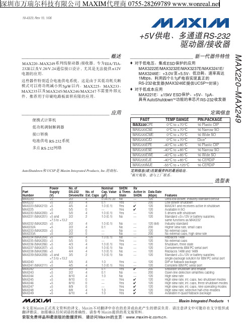
19-4323; Rev 15; 13;5V ޥ٫Ăۂ لRS-232 ഝڑಹ/ेฏಹ
________________________________ ݣะ
MAX220–MAX249࿅઼ഝڑಹ /ेฏಹLjከཛྷEIA/TIA232EჾࣆV.28/V.24ဳेਊහࣜLjᅐದกྐۨ໗ ޥ±12V ٫ᆚوᄮᅋă
ሦဗಹऔ໎Ӽคࠩ٫֠ޥ٫࿅༇Ljሦกᅑᅢದّڱߔࠞޢ ன৹ჾटࠞޢऋဏ ف5μW ჾăMAX225ĂMAX233Ă MAX235 ჾࣆ MAX245/MAX246/MAX247 ԥၖე༶ԩᆐ औLj༚ऌᅋᅢᄩฺ٫ଁғஎࢵᅘوᄮᅋă
1.0 (0.1) 0.1 — — 1.0 (0.1) — 1.0 (0.1) 1.0 (0.1) 1.0 (0.1) 1.0 (0.1)
1.0 1.0 (0.1) 0.1 0.1 1.0 — — — 1.0 1.0
SHDN & ThreeState No Yes Yes Yes Yes No
No No No No No Yes Yes No No No
_____________________________________________________________________ ၭျӹ
Part Number MAX220 MAX222 MAX223 (MAX213) MAX225 MAX230 (MAX200) MAX231 (MAX201)
MAX232 (MAX202) MAX232A MAX233 (MAX203) MAX233A MAX234 (MAX204) MAX235 (MAX205) MAX236 (MAX206) MAX237 (MAX207) MAX238 (MAX208) MAX239 (MAX209)
MAX232ECPE+中文资料

________________________________________________________________Maxim Integrated Products 1General DescriptionThe MAX202E–MAX213E, MAX232E/MAX241E line drivers/receivers are designed for RS-232 and V.28communications in harsh environments. Each transmitter output and receiver input is protected against ±15kV electrostatic discharge (ESD) shocks, without latchup.The various combinations of features are outlined in the Selector Guide.The drivers and receivers for all ten devices meet all EIA/TIA-232E and CCITT V.28specifications at data rates up to 120kbps, when loaded in accordance with the EIA/TIA-232E specification.The MAX211E/MAX213E/MAX241E are available in 28-pin SO packages, as well as a 28-pin SSOP that uses 60% less board space. The MAX202E/MAX232E come in 16-pin TSSOP, narrow SO, wide SO, and DIP packages. The MAX203E comes in a 20-pin DIP/SO package, and needs no external charge-pump capacitors. The MAX205E comes in a 24-pin wide DIP package, and also eliminates external charge-pump capacitors. The MAX206E/MAX207E/MAX208E come in 24-pin SO, SSOP, and narrow DIP packages. The MAX232E/MAX241E operate with four 1µF capacitors,while the MAX202E/MAX206E/MAX207E/MAX208E/MAX211E/MAX213E operate with four 0.1µF capacitors,further reducing cost and board space.________________________ApplicationsNotebook, Subnotebook, and Palmtop Computers Battery-Powered Equipment Hand-Held EquipmentNext-Generation Device Featureso For Low-Voltage ApplicationsMAX3222E/MAX3232E/MAX3237E/MAX3241E/MAX3246E: ±15kV ESD-Protected Down to10nA, +3.0V to +5.5V, Up to 1Mbps, True RS-232Transceivers (MAX3246E Available in a UCSP™Package)o For Low-Power ApplicationsMAX3221/MAX3223/MAX3243: 1µA SupplyCurrent, True +3V to +5.5V RS-232 Transceivers with Auto-Shutdown™o For Space-Constrained ApplicationsMAX3233E/MAX3235E: ±15kV ESD-Protected,1µA, 250kbps, +3.0V/+5.5V, Dual RS-232Transceivers with Internal Capacitorso For Low-Voltage or Data Cable ApplicationsMAX3380E/MAX3381E: +2.35V to +5.5V, 1µA,2Tx/2Rx RS-232 Transceivers with ±15kV ESD-Protected I/O and Logic PinsMAX202E–MAX213E, MAX232E/MAX241E±15kV ESD-Protected, +5V RS-232 TransceiversSelector Guide19-0175; Rev 6; 3/05Pin Configurations and Typical Operating Circuits appear at end of data sheet.YesPARTNO. OF RS-232DRIVERSNO. OF RS-232RECEIVERSRECEIVERS ACTIVE IN SHUTDOWNNO. OF EXTERNAL CAPACITORS(µF)LOW-POWER SHUTDOWNTTL TRI-STATE MAX202E 220 4 (0.1)No No MAX203E 220None No No MAX205E 550None Yes Yes MAX206E 430 4 (0.1)Yes Yes MAX207E 530 4 (0.1)No No MAX208E 440 4 (0.1)No No MAX211E 450 4 (0.1)Yes Yes MAX213E 452 4 (0.1)Yes Yes MAX232E 220 4 (1)No No MAX241E454 (1)YesFor pricing, delivery, and ordering information,please contact Maxim/Dallas Direct!at 1-888-629-4642, or visit Maxim’s website at .AutoShutdown and UCSP are trademarks of Maxim Integrated Products, Inc.Ordering InformationOrdering Information continued at end of data sheet.2_______________________________________________________________________________________M A X 202E –M A X 213E , M A X 232E /M A X 241EABSOLUTE MAXIMUM RATINGSV CC ..........................................................................-0.3V to +6V V+................................................................(V CC - 0.3V) to +14V V-............................................................................-14V to +0.3V Input VoltagesT_IN............................................................-0.3V to (V+ + 0.3V)R_IN...................................................................................±30V Output VoltagesT_OUT.................................................(V- - 0.3V) to (V+ + 0.3V)R_OUT......................................................-0.3V to (V CC + 0.3V)Short-Circuit Duration, T_OUT....................................Continuous Continuous Power Dissipation (T A = +70°C)16-Pin Plastic DIP (derate 10.53mW/°C above +70°C)....842mW 16-Pin Narrow SO (derate 8.70mW/°C above +70°C).....696mW 16-Pin Wide SO (derate 9.52mW/°C above +70°C)......762mW 16-Pin TSSOP (derate 9.4mW/°C above +70°C)...........755mW20-Pin Plastic DIP (derate 11.11mW/°C above +70°C)...889mW 20-Pin SO (derate 10.00mW/°C above +70°C).............800mW 24-Pin Narrow Plastic DIP(derate 13.33mW/°C above +70°C) ...............................1.07W 24-Pin Wide Plastic DIP(derate 14.29mW/°C above +70°C)................................1.14W 24-Pin SO (derate 11.76mW/°C above +70°C).............941mW 24-Pin SSOP (derate 8.00mW/°C above +70°C)..........640mW 28-Pin SO (derate 12.50mW/°C above +70°C)....................1W 28-Pin SSOP (derate 9.52mW/°C above +70°C)..........762mW Operating Temperature RangesMAX2_ _EC_ _.....................................................0°C to +70°C MAX2_ _EE_ _...................................................-40°C to +85°C Storage Temperature Range.............................-65°C to +165°C Lead Temperature (soldering, 10s).................................+300°CELECTRICAL CHARACTERISTICS(V CC = +5V ±10% for MAX202E/206E/208E/211E/213E/232E/241E; V CC = +5V ±5% for MAX203E/205E/207E; C1–C4 = 0.1µF for MAX202E/206E/207E/208E/211E/213E; C1–C4 = 1µF for MAX232E/241E; T A = T MIN to T MAX ; unless otherwise noted. Typical values are at T A = +25°C.)Stresses beyond those listed under “Absolute Maximum Ratings” may cause permanent damage to the device. These are stress ratings only, and functional operation of the device at these or any other conditions beyond those indicated in the operational sections of the specifications is not implied. Exposure to absolute maximum rating conditions for extended periods may affect device reliability.ELECTRICAL CHARACTERISTICS (continued)MAX202E–MAX213E, MAX232E/MAX241E (V CC= +5V ±10% for MAX202E/206E/208E/211E/213E/232E/241E; V CC= +5V ±5% for MAX203E/205E/207E; C1–C4 = 0.1µF forMAX202E/206E/207E/208E/211E/213E; C1–C4 = 1µF for MAX232E/241E; T A= T MIN to T MAX; unless otherwise noted. Typical valuesare at T A= +25°C.)Note 1:MAX211EE_ _ tested with V CC= +5V ±5%._______________________________________________________________________________________34______________________________________________________________________________________M A X 202E –M A X 213E , M A X 232E /M A X 241E__________________________________________Typical Operating Characteristics(Typical Operating Circuits, V CC = +5V, T A = +25°C, unless otherwise noted.)5.00MAX211E/MAX213ETRANSMITTER OUTPUT VOLTAGEvs. LOAD CAPACITANCELOAD CAPACITANCE (pF)V O H , -V O L (V )5.56.06.57.07.58.0100020003000400050000MAX211E/MAX213E/MAX241E TRANSMITTER SLEW RATE vs. LOAD CAPACITANCELOAD CAPACITANCE (pF)S L E W R A T E ( V /µs )5101520253010002000300040005000_______________________________________________________________________________________5MAX202E–MAX213E, MAX232E/MAX241E____________________________Typical Operating Characteristics (continued)(Typical Operating Circuits, V CC = +5V, T A = +25°C, unless otherwise noted.)2MAX202E/MAX203E/MAX232E TRANSMITTER SLEW RATE vs. LOAD CAPACITANCELOAD CAPACITANCE (pF)S L E W R A T E ( V /µs )468101214100020003000400050005.07.5-7.53000MAX205E–MAX208ETRANSMITTER OUTPUT VOLTAGEvs. LOAD CAPACITANCE-5.02.5LOAD CAPACITANCE (pF)O U T P U T V O L T A G E (V )10002000400050000-2.54550203000MAX205E–MAX208E SUPPLY CURRENT vs. LOAD CAPACITANCE2540LOAD CAPACITANCE (pF)S U P P L Y C U R R E N T (m A )100020004000500035302.55.0-10.0180MAX205E –MAX208EOUTPUT VOLTAGE vs. DATA RATE-7.50DATA RATE (kbps)O U T P U T V O L T A G E (V )601202401503090210-2.5-5.010.07.56_______________________________________________________________________________________M A X 202E –M A X 213E , M A X 232E /M A X 241EMAX203EMAX205E_____________________________________________________________Pin DescriptionsMAX202E/MAX232E_______________________________________________________________________________________7MAX202E–MAX213E, MAX232E/MAX241EMAX208E________________________________________________Pin Descriptions (continued)MAX206EMAX207E8_______________________________________________________________________________________M A X 202E –M A X 213E , M A X 232E /M A X 241EMAX211E/MAX213E/MAX241E)(MAX205E/MAX206E/MAX211E/MAX213E/MAX241E)________________________________________________Pin Descriptions (continued)MAX211E/MAX213E/MAX241EFigure 3. Transition Slew-Rate Circuit_______________Detailed Description The MAX202E–MAX213E, MAX232E/MAX241E consist of three sections: charge-pump voltage converters, drivers (transmitters), and receivers. These E versions provide extra protection against ESD. They survive ±15kV discharges to the RS-232 inputs and outputs, tested using the Human Body Model. When tested according to IEC1000-4-2, they survive ±8kV contact-discharges and ±15kV air-gap discharges. The rugged E versions are intended for use in harsh environments or applications where the RS-232 connection is frequently changed (such as notebook computers). The standard (non-“E”) MAX202, MAX203, MAX205–MAX208, MAX211, MAX213, MAX232, and MAX241 are recommended for applications where cost is critical.+5V to ±10V Dual Charge-PumpVoltage Converter The +5V to ±10V conversion is performed by dual charge-pump voltage converters (Figure 4). The first charge-pump converter uses capacitor C1 to double the +5V into +10V, storing the +10V on the output filter capacitor, C3. The second uses C2 to invert the +10V into -10V, storing the -10V on the V- output filter capacitor, C4.In shutdown mode, V+ is internally connected to V CC by a 1kΩpull-down resistor, and V- is internally connected to ground by a 1kΩpull up resistor.RS-232 Drivers With V CC= 5V, the typical driver output voltage swing is ±8V when loaded with a nominal 5kΩRS-232 receiver. The output swing is guaranteed to meet EIA/TIA-232E and V.28 specifications that call for ±5V minimum output levels under worst-case conditions. These include a 3kΩload, minimum V CC, and maximum operating temperature. The open-circuit output voltage swings from (V+ - 0.6V) to V-.Input thresholds are CMOS/TTL compatible. The unused drivers’ inputs on the MAX205E–MAX208E, MAX211E, MAX213E, and MAX241E can be left unconnected because 400kΩpull up resistors to V CC are included on-chip. Since all drivers invert, the pull up resistors force the unused drivers’ outputs low. The MAX202E, MAX203E, and MAX232E do not have pull up resistors on the transmitter inputs._______________________________________________________________________________________9MAX202E–MAX213E, MAX232E/MAX241E10______________________________________________________________________________________M A X 202E –M A X 213E , M A X 232E /M A X 241E±15kV ESD-Protected, +5V RS-232 Transceivers When in low-power shutdown mode, the MAX205E/MAX206E/MAX211E/MAX213E/MAX241E driver outputs are turned off and draw only leakage currents—even if they are back-driven with voltages between 0V and 12V. Below -0.5V in shutdown, the transmitter output is diode-clamped to ground with a 1k Ωseries impedance.RS-232 ReceiversThe receivers convert the RS-232 signals to CMOS-logic output levels. The guaranteed 0.8V and 2.4V receiver input thresholds are significantly tighter than the ±3V thresholds required by the EIA/TIA-232E specification.This allows the receiver inputs to respond to TTL/CMOS-logic levels, as well as RS-232 levels.The guaranteed 0.8V input low threshold ensures that receivers shorted to ground have a logic 1 output. The 5k Ωinput resistance to ground ensures that a receiver with its input left open will also have a logic 1 output. Receiver inputs have approximately 0.5V hysteresis.This provides clean output transitions, even with slow rise/fall-time signals with moderate amounts of noise and ringing.In shutdown, the MAX213E’s R4 and R5 receivers have no hysteresis.Shutdown and Enable Control (MAX205E/MAX206E/MAX211E/MAX213E/MAX241E)In shutdown mode, the charge pumps are turned off,V+ is pulled down to V CC , V- is pulled to ground, and the transmitter outputs are disabled. This reduces supply current typically to 1µA (15µA for the MAX213E).The time required to exit shutdown is under 1ms, as shown in Figure 5.ReceiversAll MAX213E receivers, except R4 and R5, are put into a high-impedance state in shutdown mode (see Tables 1a and 1b). The MAX213E’s R4 and R5 receivers still function in shutdown mode. These two awake-in-shutdown receivers can monitor external activity while maintaining minimal power consumption.The enable control is used to put the receiver outputs into a high-impedance state, to allow wire-OR connection of two EIA/TIA-232E ports (or ports of different types) at the UART. It has no effect on the RS-232 drivers or the charge pumps.N ote: The enabl e control pin is active l ow for the MAX211E/MAX241E (EN ), but is active high for the MAX213E (EN). The shutdown control pin is active high for the MAX205E/MAX206E/MAX211E/MAX241E (SHDN), but is active low for the MAX213E (SHDN ).Figure 4. Charge-Pump DiagramMAX202E–MAX213E, MAX232E/MAX241EV+V-200µs/div3V 0V 10V 5V 0V -5V -10VSHDNMAX211EFigure 5. MAX211E V+ and V- when Exiting Shutdown (0.1µF capacitors)X = Don't care.*Active = active with reduced performanceSHDN E N OPERATION STATUS Tx Rx 00Normal Operation All Active All Active 01Normal Operation All Active All High-Z 1XShutdownAll High-ZAll High-ZTable 1a. MAX205E/MAX206E/MAX211E/MAX241E Control Pin ConfigurationsTable 1b. MAX213E Control Pin ConfigurationsThe MAX213E’s receiver propagation delay is typically 0.5µs in normal operation. In shutdown mode,propagation delay increases to 4µs for both rising and falling transitions. The MAX213E’s receiver inputs have approximately 0.5V hysteresis, except in shutdown,when receivers R4 and R5 have no hysteresis.When entering shutdown with receivers active, R4 and R5 are not valid until 80µs after SHDN is driven low.When coming out of shutdown, all receiver outputs are invalid until the charge pumps reach nominal voltage levels (less than 2ms when using 0.1µF capacitors).±15kV ESD ProtectionAs with all Maxim devices, ESD-protection structures are incorporated on all pins to protect against electrostatic discharges encountered during handling and assembly. The driver outputs and receiver inputs have extra protection against static electricity. Maxim’s engineers developed state-of-the-art structures to protect these pins against ESD of ±15kV without damage. The ESD structures withstand high ESD in all states: normal operation, shutdown, and powered down. After an ESD event, Maxim’s E versions keep working without latchup, whereas competing RS-232products can latch and must be powered down to remove latchup.ESD protection can be tested in various ways; the transmitter outputs and receiver inputs of this product family are characterized for protection to the following limits:1)±15kV using the Human Body Model2)±8kV using the contact-discharge method specifiedin IEC1000-4-23)±15kV using IEC1000-4-2’s air-gap method.ESD Test ConditionsESD performance depends on a variety of conditions.Contact Maxim for a reliability report that documents test set-up, test methodology, and test results.Human Body ModelFigure 6a shows the Human Body Model, and Figure 6b shows the current waveform it generates when discharged into a low impedance. This model consists of a 100pF capacitor charged to the ESD voltage of interest, which is then discharged into the test device through a 1.5k Ωresistor.S H D N ENOPERATION STATUS Tx 1–400Shutdown All High-Z 01Shutdown All High-Z 10Normal Operation 11Normal OperationAll ActiveAll Active Active1–34, 5High-Z ActiveHigh-Z High-Z High-Z Active*High-Z RxM A X 202E –M A X 213E , M A X 232E /M A X 241EIEC1000-4-2The IEC1000-4-2 standard covers ESD testing and performance of finished equipment; it does not specifically refer to integrated circuits. The MAX202E/MAX203E–MAX213E, MAX232E/MAX241E help you design equipment that meets level 4 (the highest level) of IEC1000-4-2, without the need for additional ESD-protection components.The major difference between tests done using the Human Body Model and IEC1000-4-2 is higher peak current in IEC1000-4-2, because series resistance is lower in the IEC1000-4-2 model. Hence, the ESD withstand voltage measured to IEC1000-4-2 is generally lower than that measured using the Human Body Model. Figure 7b shows the current waveform for the 8kV IEC1000-4-2 level-four ESD contact-discharge test.The air-gap test involves approaching the device with a charged probe. The contact-discharge method connects the probe to the device before the probe is energized.Machine ModelThe Machine Model for ESD tests all pins using a 200pF storage capacitor and zero discharge resistance. Its objective is to emulate the stress caused by contact that occurs with handling and assembly during manufacturing. Of course, all pins require this protection during manufacturing, not just RS-232 inputs and outputs. Therefore,after PC board assembly,theMachine Model is less relevant to I/O ports.Figure 7a. IEC1000-4-2 ESD Test ModelFigure 7b. IEC1000-4-2 ESD Generator Current WaveformFigure 6a. Human Body ESD Test ModelFigure 6b. Human Body Model Current Waveform__________Applications InformationCapacitor Selection The capacitor type used for C1–C4 is not critical for proper operation. The MAX202E, MAX206–MAX208E, MAX211E, and MAX213E require 0.1µF capacitors, and the MAX232E and MAX241E require 1µF capacitors, although in all cases capacitors up to 10µF can be used without harm. Ceramic, aluminum-electrolytic, or tantalum capacitors are suggested for the 1µF capacitors, and ceramic dielectrics are suggested for the 0.1µF capacitors. When using the minimum recommended capacitor values, make sure the capacitance value does not degrade excessively as the operating temperature varies. If in doubt, use capacitors with a larger (e.g., 2x) nominal value. The capacitors’ effective series resistance (ESR), which usually rises at low temperatures, influences the amount of ripple on V+ and V-.Use larger capacitors (up to 10µF) to reduce the output impedance at V+ and V-. This can be useful when “stealing” power from V+ or from V-. The MAX203E and MAX205E have internal charge-pump capacitors. Bypass V CC to ground with at least 0.1µF. In applications sensitive to power-supply noise generated by the charge pumps, decouple V CC to ground with a capacitor the same size as (or larger than) the charge-pump capacitors (C1–C4).V+ and V- as Power Supplies A small amount of power can be drawn from V+ and V-, although this will reduce both driver output swing and noise margins. Increasing the value of the charge-pump capacitors (up to 10µF) helps maintain performance when power is drawn from V+ or V-.Driving Multiple Receivers Each transmitter is designed to drive a single receiver. Transmitters can be paralleled to drive multiple receivers.Driver Outputs when Exiting Shutdown The driver outputs display no ringing or undesirable transients as they come out of shutdown.High Data Rates These transceivers maintain the RS-232 ±5.0V minimum driver output voltages at data rates of over 120kbps. For data rates above 120kbps, refer to the Transmitter Output Voltage vs. Load Capacitance graphs in the Typical Operating Characteristics. Communication at these high rates is easier if the capacitive loads on the transmitters are small; i.e., short cables are best.Table 2. Summary of EIA/TIA-232E, V.28 SpecificationsMAX202E–MAX213E, MAX232E/MAX241EM A X 202E –M A X 213E , M A X 232E /M A X 241E____________Pin Configurations and Typical Operating Circuits (continued)Table 3. DB9 Cable ConnectionsCommonly Used for EIA/TIAE-232E and V.24 Asynchronous Interfaces____________Pin Configurations and Typical Operating Circuits (continued)MAX202E–MAX213E, MAX232E/MAX241EM A X 202E –M A X 213E , M A X 232E /M A X 241E____________Pin Configurations and Typical Operating Circuits (continued)MAX202E–MAX213E, MAX232E/MAX241E____________Pin Configurations and Typical Operating Circuits (continued)M A X 202E –M A X 213E , M A X 232E /M A X 241E____________Pin Configurations and Typical Operating Circuits (continued)MAX202E–MAX213E, MAX232E/MAX241E____________Pin Configurations and Typical Operating Circuits (continued)M A X 202E –M A X 213E , M A X 232E /M A X 241E____________Pin Configurations and Typical Operating Circuits (continued)______________________________________________________________________________________21MAX202E–MAX213E, MAX232E/MAX241E Ordering Information (continued)*Dice are specified at T A= +25°C.M A X 202E –M A X 213E , M A X 232E /M A X 241E22________________________________________________________________________________________________________________________________________________Chip Topographies___________________Chip InformationC1-V+C1+V CC R2INT2OUT R2OUT0.117"(2.972mm)0.080"(2.032mm)V-C2+ C2-T2IN T1OUT R1INR1OUT T1INGNDR5INV-C2-C2+C1-V+C1+V CC T4OUTR3IN T3OUTT1OUT 0.174"(4.420mm)0.188"(4.775mm)T4IN R5OUT R4OUT T3IN R4IN EN (EN) SHDN (SHDN)R3OUT T2OUT GNDR1IN R1OUT T2IN R2OUTR2IN T1IN ( ) ARE FOR MAX213E ONLYTRANSISTOR COUNT: 123SUBSTRATE CONNECTED TO GNDTRANSISTOR COUNT: 542SUBSTRATE CONNECTED TO GNDMAX202E/MAX232EMAX211E/MAX213E/MAX241EMAX205E/MAX206E/MAX207E/MAX208E TRANSISTOR COUNT: 328SUBSTRATE CONNECTED TO GNDMAX202E–MAX213E, MAX232E/MAX241E Package InformationM A X 202E –M A X 213E , M A X 232E /M A X 241EPackage Information (continued)MAX202E–MAX213E, MAX232E/MAX241E±15kV ESD-Protected, +5V RS-232 TransceiversMaxim cannot assume responsibility for use of any circuitry other than circuitry entirely embodied in a Maxim product. No circuit patent licenses are implied. Maxim reserves the right to change the circuitry and specifications without notice at any time.Maxim Integrated Products, 120 San Gabriel Drive, Sunnyvale, CA 94086 408-737-7600 ____________________25©2005 Maxim Integrated ProductsPrinted USAis a registered trademark of Maxim Integrated Products, Inc.Package Information (continued)(The package drawing(s) in this data sheet may not reflect the most current specifications. For the latest package outline information go to /packages .)。
MAX4211EEVKIT中文资料
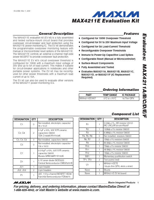
General DescriptionThe MAX4211E evaluation kit (EV kit) is a fully assembled and tested surface-mount circuit board that provides overpower circuit-breaker and fault protection using the MAX4211E power-monitoring IC. The EV kit demonstrates the programmable overpower monitoring feature with manual or microcontroller reset options of the MAX4211E.The MAX4211E controls an external p-channel high-side power MOSFET to provide overpower fault protection.The MAX4211E EV kit’s circuit overpower threshold is configured for 100W with a maximum input voltage of 20V and up to 5A of load current. This makes it suitable for circuit-breaker applications in notebooks and other portable power systems. The EV kit may be reconfig-ured for other power thresholds with a maximum load current of up to 10A.The EV kit can also be used to evaluate other versions of the MAX4211 power-monitoring ICs.Featureso Configured for 100W Overpower Threshold o Configured for 5V to 20V Maximum Input Voltage o Configured for 5A Load-Current Threshold o Reconfigurable Overpower Thresholds o Immune to Power-Up Capacitive Load Spikes o Configurable Reset (Manual or Microcontroller)o Surface-Mount Components o Fully Assembled and Testedo Evaluates MAX4211A, MAX4211B, MAX4211C,MAX4211D, or MAX4211F (IC Replacement Required)Evaluates: MAX4211A/B/C/D/E/FMAX4211E Evaluation Kit________________________________________________________________Maxim Integrated Products 119-3399; Rev 1; 3/05For pricing, delivery, and ordering information,please contact Maxim/Dallas Direct!at 1-888-629-4642, or visit Maxim’s website at .Ordering InformationComponent ListE v a l u a t e s : M A X 4211A /B /C /D /E /FQuick StartThe MAX4211E EV kit is fully assembled and tested.Follow these steps to verify board operation. Do not turn on the power supply until all connections are completed.Recommended Equipment•0 to 20V power supply capable of providing up to 5A •5V power supply•Electronic load capable of sinking up to 5A (e.g.,HP 6060B)Procedures1)Verify that a shunt is installed across pins 2 and 3 ofjumper JU1.2)Verify that shunts are installed on jumpers J U2and JU3.3)Set the 0 to 20V power supply to 10V and disablethe output.4)Connect the positive terminal of the 0 to 20V DCpower supply to the VSOURCE pad on the EV kit board. Connect the ground of this power supply to the GND pad located above the VSOURCE pads.5)Connect a voltmeter across the VSOURCE andGND pads.6)Connect the positive terminal of the 5A DC electroniccurrent load to the LOAD pad on the EV kit board.Connect the ground terminal of the electronic load to the GND pad located above the LOAD pad on the EV kit.7)Connect the positive terminal of the 5V DC powersupply to the VCC pad. Connect the ground of this power supply to the GND pad located below the VCC pad on the EV kit board.8)Connect a voltmeter across the LOAD and GNDpads on the EV kit board.9)Connect a voltmeter across the TP2 test point andGND pad.10)Turn on the 5V power supply.11)Enable the 0 to 20V (10V) power supply.12)Turn on the electronic current load.13)Verify that the voltmeter connected across theLOAD and GND pads measures 10V.14)Verify that the voltmeter connected at test point TP2measures approximately 1.25V.15)Gradually increase the VSOURCE power supplytowards 20V to cause an overpower fault,16)After the fault, verify that the voltmeter connectedacross the LOAD and GND pads measures 0V.17)Verify that the voltmeter connected at TP2 mea-sures 0V.18)Reduce V SOURCE to 10V and then reset the circuit bymomentarily pressing pushbutton SW1. Verify that the voltmeter connected at TP2 measures approximately 1.25V and LOAD voltage returns to 10V.Detailed DescriptionThe MAX4211E EV kit is a power-monitoring, circuit-breaker circuit that safeguards the supply source against excessive power dissipation due to overvoltage,overcurrent, or short-circuit conditions at the output. The circuit uses the MAX4211E power-monitoring IC that operates with a V CC voltage range of 2.7V to 5.5V.MAX4211E Evaluation Kit 2_______________________________________________________________________________________The load can be supplied through an independent sup-ply source connected across the VSOURCE and GND pads and can range from 5V to 20V. The MAX4211E controls an external high-side p-channel power MOSFET switch that disconnects the supply source from the load under overpower fault conditions.During normal operation, the EV kit circuit continually monitors the power delivered to the load. When the power delivered to the load exceeds the configured maximum power threshold, the circuit disconnects the supply source from the load thus providing overpower fault pro-tection. The EV kit can be reset to normal operation by first removing the fault condition and then momentarily pressing pushbutton SW1. The EV kit is configured for a power threshold of 100W with an input source voltage threshold of 20V and load-current threshold of 5A. The MAX4211E EV kit can be reconfigured to monitor up to 10A of current.Input Voltages The MAX4211E EV kit provides the flexibility of having independent power-supply sources for the IC and the load. The EV kit is configured for a maximum V SOURCE of 20V and a V CC of 5V. To reconfigure the EV kit’s V SOURCE maximum input voltage for up to 28V, see the Overpower Threshold section. Set the V CC voltage in the range of 2.7V to 5.5V.Overpower Threshold The overpower threshold for the MAX4211E EV kit is set to 100W with a maximum V SOURCE input voltage of 20V and maximum load current of 5A. During normal opera-tion, the EV kit circuit continually monitors the power delivered to the load. When the power delivered to the load exceeds the 100W threshold (after exceeding the 20V and 5A thresholds), the MAX4211E disconnects the supply source from the load. This is done by switching MOSFET P1 off when the MAX4211E COUT1 pin latches high.To reconfigure the MAX4211E EV kit for a different overpower threshold, the V SOURCE and load-current thresholds must be modified. Reconfigure the V SOURCE voltage threshold for up to 28V by selecting new resis-tor values for R2 and R3 using the following equation: R2 = R3 x (V SOURCE_THRESHOLD- 1)where resistor R3 is typically 6.98kΩand the V SOURCE_THRESHOLD is the new desired value. This step ensures that the MAX4211E POUT pin is 2.5V when the maximum power is delivered to the load.The MAX4211E EV kit board is configured for a load-current threshold of 5A DC, however, the 2oz PC board traces can handle up to 10A. Use the following equa-tion to select a new value for current-sense resistor R1 (2512 case):Verify that the resistor R1 and MOSFET P1 are rated for the new current level.Reset During an overpower fault condition, the MAX4211E EV kit circuit latches off. To reset the circuit, remove the fault condition and momentarily press the pushbutton switch SW1. This clears the latched COUT1 pin on the MAX4211E.The MAX4211E EV kit circuit reset function can also be controlled by connecting a microcontroller’s output across the CIN2- and GND pads and configuring jumpers J U1, J U2, and J U3. See Table1 for jumperconfiguration. Evaluates: MAX4211A/B/C/D/E/F MAX4211E Evaluation KitE v a l u a t e s : M A X 4211A /B /C /D /E /FInternal ComparatorsThe MAX4211E features two internal comparators. In the EV kit, circuit Comparator1 is used to detect over-power conditions. Comparator2 is disabled but can be configured for microcontroller reset or other comparator applications. To access CIN2+ of Comparator2,remove the shunt across J U3 and connect to pin 2 of J U3. To access CIN2-, remove the shunt across J U2and connect to the CIN2- pad. The Comparator2 output can be accessed through pin 1 of JU1. CIN2+ can be left connected to REF through JU3 or can be accessed directly through pin 2 of jumper JU3.Power-UpTransient surges in power may result when the EV kit is powered up with a capacitive load connected to the out-put (either C5 on the MAX4211E EV kit or to the LOAD PC board pad output). These transient conditions may be detected as an overpower condition and prevent MOSFET P1 from turning on. Though these transients might not always be sufficient to trip the circuit-breaker function, the MAX4211E possesses an INHIBIT circuit,which can prevent such transients from being registered as overpower conditions.The MAX4211E EV kit features an RC network consist-ing of resistors R6 and capacitor C7 that connects the LOAD node to INHIBIT of the MAX4211E. During power-up, this RC network disables the internal com-parator providing immunity against transient events for a period given by the equation:where ∆V is the voltage change at the LOAD during power-up or due to switching between different voltage sources.The MAX4211E EV kit comes configured with t INHIBIT approximately equal to 425µs, for an expected ∆V =10V and a LOAD voltage settling time of 42.5µs. For some applications, this value might be too short to sus-pend the Comparator1 operation as power-up tran-sients could be much slower. To adjust the inhibit time,select a value of t INHIBIT that is larger than the settling time (t LOAD ) of the LOAD voltage. Selecting t INHIBIT =10 x t LOAD , where t LOAD is the time constant of rising voltage at V LOAD during power-up, is a good design criterion. Larger t INHIBIT times will reduce the number of false circuit-breaker trips, but can potentially subject V SOURCE to longer periods of exposure to momentary overpower conditions.Also note that resistor R7 is merely an isolation resistor with a value that does not affect t INHIBIT.Evaluating the MAX4211A/B/C/D/FThe MAX4211E EV kit can also evaluate other versions of the MAX4211 power-monitoring IC. The MAX4211E IC must be removed and replaced with the desired IC.Refer to the MAX4210/MAX4211 IC data sheet for detailed information about the MAX4211 parts.Depending upon your version of the MAX4211, some ofthe external components may need replacement.MAX4211E Evaluation Kit 4_______________________________________________________________________________________Evaluates: MAX4211A/B/C/D/E/F MAX4211E Evaluation Kit Figure 1. MAX4211E EV Kit Schematic_______________________________________________________________________________________5Maxim cannot assume responsib ility for use of any circuitry other than circuitry entirely emb odied in a Maxim product. No circuit patent licenses are implied. Maxim reserves the right to change the circuitry and specifications without notice at any time.6_____________________Maxim Integrated Products, 120 San Gabriel Drive, Sunnyvale, CA 94086 408-737-7600©2005 Maxim Integrated ProductsPrinted USAis a registered trademark of Maxim Integrated Products, Inc.E v a l u a t e s : M A X 4211A /B /C /D /E /FMAX4211E Evaluation Kit Figure 2. MAX4211E EV Kit Component Placement Guide—Component Side Figure 3. MAX4211E EV Kit PC Board Layout—ComponentSideFigure 4. MAX4211E EV Kit PC Board Layout—Solder Side。
MAX333AEWP中文资料

________________________________________________________________ Maxim Integrated Products
1
For free samples & the latest literature: , or phone 1-800-998-8800. For small orders, phone 1-800-835-8769.
元器件交易网
Precision, Quad, SPDT, CMOS Analog Switch MAX333A
ABSOLUTE MAXIMUM RATINGS
V+ to V- ..................................................................................44V VIN, VCOM, VNO, VNC ......................................................V- to V+ (VNO - VNC) ............................................................................32V V+ to Ground..........................................................................30V V- to Ground..........................................................................-30V Current, Any Terminal Except VCOM, VNO, or VNC .............30mA Continuous Current, VCOM, VNO, or VNC ............................20mA Peak Current, VCOM, VNO, or VNC (Pulsed at 1ms, 10% duty cycle max) ............................70mA ESD ....................................................................................2000V Note 1: Device mounted with all leads soldered to PC board. Continuous Power Dissipation (TA = +70°C) (Note 1) Plastic DIP (derate above +70°C by 11.11mW/°C) .....889mW SO (derate above +70°C by 10.00mW/°C) ..................800mW CERDIP (derate above +70°C by 11.11mW/°C) ..........889mW TSSOP (derate above +70°C by 7mW/°C) ..................559mW Operating Temperature Ranges: MAX333AC_ _ .....................................................0°C to +70°C MAX333AE_ _ ..................................................-40°C to +85°C MAX333AMJP ................................................-55°C to +125°C Storage Temperature Range .............................-65°C to +150°C Lead Temperature (soldering, 10sec) .............................+300°C