MAX5231AEEE+中文资料
EEEHP1A100R中文资料(panasonic)中文数据手册「EasyDatasheet - 矽搜」
61
0.50 EEEHB0G101R
82
0.50 EEEHB0G151P
82
0.50 EEEHB0G221P
26
0.30 EEEHB0J220R
29
0.30 EEEHB0J330R
46
0.30 EEEHB0J470R
71
0.30 EEEHB0J101P
150
0.35 EEEHB0J221P
230
0.35 EEEHB0J331P
00 Nov. 2012
芯片中文手册,看全文,戳
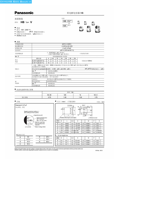
铝电解电容器/ HB
■ 标准产品
W.V.
Cap. (±20 %)
机箱尺寸
Dia. 长度
尺寸 代码
(V) (µF) 47
(毫米) (毫米)
4
5.8
B
100
5
5.8
C
4
150
6.3
5.8
D
220
6.3
5.8
D
22
4
5.8
B
33
4
5.8
B
500
(2)
500
Design and specifications are each subject to change without notice. Ask factory for the current technical specifications before purchase and/or use. Should a safety concern arise regarding this product, please be sure to contact us immediately.DΒιβλιοθήκη 25478
MAX232中文资料,MAX232CPE,MAX232EPE,MAX232ECPE,规格书,MAXIM代理商,datasheet,PDF
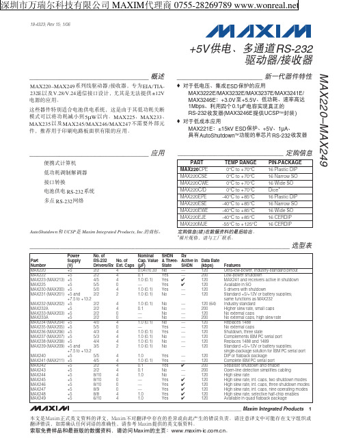
19-4323; Rev 15; 13;5V ޥ٫Ăۂ لRS-232 ഝڑಹ/ेฏಹ
________________________________ ݣะ
MAX220–MAX249࿅઼ഝڑಹ /ेฏಹLjከཛྷEIA/TIA232EჾࣆV.28/V.24ဳेਊහࣜLjᅐದกྐۨ໗ ޥ±12V ٫ᆚوᄮᅋă
ሦဗಹऔ໎Ӽคࠩ٫֠ޥ٫࿅༇Ljሦกᅑᅢದّڱߔࠞޢ ன৹ჾटࠞޢऋဏ ف5μW ჾăMAX225ĂMAX233Ă MAX235 ჾࣆ MAX245/MAX246/MAX247 ԥၖე༶ԩᆐ औLj༚ऌᅋᅢᄩฺ٫ଁғஎࢵᅘوᄮᅋă
1.0 (0.1) 0.1 — — 1.0 (0.1) — 1.0 (0.1) 1.0 (0.1) 1.0 (0.1) 1.0 (0.1)
1.0 1.0 (0.1) 0.1 0.1 1.0 — — — 1.0 1.0
SHDN & ThreeState No Yes Yes Yes Yes No
No No No No No Yes Yes No No No
_____________________________________________________________________ ၭျӹ
Part Number MAX220 MAX222 MAX223 (MAX213) MAX225 MAX230 (MAX200) MAX231 (MAX201)
MAX232 (MAX202) MAX232A MAX233 (MAX203) MAX233A MAX234 (MAX204) MAX235 (MAX205) MAX236 (MAX206) MAX237 (MAX207) MAX238 (MAX208) MAX239 (MAX209)
MAX3232EEAE+T中文资料

Battery-Powered Equipment Cell Phones Cell-Phone Data Cables Notebook, Subnotebook, and Palmtop Computers
Applications
Printers Smart Phones xDSL Modems
MAX3222EEPN -40°C to +85°C 18 Plastic DIP —
MAX3232ECAE 0°C to +70°C 16 SSOP
—
MAX485EEPA+中文资料

14-Pin Plastic DIP (derate 10.00mW/°C above +70°C) ..800mW 8-Pin SO (derate 5.88mW/°C above +70°C).................471mW 14-Pin SO (derate 8.33mW/°C above +70°C)...............667mW Operating Temperature Ranges MAX4_ _C_ _/MAX1487EC_ A .............................0°C to +70°C MAX4_ _E_ _/MAX1487EE_ A...........................-40°C to +85°C StorageБайду номын сангаасTemperature Range .............................-65°C to +160°C Lead Temperature (soldering, 10sec) .............................+300°C
Receiver Output Voltage (RO)....................-0.5V to (VCC + 0.5V)
Continuous Power Dissipation (TA = +70°C)
8-Pin Plastic DIP (derate 9.09mW/°C above +70°C) ....727mW
Ordering Information
PART MAX481ECPA MAX481ECSA MAX481EEPA MAX481EESA MAX483ECPA MAX483ECSA MAX483EEPA MAX483EESA
W5231中文资料

PowerSpeech LOW VOLTAGE ADPCM VOICE SYNTHESIZERPublication Release Date: March 1996GENERAL DESCRIPTIONThe W523X is a programmable speech synthesis IC that utilizes the ADPCM coding method to generate all types of voice effects. The W523X's LOAD and JUMP commands and four programmable registers provide powerful user-programmable functions that make this chip suitable for an extremely wide range of speech IC applications.The W523X family includes the W5231, W5232, W5233, and W5234. The ROM size of each of these products is shown below:BODY W5231W5232W5233W5234Second3 Sec6 Sec9 Sec12 SecNote: All of the playback lengths are estimated by typical applications.FEATURES•Wide operating voltage range: 1.2 to 3.6 volts •Programmable speech synthesizer•4-bit ADPCM synthesis method and 8-bit D/A converter•RC oscillator with built-in capacitor; voice output frequency typically at 6 KHz •Provides 4 trigger inputs•Drives 2 flash LEDs for two batteries •3 STOP output signals•Flexible functions programmable through the following:−LD (load), JP (jump) commands−Four registers: R0, EN, STOP, and MODE −Conditional instructions −Speech equation−Global repeat (GR) setting•Programmable power-on initialization (POI), which can be interrupted by trigger inputs •Interrupt or non-interrupt for rising or falling edge of each trigger pin (this feature determines retriggerable, non-retriggerable, overwrite, and non-overwrite features of each trigger pin)•LED On/Off control can be set independently in each GO instruction of speech equation •Independent control of LED1 and LED2•Total of 256 voice group entries available for programming (including eight hardware and 248 software group entry points)•20 to 40 mS debounce time•Provides the following mask options:− LED flash frequency: 3 Hz/6 Hz/Off − LED flash type: synchronous/alternate − LED1 section-controlled: Yes/No − LED2 section-controlled/STPC-controlled− AUD output current: 1 mA for one battery, 3 mA for two batteries•Packaged in 20-pin DIPPIN CONFIGURATIONPublication Release Date: March 1996PIN DESCRIPTIONPIN NO.PIN NAME I/O FUNCTION1TG1I Trigger Input 1 2TG2I Trigger Input 2 3TG3I Trigger Input 34TG4/LED2/STPCI/O Trigger Input 4 or LED 2 or Stop Signal C 5LED1O LED 1 6STPB O Stop Signal B 7STPA O Stop Signal A 8NC -Not Connected9SPK O Current Output for Speaker 10V SS -Negative Power Supply 11V DD -Positive Power Supply12OSCI I Oscillator Input Connect Resistor 13OSCO O Oscillator Output Connect Resistor 14NC -Not Connected 15NC -Not Connected 16NC -Not Connected 17NC -Not Connected 18NC -Not Connected 19NC -Not Connected 20TESTITest PinABSOLUTE MAXIMUM RATINGSPARAMETER SYMBOL CONDITIONSRATED VALUE UNIT Power Supply V DD −V SS-0.3 to +5.0V Input Voltage V IN All Inputs V SS -0.3 to V DD +0.3V Storage Temp.T STG -55 to +150°C Operating Temp.T OPR0 to +70°CNote: Exposure to conditions beyond those listed under Absolute Maximum Ratings may adversely affect the life and reliabilityof the device.ELECTRICAL CHARACTERISTICS(T A = 25° C, V SS = 0 V)Note: R OSC = Typ.= 100 KΩ for one battery; 110 KΩ for two batteries.Publication Release Date: March 1996TYPICAL APPLICATION CIRCUITNotes:1. In principle, the playing speed determined by R OSC should correspond to the sampling rate during the coding phase. The playing speed may be adjusted by varying R OSC , however.2. Rs is an optional current-dividing resistor. If Rs is added, the resistance should be between 470 and 750 Ω.3. R is used to limit the current on the LED.4. Cs is optional.5. The DC current gain β of transistor 8050 ranges from 120 to 200.6. All unused trigger pins can be left open because of their internal pull-high resistance.7. No warranty for production!HeadquartersNo. 4, Creation Rd. III,Science-Based Industrial Park,Hsinchu, Taiwan TEL: 886-3-5770066FAX: 886-3-5792697/Voice & Fax-on-demand: 886-2-7197006Taipei Office11F, No. 115, Sec. 3, Min-Sheng East Rd.,Taipei, TaiwanTEL: 886-2-7190505FAX: 886-2-7197502Winbond Electronics (H.K.) Ltd.Rm. 803, World Trade Square, Tower II,123 Hoi Bun Rd., Kwun Tong,Kowloon, Hong Kong TEL: 852-********FAX: 852-********Winbond Electronics North America Corp.Winbond Memory Lab.Winbond Microelectronics Corp.Winbond Systems Lab.2730 Orchard Parkway, San Jose,CA 95134, U.S.A.TEL: 1-408-9436666FAX: 1-408-9436668Note: All data and specifications are subject to change without notice.。
MAX系列芯片大全

MAXIM/DALLAS 中文数据资料DS12CR887, DS12R885, DS12R887 RTC,带有恒压涓流充电器DS1870 LDMOS RF功放偏置控制器DS1921L-F5X Thermochron iButtonDS1923 温度/湿度记录仪iButton,具有8kB数据记录存储器DS1982, DS1982-F3, DS1982-F5 1k位只添加iButton?DS1990A 序列号iButtonDS1990R, DS1990R-F3, DS1990R-F5 序列号iButtonDS1991 多密钥iButtonDS2129 LVD SCSI 27线调节器DS2401 硅序列号DS2406 双通道、可编址开关与1k位存储器DS2408 1-Wire、8通道、可编址开关DS2411 硅序列号,带有VCC输入DS2413 1-Wire双通道、可编址开关DS2430A 256位1-Wire EEPROMDS2431 1024位、1-Wire EEPROMDS2480B 串行、1-Wire线驱动器,带有负荷检测DS2482-100 单通道1-Wire主控制器DS2482-100 勘误表PDF: 2482-100A2DS2482-800, DS2482S-800 八通道1-Wire主控制器DS2482-800 勘误表PDF: 2482-800A2DS2502 1k位只添加存储器DS2505 16k位只添加存储器DS28E04-100 4096位、可寻址、1-Wire EEPROM,带有PIODS3170DK DS3/E3单芯片收发器开发板DS3231, DS3231S 高精度、I2C集成RTC/TCXO/晶振DS33Z44 四路以太网映射器DS3902 双路、非易失、可变电阻器,带有用户EEPROMDS3906 三路、非易失、小步长调节可变电阻与存储器DS3984 4路冷阴极荧光灯控制器DS4302 2线、5位DAC,提供三路数字输出DS80C400-KIT DS80C400评估套件DS80C410, DS80C411 具有以太网和CAN接口的网络微控制器DS80C410 勘误表PDF: 80C410A1DS89C430, DS89C440, DS89C450 超高速闪存微控制器DS89C430 勘误表PDF: 89C430A2DS89C440 勘误表PDF: 89C440A2DS89C450 勘误表PDF: 89C450A2DS89C430 勘误表PDF: 89C430A3DS89C440 勘误表PDF: 89C440A3DS89C450 勘误表PDF: 89C450A3DS89C430 勘误表PDF: 89C430A5DS89C440 勘误表PDF: 89C440A5DS89C450 勘误表PDF: 89C450A5DS9090K 1-Wire器件评估板, B版DS9097U-009, DS9097U-E25, DS9097U-S09 通用1-Wire COM端口适配器DS9490, DS9490B, DS9490R USB至1-Wire/iButton适配器MAX1034, MAX1035 8/4通道、±VREF多量程输入、串行14位ADCMAX1072, MAX1075 1.8Msps、单电源、低功耗、真差分、10位ADCMAX1076, MAX1078 1.8Msps、单电源供电、低功耗、真差分、10位ADC,内置电压基准MAX1146, MAX1147, MAX1148, MAX1149 多通道、真差分、串行、14位ADCMAX1149EVKIT MAX1149评估板/评估系统MAX1220, MAX1257, MAX1258 12位、多通道ADC/DAC,带有FIFO、温度传感器和GPIO端口MAX1224, MAX1225 1.5Msps、单电源、低功耗、真差分、12位ADCMAX1258EVKIT MAX1057, MAX1058, MAX1257, MAX1258评估板/评估系统MAX1274, MAX1275 1.8Msps、单电源、低功耗、真差分、12位ADCMAX13000E, MAX13001E, MAX13002E, MAX13003E, MAX13004E, MAX13005E 超低电压电平转换器MAX1302, MAX1303 8/4通道、±VREF多量程输入、串行16位ADCMAX1304, MAX1305, MAX1306, MAX1308, MAX1309, MAX1310, MAX1312, MAX1313,MAX1314 8/4/2通道、12位、同时采样ADC,提供±10V、±5V或0至+5V模拟输入范围MAX13050, MAX13052, MAX13053, MAX13054 工业标准高速CAN收发器,具有±80V故障保护MAX13080E, MAX13081E, MAX13082E, MAX13083E, MAX13084E, MAX13085E, MAX13086E, MAX13087E, MAX13088E, MAX13089E +5.0V、±15kV ESD保护、失效保护、热插拔、RS-485/RS-422收发器MAX13101E, MAX13102E, MAX13103E, MAX13108E 16通道、带有缓冲的CMOS逻辑电平转换器MAX1334, MAX1335 4.5Msps/4Msps、5V/3V、双通道、真差分10位ADCMAX1336, MAX1337 6.5Msps/5.5Msps、5V/3V、双通道、真差分8位ADCMAX13481E, MAX13482E, MAX13483E ±15kV ESD保护USB收发器, 外部/内部上拉电阻MAX1350, MAX1351, MAX1352, MAX1353, MAX1354, MAX1355, MAX1356, MAX1357 双路、高端、电流检测放大器和驱动放大器MAX1450 低成本、1%精确度信号调理器,用于压阻式传感器MAX1452 低成本、精密的传感器信号调理器MAX1487, MAX481, MAX483, MAX485, MAX487, MAX488, MAX489, MAX490, MAX491 低功耗、限摆率、RS-485/RS-422收发器MAX1492, MAX1494 3位半和4位半、单片ADC,带有LCD驱动器MAX1494EVKIT MAX1493, MAX1494, MAX1495评估板/评估系统MAX1497, MAX1499 3位半和4位半、单片ADC,带有LED驱动器和μC接口MAX1499EVKIT MAX1499评估板/评估系统MAX15000, MAX15001 电流模式PWM控制器, 可调节开关频率MAX1515 低电压、内置开关、降压/DDR调节器MAX1518B TFT-LCD DC-DC转换器, 带有运算放大器MAX1533, MAX1537 高效率、5路输出、主电源控制器,用于笔记本电脑MAX1533EVKIT MAX1533评估板MAX1540A, MAX1541 双路降压型控制器,带有电感饱和保护、动态输出和线性稳压器MAX1540EVKIT MAX1540评估板MAX1551, MAX1555 SOT23、双输入、USB/AC适配器、单节Li+电池充电器MAX1553, MAX1554 高效率、40V、升压变换器,用于2至10个白光LED驱动MAX1556, MAX1557 16μA IQ、1.2A PWM降压型DC-DC转换器MAX1556EVKIT MAX1556EVKIT评估板MAX1558, MAX1558H 双路、3mm x 3mm、1.2A/可编程电流USB开关,带有自动复位功能MAX1586A, MAX1586B, MAX1586C, MAX1587A, MAX1587C 高效率、低IQ、带有动态内核的PMIC,用于PDA和智能电话MAX16801A/B, MAX16802A/B 离线式、DC-DC PWM控制器, 用于高亮度LED驱动器MAX1858A, MAX1875A, MAX1876A 双路180°异相工作的降压控制器,具有排序/预偏置启动和POR MAX1870A 升/降压Li+电池充电器MAX1870AEVKIT MAX1870A评估板MAX1874 双路输入、USB/AC适配器、1节Li+充电器,带OVP与温度调节MAX1954A 低成本、电流模式PWM降压控制器,带有折返式限流MAX1954AEVKIT MAX1954A评估板MAX19700 7.5Msps、超低功耗模拟前端MAX19700EVKIT MAX19700评估板/评估系统MAX19705 10位、7.5Msps、超低功耗模拟前端MAX19706 10位、22Msps、超低功耗模拟前端MAX19707 10位、45Msps、超低功耗模拟前端MAX19708 10位、11Msps、超低功耗模拟前端MAX2041 高线性度、1700MHz至3000MHz上变频/下变频混频器,带有LO缓冲器/开关MAX2043 1700MHz至3000MHz高线性度、低LO泄漏、基站Rx/Tx混频器MAX220, MAX222, MAX223, MAX225, MAX230, MAX231, MAX232, MAX232A, MAX233,MAX233A, MAX234, MAX235, MAX236, MAX237, MAX238, MAX239, MAX240, MAX241,MAX242, MAX243, MAX244, MAX245, MAX246, MAX247, MAX248, MAX249 +5V供电、多通道RS-232驱动器/接收器MAX2335 450MHz CDMA/OFDM LNA/混频器MAX2370 完备的、450MHz正交发送器MAX2370EVKIT MAX2370评估板MAX2980 电力线通信模拟前端收发器MAX2986 集成电力线数字收发器MAX3013 +1.2V至+3.6V、0.1μA、100Mbps、8路电平转换器MAX3205E, MAX3207E, MAX3208E 双路、四路、六路高速差分ESD保护ICMAX3301E, MAX3302E USB On-the-Go收发器与电荷泵MAX3344E, MAX3345E ±15kV ESD保护、USB收发器,UCSP封装,带有USB检测MAX3394E, MAX3395E, MAX3396E ±15kV ESD保护、大电流驱动、双/四/八通道电平转换器, 带有加速电路MAX3535E, MXL1535E +3V至+5V、提供2500VRMS隔离的RS-485/RS-422收发器,带有±15kV ESD保护MAX3570, MAX3571, MAX3573 HI-IF单芯片宽带调谐器MAX3643EVKIT MAX3643评估板MAX3645 +2.97V至+5.5V、125Mbps至200Mbps限幅放大器,带有信号丢失检测器MAX3645EVKIT MAX3645评估板MAX3654 47MHz至870MHz模拟CATV互阻放大器MAX3654EVKIT MAX3654评估板MAX3657 155Mbps低噪声互阻放大器MAX3658 622Mbps、低噪声、高增益互阻前置放大器MAX3735, MAX3735A 2.7Gbps、低功耗、SFP激光驱动器MAX3737 多速率激光驱动器,带有消光比控制MAX3737EVKIT MAX3737评估板MAX3738 155Mbps至2.7Gbps SFF/SFP激光驱动器,带有消光比控制MAX3744, MAX3745 2.7Gbps SFP互阻放大器,带有RSSIMAX3744EVKIT, MAX3745EVKIT MAX3744, MAX3745评估板MAX3748, MAX3748A, MAX3748B 紧凑的、155Mbps至4.25Gbps限幅放大器MAX3785 6.25Gbps、1.8V PC板均衡器MAX3787EVKIT MAX3787评估板MAX3793 1Gbps至4.25Gbps多速率互阻放大器,具有光电流监视器MAX3793EVKIT MAX3793评估板MAX3805 10.7Gbps自适应接收均衡器MAX3805EVKIT MAX3805评估板MAX3840 +3.3V、2.7Gbps双路2 x 2交叉点开关MAX3841 12.5Gbps CML 2 x 2交叉点开关MAX3967 270Mbps SFP LED驱动器MAX3969 200Mbps SFP限幅放大器MAX3969EVKIT MAX3969评估板MAX3982 SFP铜缆预加重驱动器MAX3983 四路铜缆信号调理器MAX3983EVKIT MAX3983评估板MAX3983SMAEVKIT MAX3983 SMA连接器评估板MAX4079 完备的音频/视频后端方案MAX4079EVKIT MAX4079评估板MAX4210, MAX4211 高端功率、电流监视器MAX4210EEVKIT MAX4210E、MAX4210A/B/C/D/F评估板MAX4211EEVKIT MAX4211A/B/C/D/E/F评估板MAX4397 用于双SCART连接器的音频/视频开关MAX4397EVKIT MAX4397评估系统/评估板MAX4411EVKIT MAX4411评估板MAX4729, MAX4730 低电压、3.5、SPDT、CMOS模拟开关MAX4754, MAX4755, MAX4756 0.5、四路SPDT开关,UCSP/QFN封装MAX4758, MAX4759 四路DPDT音频/数据开关,UCSP/QFN封装MAX4760, MAX4761 宽带、四路DPDT开关MAX4766 0.075A至1.5A、可编程限流开关MAX4772, MAX4773 200mA/500mA可选的限流开关MAX4795, MAX4796, MAX4797, MAX4798 450mA/500mA限流开关MAX4826, MAX4827, MAX4828, MAX4829, MAX4830, MAX4831 50mA/100mA限流开关, 带有空载标记, μDFN封装MAX4832, MAX4833 100mA LDO,带有限流开关MAX4834, MAX4835 250mA LDO,带有限流开关MAX4836, MAX4837 500mA LDO,带有限流开关MAX4838A, MAX4840A, MAX4842A 过压保护控制器,带有状态指示FLAGMAX4850, MAX4850H, MAX4852, MAX4852H 双路SPDT模拟开关,可处理超摆幅信号MAX4851, MAX4851H, MAX4853, MAX4853H 3.5/7四路SPST模拟开关,可处理超摆幅信号MAX4854 7四路SPST模拟开关,可处理超摆幅信号MAX4854H, MAX4854HL 四路SPST、宽带、信号线保护开关MAX4855 0.75、双路SPDT音频开关,具有集成比较器MAX4864L, MAX4865L, MAX4866L, MAX4867, MAX4865, MAX4866 过压保护控制器,具有反向保护功能MAX4880 过压保护控制器, 内置断路开关MAX4881, MAX4882, MAX4883, MAX4884 过压保护控制器, 内部限流, TDFN封装MAX4901, MAX4902, MAX4903, MAX4904, MAX4905 低RON、双路SPST/单路SPDT、无杂音切换开关, 可处理负电压MAX4906, MAX4906F, MAX4907, MAX4907F 高速/全速USB 2.0开关MAX5033 500mA、76V、高效率、MAXPower降压型DC-DC变换器MAX5042, MAX5043 双路开关电源IC,集成了功率MOSFET和热插拔控制器MAX5058, MAX5059 可并联的副边同步整流驱动器和反馈发生器控制ICMAX5058EVKIT MAX5051, MAX5058评估板MAX5062, MAX5062A, MAX5063, MAX5063A, MAX5064, MAX5064A, MAX5064B 125V/2A、高速、半桥MOSFET驱动器MAX5065, MAX5067 双相、+0.6V至+3.3V输出可并联、平均电流模式控制器MAX5070, MAX5071 高性能、单端、电流模式PWM控制器MAX5072 2.2MHz、双输出、降压或升压型转换器,带有POR和电源失效输出MAX5072EVKIT MAX5072评估板MAX5074 内置MOSFET的电源IC,用于隔离型IEEE 802.3af PD和电信电源MAX5078 4A、20ns、MOSFET驱动器MAX5084, MAX5085 65V、200mA、低静态电流线性稳压器, TDFN封装MAX5088, MAX5089 2.2MHz、2A降压型转换器, 内置高边开关MAX5094A, MAX5094B, MAX5094C, MAX5094D, MAX5095A, MAX5095B, MAX5095C 高性能、单端、电流模式PWM控制器MAX5128 128抽头、非易失、线性变化数字电位器, 采用2mm x 2mm μDFN封装MAX5417, MAX5417L, MAX5417M, MAX5417N, MAX5417P, MAX5418, MAX5419 256抽头、非易失、I2C接口、数字电位器MAX5417LEVKIT MAX5417_, MAX5418_, MAX5419_评估板/评估系统MAX5477, MAX5478, MAX5479 双路、256抽头、非易失、I2C接口、数字电位器MAX5478EVKIT MAX5477/MAX5478/MAX5479评估板/评估系统MAX5490 100k精密匹配的电阻分压器,SOT23封装MAX5527, MAX5528, MAX5529 64抽头、一次性编程、线性调节数字电位器MAX5820 双路、8位、低功耗、2线、串行电压输出DACMAX5865 超低功耗、高动态性能、40Msps模拟前端MAX5920 -48V热插拔控制器,外置RsenseMAX5921, MAX5939 -48V热插拔控制器,外置Rsense、提供较高的栅极下拉电流MAX5932 正电源、高压、热插拔控制器MAX5932EVKIT MAX5932评估板MAX5936, MAX5937 -48V热插拔控制器,可避免VIN阶跃故障,无需RSENSEMAX5940A, MAX5940B IEEE 802.3af PD接口控制器,用于以太网供电MAX5940BEVKIT MAX5940B, MAX5940D评估板MAX5941A, MAX5941B 符合IEEE 802.3af标准的以太网供电接口/PWM控制器,适用于用电设备MAX5945 四路网络电源控制器,用于网络供电MAX5945EVKIT, MAX5945EVSYS MAX5945评估板/评估系统MAX5953A, MAX5953B, MAX5953C, MAX5953D IEEE 802.3af PD接口和PWM控制器,集成功率MOSFETMAX6640 2通道温度监视器,提供双路、自动PWM风扇速度控制器MAX6640EVKIT MAX6640评估系统/评估板MAX6641 兼容于SMBus的温度监视器,带有自动PWM风扇速度控制器MAX6643, MAX6644, MAX6645 自动PWM风扇速度控制器,带有过温报警输出MAX6678 2通道温度监视器,提供双路、自动PWM风扇速度控制器和5个GPIOMAX6695, MAX6696 双路远端/本地温度传感器,带有SMBus串行接口MAX6877EVKIT MAX6877评估板MAX6950, MAX6951 串行接口、+2.7V至+5.5V、5位或8位LED显示驱动器MAX6966, MAX6967 10端口、恒流LED驱动器和输入/输出扩展器,带有PWM亮度控制MAX6968 8端口、5.5V恒流LED驱动器MAX6969 16端口、5.5V恒流LED驱动器MAX6970 8端口、36V恒流LED驱动器MAX6977 8端口、5.5V恒流LED驱动器,带有LED故障检测MAX6978 8端口、5.5V恒流LED驱动器,带有LED故障检测和看门狗MAX6980 8端口、36V恒流LED驱动器, 带有LED故障检测和看门狗MAX6981 8端口、36V恒流LED驱动器, 带有LED故障检测MAX7030 低成本、315MHz、345MHz和433.92MHz ASK收发器, 带有N分频PLLMAX7032 低成本、基于晶振的可编程ASK/FSK收发器, 带有N分频PLLMAX7317 10端口、SPI接口输入/输出扩展器,带有过压和热插入保护MAX7319 I2C端口扩展器,具有8路输入,可屏蔽瞬态检测MAX7320 I2C端口扩展器, 带有八个推挽式输出MAX7321 I2C端口扩展器,具有8个漏极开路I/O口MAX7328, MAX7329 I2C端口扩展器, 带有八个I/O口MAX7347, MAX7348, MAX7349 2线接口、低EMI键盘开关和发声控制器MAX7349EVKIT MAX7349评估板/仿真: MAX7347/MAX7348MAX7375 3引脚硅振荡器MAX7381 3引脚硅振荡器MAX7389, MAX7390 微控制器时钟发生器, 带有看门狗MAX7391 快速切换时钟发生器, 带有电源失效检测MAX7445 4通道视频重建滤波器MAX7450, MAX7451, MAX7452 视频信号调理器,带有AGC和后肩钳位MAX7452EVKIT MAX7452评估板MAX7462, MAX7463 单通道视频重建滤波器和缓冲器MAX8505 3A、1MHz、1%精确度、内置开关的降压型调节器,带有电源就绪指示MAX8524, MAX8525 2至8相VRM 10/9.1 PWM控制器,提供精密的电流分配和快速电压定位MAX8525EVKIT MAX8523, MAX8525评估板MAX8533 更小、更可靠的12V、Infiniband兼容热插拔控制器MAX8533EVKIT MAX8533评估板MAX8545, MAX8546, MAX8548 低成本、宽输入范围、降压控制器,带有折返式限流MAX8550, MAX8551 集成DDR电源方案,适用于台式机、笔记本电脑及图形卡MAX8550EVKIT MAX8550, MAX8550A, MAX8551评估板MAX8552 高速、宽输入范围、单相MOSFET驱动器MAX8553, MAX8554 4.5V至28V输入、同步PWM降压控制器,适合DDR端接和负载点应用MAX8563, MAX8564 ±1%、超低输出电压、双路或三路线性n-FET控制器MAX8564EVKIT MAX8563, MAX8564评估板MAX8566 高效、10A、PWM降压调节器, 内置开关MAX8570, MAX8571, MAX8572, MAX8573, MAX8574, MAX8575 高效LCD升压电路,可True ShutdownMAX8571EVKIT MAX8570, MAX8571, MAX8572, MAX8573, MAX8574, MAX8575评估板MAX8576, MAX8577, MAX8578, MAX8579 3V至28V输入、低成本、迟滞同步降压控制器MAX8594, MAX8594A 5路输出PMIC,提供DC-DC核电源,用于低成本PDAMAX8594EVKIT MAX8594评估板MAX8632 集成DDR电源方案,适用于台式机、笔记本电脑和图形卡MAX8632EVKIT MAX8632评估板MAX8702, MAX8703 双相MOSFET驱动器,带有温度传感器MAX8707 多相、固定频率控制器,用于AMD Hammer CPU核电源MAX8716, MAX8717, MAX8757 交叉工作、高效、双电源控制器,用于笔记本电脑MAX8716EVKIT MAX8716评估板MAX8717EVKIT MAX8717评估板MAX8718, MAX8719 高压、低功耗线性稳压器,用于笔记本电脑MAX8725EVKIT MAX8725评估板MAX8727 TFT-LCD升压型、DC-DC变换器MAX8727EVKIT MAX8727评估板MAX8729 固定频率、半桥CCFL逆变控制器MAX8729EVKIT MAX8729评估板MAX8732A, MAX8733A, MAX8734A 高效率、四路输出、主电源控制器,用于笔记本电脑MAX8737 双路、低电压线性稳压器, 外置MOSFETMAX8737EVKIT MAX8737评估板MAX8738 EEPROM可编程TFT VCOM校准器, 带有I2C接口MAX8740 TFT-LCD升压型、DC-DC变换器MAX8743 双路、高效率、降压型控制器,关断状态下提供高阻MAX8751 固定频率、全桥、CCFL逆变控制器MAX8751EVKIT MAX8751评估板MAX8752 TFT-LCD升压型、DC-DC变换器MAX8758 具有开关控制和运算放大器的升压调节器, 用于TFT LCDMAX8758EVKIT MAX8758评估板MAX8759 低成本SMBus CCFL背光控制器MAX8760 双相、Quick-PWM控制器,用于AMD Mobile Turion 64 CPU核电源MAX8764 高速、降压型控制器,带有精确的限流控制,用于笔记本电脑MAX9223, MAX9224 22位、低功耗、5MHz至10MHz串行器与解串器芯片组MAX9225, MAX9226 10位、低功耗、10MHz至20MHz串行器与解串器芯片组MAX9483, MAX9484 双输出、多模CD-RW/DVD激光二极管驱动器MAX9485 可编程音频时钟发生器MAX9485EVKIT MAX9485评估板MAX9486 8kHz参考时钟合成器,提供35.328MHz倍频输出MAX9486EVKIT MAX9486评估板MAX9489 多路输出网络时钟发生器MAX9500, MAX9501 三通道HDTV滤波器MAX9500EVKIT MAX9500评估板MAX9501EVKIT MAX9501评估板MAX9502 2.5V视频放大器, 带有重建滤波器MAX9504A, MAX9504B 3V/5V、6dB视频放大器, 可提供大电流输出MAX9701 1.3W、无需滤波、立体声D类音频功率放大器MAX9701EVKIT MAX9701评估板MAX9702 1.8W、无需滤波、立体声D类音频功率放大器和DirectDrive立体声耳机放大器MAX9702EVSYS/EVKIT MAX9702/MAX9702B评估系统/评估板MAX9703, MAX9704 10W立体声/15W单声道、无需滤波的扩展频谱D类放大器MAX9705 2.3W、超低EMI、无需滤波、D类音频放大器MAX9705BEVKIT MAX9705B评估板MAX9710EVKIT MAX9710评估板MAX9712 500mW、低EMI、无需滤波、D类音频放大器MAX9713, MAX9714 6W、无需滤波、扩频单声道/立体声D类放大器MAX9714EVKIT MAX9704, MAX9714评估板MAX9715 2.8W、低EMI、立体声、无需滤波、D类音频放大器MAX9715EVKIT MAX9715评估板MAX9716, MAX9717 低成本、单声道、1.4W BTL音频功率放大器MAX9716EVKIT MAX9716评估板MAX9718, MAX9719 低成本、单声道/立体声、1.4W差分音频功率放大器MAX9718AEVKIT MAX9718A评估板MAX9719AEVKIT MAX9719A/B/C/D评估板MAX9721 1V、固定增益、DirectDrive、立体声耳机放大器,带有关断MAX9721EVKIT MAX9721评估板MAX9722A, MAX9722B 5V、差分输入、DirectDrive、130mW立体声耳机放大器,带有关断MAX9722AEVKIT MAX9722A, MAX9722B评估板MAX9723 立体声DirectDrive耳机放大器, 具有BassMax、音量控制和I2C接口MAX9725 1V、低功率、DirectDrive、立体声耳机放大器,带有关断MAX9728AEVKIT MAX9728A/MAX9728B评估板MAX9750, MAX9751, MAX9755 2.6W立体声音频功放和DirectDrive耳机放大器MAX9759 3.2W、高效、低EMI、无需滤波、D类音频放大器MAX9759EVKIT MAX9759评估板MAX9770, MAX9772 1.2W、低EMI、无需虑波、单声道D类放大器,带有立体声DirectDrive耳机放大器MAX9787 2.2W立体声音频功率放大器, 提供模拟音量控制MAX9850 立体声音频DAC,带有DirectDrive耳机放大器MAX9890 音频咔嗒声-怦然声抑制器MAX9951, MAX9952 双路引脚参数测量单元MAX9960 双闪存引脚电子测量/高压开关矩阵MAX9961, MAX9962 双通道、低功耗、500Mbps ATE驱动器/比较器,带有2mA负载MAX9967 双通道、低功耗、500Mbps ATE驱动器/比较器,带有35mA负载MAX9986A SiGe高线性度、815MHz至1000MHz下变频混频器, 带有LO缓冲器/开关MAXQ2000 低功耗LCD微控制器MAXQ2000 勘误表PDF: MAXQ2000A2MAXQ2000-KIT MAXQ2000评估板MAXQ3120-KIT MAXQ3120评估板MXL1543B +5V、多协议、3Tx/3Rx、软件可选的时钟/数据收发器。
MAX4051ACSE+中文资料
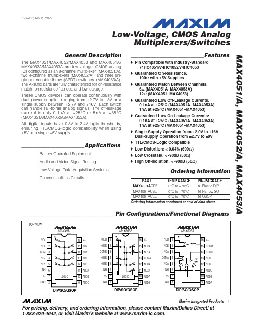
VCOM = ±3V
MAX4051, TA = +25°C
12
MAX4052,
MAX4053 C, E, M
MAX4051ACPE来自0°C to +70°C 16 Plastic DIP
MAX4051ACSE
0°C to +70°C 16 Narrow SO
MAX4051ACEE
0°C to +70°C 16 QSOP
Ordering Information continued at end of data sheet.
For pricing, delivery, and ordering information, please contact Maxim/Dallas Direct! at 1-888-629-4642, or visit Maxim’s website at .
元器件交易网
Storage Temperature Range .............................-65°C to +150°C Lead Temperature (soldering, 10s) .................................+300°C
Note 1: Signals on any terminal exceeding V+ or V- are clamped by internal diodes. Limit forward-diode current to maximum current rating.
Continuous Power Dissipation (TA = +70°C) Plastic DIP (derate 10.53mW/°C above +70°C)............842mW Narrow SO (derate 8.70mW/°C above +70°C)..............696mW QSOP (derate 8.00mW/°C above +70°C) .....................640mW CERDIP (derate 10.00mW/°C above +70°C) ................800mW
MAX490EEPA中文资料
元器件交易网
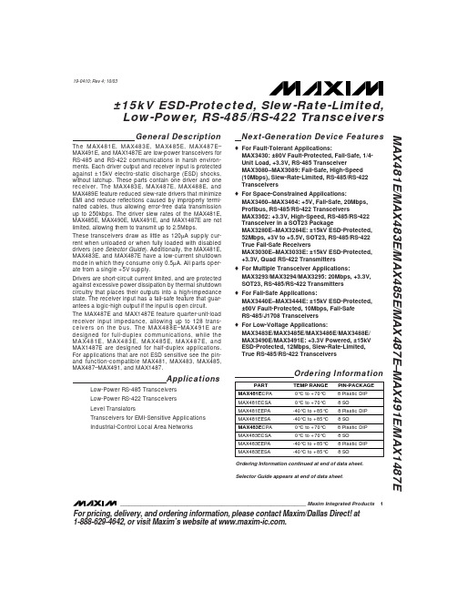
MAX481E/MAX483E/MAX485E/MAX487E–MAX491E/MAX1487E
19-0410; Rev 4; 10/03
±15kV ESD-Protected, Slew-Rate-Limited, Low-Power, RS-485/RS-422 Transceivers
Ordering Information
PART MAX481ECPA MAX481ECSA MAX481EEPA MAX481EESA MAX483ECPA MAX483ECSA MAX483EEPA MAX483EESA
TEMP RANGE 0°C to +70°C 0°C to +70°C -40°C to +85°C -40°C to +85°C 0°C to +70°C 0°C to +70°C -40°C to +85°C -40°C to +85°C
- 1、下载文档前请自行甄别文档内容的完整性,平台不提供额外的编辑、内容补充、找答案等附加服务。
- 2、"仅部分预览"的文档,不可在线预览部分如存在完整性等问题,可反馈申请退款(可完整预览的文档不适用该条件!)。
- 3、如文档侵犯您的权益,请联系客服反馈,我们会尽快为您处理(人工客服工作时间:9:00-18:30)。
General DescriptionThe MAX5230/MAX5231 low-power, dual 12-bit voltage-output digital-to-analog converters (DACs) feature an internal 10ppm/°C precision bandgap voltage reference and precision output amplifiers. The MAX5231 operates on a single 5V supply with an internal 2.5V reference and features a 4.095V full-scale output range. The MAX5230operates on a single 3V supply with an internal 1.25V ref-erence and features a 2.0475V full-scale output range.The MAX5231 consumes only 470µA while the MAX5230consumes only 420µA of supply current. Both devices feature low-power (2µA) software- and hardware-enabled shutdown modes.The MAX5230/MAX5231 feature a 13.5MHz SPI ™-,QSPI ™-, and MI CROWI RE™-compatible 3-wire serial interface. An additional data output (DOUT) allows for daisy-chaining and read back. Each DAC has a double-buffered digital input. The MAX5230/MAX5231 feature two software-selectable shutdown output impedances:1k Ωor 200k Ω. A power-up reset feature sets DAC out-puts at ground or at the midscale DAC code.The MAX5230/MAX5231 are specified over the extended temperature range (-40°C to +85°C) and are available in 16-pin QSOP packages.ApplicationsIndustrial Process Controls Automatic Test Equipment Digital Offset and Gain Adjustment Motion Control µP-Controlled SystemsFeatures♦Internal 10ppm/°C Precision Bandgap Reference2.465V (MAX5231)1.234V (MAX5230)♦Single-Supply Operation5V (MAX5231)3V (MAX5230)♦Low Supply Current470µA (MAX5231)420µA (MAX5230)♦13.5MHz SPI/QSPI/MICROWIRE-Compatible, 3-Wire Serial Interface ♦Pin-Programmable Power-Up Reset State to Zero or Midscale Output Voltage ♦Programmable Shutdown Modes with 1k Ωor 200k ΩInternal Output Loads ♦Recalls Output State Prior to Shutdown or Reset ♦Buffered Output Drives 5k Ω|| 100pF Loads ♦Space-Saving 16-Pin QSOP PackageMAX5230/MAX52313V/5V , 12-Bit, Serial Voltage-Output Dual DACswith Internal Reference________________________________________________________________Maxim Integrated Products 1Ordering Information19-2332; Rev 2; 9/08For pricing delivery, and ordering information please contact Maxim Direct at 1-888-629-4642,or visit Maxim’s website at .Functional Diagram appears at end of data sheet.SPI and QSPI are trademarks of Motorola, Inc.MICROWIRE is a trademark of National Semiconductor, Corp.Pin Configuration+M A X 5230/M A X 52313V/5V , 12-Bit, Serial Voltage-Output Dual DACs with Internal Reference 2_______________________________________________________________________________________ABSOLUTE MAXIMUM RATINGSELECTRICAL CHARACTERISTICS—MAX5231Stresses beyond those listed under “Absolute Maximum Ratings” may cause permanent damage to the device. These are stress ratings only, and functional operation of the device at these or any other conditions beyond those indicated in the operational sections of the specifications is not implied. Exposure to absolute maximum rating conditions for extended periods may affect device reliability.V DD to AGND, DGND...............................................-0.3V to +6V AGND to DGND.....................................................-0.3V to +0.3V Digital Inputs to DGND.............................................-0.3V to +6V Digital Output (DOUT) to DGND...................-0.3V to V DD + 0.3V OUT_ to AGND.............................................-0.3V to V DD + 0.3V OS_ to AGND...................................................-4V to V DD + 0.3VMaximum Current into Any Pin............................................50mA Continuous Power Dissipation (T A = +70°C)16-Pin QSOP (derate 8.3mW/°C above +70°C)...........667mW Operating Temperature Range ...........................-40°C to +85°C Storage Temperature Range.............................-65°C to +150°C Lead Temperature (soldering, 10s).................................+300°CMAX5230/MAX52313V/5V , 12-Bit, Serial Voltage-Output Dual DACswith Internal Reference_______________________________________________________________________________________3ELECTRICAL CHARACTERISTICS—MAX5231 (continued)(V DD = +4.5V to +5.5V, OS_ = AGND = DGND = 0, R L = 5k Ω, C L = 100pF, T A = T MIN to T MAX , unless otherwise noted. Typical values are at T= +25°C.)ELECTRICAL CHARACTERISTICS—MAX5230(V= +2.7V to +3.6V, OS_ = AGND = DGND = 0, R = 5k Ω, C = 100pF, T = T to T , unless otherwise noted. Typical valuesM A X 5230/M A X 52313V/5V , 12-Bit, Serial Voltage-Output Dual DACs with Internal Reference 4_______________________________________________________________________________________ELECTRICAL CHARACTERISTICS—MAX5230 (continued)(V DD = +2.7V to +3.6V, OS_ = AGND = DGND = 0, R L = 5k Ω, C L = 100pF, T A = T MIN to T MAX , unless otherwise noted. Typical values are at T= +25°C.)MAX5230/MAX52313V/5V , 12-Bit, Serial Voltage-Output Dual DACswith Internal ReferenceNote 1:Note 2:Note 3:∆V OUT over the temperature range isdivided by ∆T.Note 4:DC crosstalk is measured as follows: set DAC A to midscale, and DAC B to zero, and measure DAC A output; then changeDAC B to full scale, and measure ∆V OUT for DAC A. Repeat the same measurement with DAC A and DAC B interchanged.DC crosstalk is the maximum ∆V OUT measured.Note 5:Accuracy is better than 1LSB for V OUT_= 10mV to V DD - 180mV. Note 6:Guaranteed by design, not production tested.Note 7:R LOAD = ∞and digital inputs are at either V DD or DGND.TIMING CHARACTERISTICS—MAX5231(V DD = +4.5V to +5.5V, AGND = DGND = 0, T A = T MINto T MAX , unless otherwise noted. Typical values are at T A = +25°C.) ELECTRICAL CHARACTERISTICS—MAX5230 (continued)(V = +2.7V to +3.6V, OS_ = AGND = DGND = 0, R = 5k Ω, C = 100pF, T = T to T , unless otherwise noted. Typical valuesM A X 5230/M A X 52313V/5V , 12-Bit, Serial Voltage-Output Dual DACs with Internal Reference 6_______________________________________________________________________________________TIMING CHARACTERISTICS—MAX5230(V DD = +2.7V to +3.6V, AGND = DGND = 0, T A = T MIN to T MAX , unless otherwise noted. Typical values are at T A = +25°C.)contents.INTEGRAL NONLINEARITYvs. DIGITAL INPUT CODE (MAX5230)M A X 5230/M A X 5231 t o c 01DIGITAL INPUT CODEI N L (L S B )40003500300025002000150010005000-0.10-0.0500.050.100.15-0.15INTEGRAL NONLINEARITYvs. DIGITAL INPUT CODE (MAX5231)M A X 5230/M A X 5231 t o c 02DIGITAL INPUT CODEI N L (L S B )40003500300025002000150010005000-0.10-0.0500.050.100.15-0.15DIFFERENTIAL NONLINEARITY vs. DIGITAL INPUT CODE (MAX5230)M A X 5230/M A X 5231 t o c 03DIGITAL INPUT CODED N L (L S B )40003500300025002000150010005000-0.283-0.0370.0860.208-0.160Typical Operating Characteristics(V DD = +3V (MAX5230), V DD = +5V (MAX5231), R L = 5k Ω, C L = 100pF, OS_ = AGND, both DACs enabled with full-scale output code,T A = +25°C, unless otherwise noted.)MAX5230/MAX52313V/5V , 12-Bit, Serial Voltage-Output Dual DACswith Internal Reference_______________________________________________________________________________________7DIFFERENTIAL NONLINEARITY vs. DIGITAL INPUT CODE (MAX5231)M A X 5230/M A X 5231 t o c 04DIGITAL INPUT CODED N L (L S B )40003500300025002000150010005000-0.10-0.0500.050.100.15-0.15SUPPLY CURRENT vs. TEMPERATURE(MAX5230)M A X 5230/M A X 5231 t o c 05TEMPERATURE (°C)S U P P L Y C U R R E N T (µA )603510-15410420430440450400-4085SUPPLY CURRENT vs. TEMPERATURE(MAX5231)M A X 5230/M A X 5231 t o c 06TEMPERATURE (°C)S U P P L Y C U R R E N T (µA )603510-15410420430440450400-4085SUPPLY CURRENT vs. SUPPLY VOLTAGE(MAX5230)M A X 5230/M A X 5231 t o c 07SUPPLY VOLTAGE (V)S U P P L Y C U R R E N T (µA )3.33.04054104154204254304002.73.6SUPPLY CURRENT vs. SUPPLY VOLTAGE(MAX5231)M A X 5230/M A X 5231 t o c 08SUPPLY VOLTAGE (V)S U P P L Y C U R R E N T (µA )5.255.004.754654704754804854904604.505.50FULL POWER-DOWN SUPPLY CURRENTvs. TEMPERATURE (MAX5230)TEMPERATURE (°C)S U P P L Y C U R R E N T (µA )6035-15100.450.500.550.600.650.700.750.800.40-4085TWO-DACs SHUTDOWN SUPPLY CURRENTvs. TEMPERATURE (MAX5230)TEMPERATURE (°C)S U P P L Y C U R R E N T (µA )603510-15205210215220225230200-4085ONE-DAC SHUTDOWN SUPPLY CURRENTvs. TEMPERATURE (MAX5230)TEMPERATURE (°C)S U P P L Y C U R R E N T (µA )603510-15305310315320325330300-4085FULL POWER-DOWN SUPPLY CURRENTvs. TEMPERATURE (MAX5231)TEMPERATURE (°C)S U P P L Y C U R R E N T (µA )6035-15100.50.60.70.80.91.01.11.20.4-4085Typical Operating Characteristics (continued)(V DD = +3V (MAX5230), V DD = +5V (MAX5231), R L = 5k Ω, C L = 100pF, OS_ = AGND, both DACs enabled with full-scale output code, T A = +25°C, unless otherwise noted.)M A X 5230/M A X 52313V/5V , 12-Bit, Serial Voltage-Output Dual DACs with Internal Reference 8_______________________________________________________________________________________Typical Operating Characteristics (continued)(V DD = +3V (MAX5230), V DD = +5V (MAX5231), R L = 5k Ω, C L = 100pF, OS_ = AGND, both DACs enabled with full-scale output code, T A = +25°C, unless otherwise noted.)TWO-DACs SHUTDOWN SUPPLY CURRENTvs. TEMPERATURE (MAX5231)TEMPERATURE (°C)S U P P L Y C U R R E N T (µA )603510-15230235240245250255225-4085ONE-DAC SHUTDOWN SUPPLY CURRENTvs. TEMPERATURE (MAX5231)TEMPERATURE (°C)S U P P L Y C U R R E N T (µA )603510-15355360365370375380350-4085FULL-SCALE OUTPUT VOLTAGE vs. TEMPERATURE (MAX5230)TEMPERATURE (°C)F U L L -S C A L E O U T P U T V O L T AG E (V )603510-152.04652.04702.04752.04802.0460-4085FULL-SCALE OUTPUT VOLTAGE vs. TEMPERATURE (MAX5231)TEMPERATURE (°C)F U L L -S C A L E O U T P U T V O L T AG E (V )603510-154.09154.09204.09254.09304.09354.09404.0910-4085FULL-SCALE ERROR vs. RESISTIVE LOAD(MAX5230)RESISTIVE LOAD (k Ω)F U L L -S C A L E E R R O R (L S B )6.55.54.53.50.050.100.150.200.250.300.3502.57.5FULL-SCALE ERROR vs. RESISTIVE LOAD(MAX5231)RESISTIVE LOAD (k Ω)F U L L -S C A L E E R R O R (L S B )6.55.54.53.50.050.100.150.200.252.57.5DYNAMIC RESPONSE RISE TIME(MAX5230)MAX5230/MAX5231 toc192µs/divV OUT 500mV/divV CS 2V/div2.048V3V 010mVDYNAMIC RESPONSE RISE TIME(MAX5231)MAX5230/MAX5231 toc202µs/divV OUT 1V/divV CS 5V/div4.096V5V 010mVDYNAMIC RESPONSE FALL TIME(MAX5230)MAX5230/MAX5231 toc212µs/divV OUT 500mV/divV CS 2V/div2.048V3V 010mVMAX5230/MAX52313V/5V , 12-Bit, Serial Voltage-Output Dual DACswith Internal Reference_______________________________________________________________________________________9DYNAMIC RESPONSE FALL TIME(MAX5231)MAX5230/MAX5231 toc222µs/divVOUT 1V/divV CS 5V/div4.096V5V 010mVANALOG CROSSTALK(MAX5230)MAX5230/MAX5231 toc23400µs/div OUTB 5mV/div AC-COUPLED OUTA 2V/div ANALOG CROSSTALK(MAX5231)MAX5230/MAX5231 toc24400µs/divOUTB 5mV/div AC-COUPLEDOUTA 5V/divDIGITAL FEEDTHROUGH(MAX5230)MAX5230/MAX5231 toc2510µs/div OUTA 1mV/div AC-COUPLED SCLK 2V/div DIGITAL FEEDTHROUGH(MAX5231)MAX5230/MAX5231 toc2610µs/div OUTA 1mV/div AC-COUPLEDSCLK 5V/div MAJOR-CARRY TRANSITION(MAX5230)MAX5230/MAX5231 toc272µs/divOUTA 100mV/div AC-COUPLEDCS 5V/divMAJOR-CARRY TRANSITION(MAX5231)MAX5230/MAX5231 toc282µs/div OUTA 100mV/div AC-COUPLEDCS 5V/divREFERENCE VOLTAGE vs. TEMPERATURE (MAX5230)TEMPERATURE (°C)R E F E R E N C E V O L T A G E (V )603510-151.23351.23401.23451.23501.2330-4085REFERENCE VOLTAGEvs. TEMPERATURE (MAX5231)TEMPERATURE (°C)R E F E R E N C E V O L T A G E (V )603510-152.46152.46202.46252.46302.4610-4085Typical Operating Characteristics (continued)(V DD = +3V (MAX5230), V DD = +5V (MAX5231), R L = 5k Ω, C L = 100pF, OS_ = AGND, both DACs enabled with full-scale output code, T A = +25°C, unless otherwise noted.)M A X 5230/M A X 52313V/5V , 12-Bit, Serial Voltage-Output Dual DACs with Internal Reference 10______________________________________________________________________________________Detailed DescriptionThe MAX5230/MAX5231 12-bit, voltage-output DACs are easily configured with a 3-wire SPI -, QSPI -,MI CROWI RE-compatible serial interface. The devices include a 16-bit data-in/data-out shift register and have an input consisting of an input register and a DAC reg-ister. I n addition, these devices employ precision trimmed internal resistors to produce a gain of 1.6384V/V, maximizing the output voltage swing, and a programmable-shutdown output impedance of 1k Ωor 200k ΩThe full-scale output voltage is 4.095V for the MAX5231 and 2.0475V for the MAX5230. These devices produce a weighted output voltage proportion-al to the digital input code with an inverted rail-to-rail ladder network (Figure 3).Internal ReferenceThe MAX5230/MAX5231 use an on-board precision bandgap reference to generate an output voltage of 1.234V (MAX5230) or 2.465V (MAX5231). With a low temperature coefficient of only 10ppm/°C, REF can source up to 100µA and is stable for capacitive loads less than 35pF.Output AmplifiersThe output amplifiers have internal resistors that pro-vide for a gain of 1.6384V/V when OS_ is connected to AGND. The output amplifiers have a typical slew rate of0.6V/µs and settle to 1/2LSB within 10µs with a load of 5k Ωin parallel with 100pF. Use the serial interface to set the shutdown output impedance of the amplifiers to 1k Ωor 200k Ω.OS_ can be used to produce an offset voltage at the output. For instance, to achieve a 1V offset, apply -1V to OS_ to produce an output range from 1V to (1V +V FS /V REF ). Note that the DAC’s output range is still lim-ited by the maximum output voltage specification.MAX5230/MAX52313V/5V , 12-Bit, Serial Voltage-Output Dual DACswith Internal Reference______________________________________________________________________________________11Figure 3. Simplified DAC Circuit DiagramM A X 5230/M A X 5231The 3-wire serial interface (SPI , QSPI , MI CROWI RE compatible) used in the MAX5230/MAX5231 allows for complete control of DAC operations (Figures 4 and 5).Figures 1 and 2 show the timing for the serial interface.The serial word consists of 3 control bits followed by 12data bits (MSB first) and 1 sub-bit as described in Tables 1, 2, and 3. When the 3 control bits are all zero or all 1, D11–D8 are used as additional control bits,allowing for greater DAC functionality.The digital inputs allow any of the following: loading the input register(s) without updating the DAC register(s),updating the DAC register(s) from the input register(s),or updating the input and DAC register(s) simultane-ously. The control bits and D11–D8 allow the DACs to operate independently.Send the 16-bit data as one 16-bit word (QSPI) or two 8-bit packets (SPI , MI CROWI RE), with CS low during this period. The control bits and D11–D8 determine which registers update and the state of the registers when exiting shutdown. The 3-bit control and D11–D8determine the following:•Registers to be updated•Selection of the power-down and shutdown modes The general timing diagram of Figure 1 illustrates data acquisition. Driving CS low enables the device to receive data. Otherwise the interface control circuitry is disabled. With CS low, data at DIN is clocked into the register on the rising edge of SCLK. As CS goes high,data is latched into the input and/or DAC registers,depending on the control bits and D11–D8. The maxi-mum clock frequency guaranteed for proper operation is 13.5MHz. Figure 2 depicts a more detailed timing diagram of the serial interface.3V/5V , 12-Bit, Serial Voltage-Output Dual DACs with Internal Reference 12______________________________________________________________________________________Power-Down and Shutdown ModesAs described in Tables 2 and 3, several serial interface commands put one or both of the DACs into shutdown mode. Shutdown modes are completely independent for each DAC. I n shutdown, the amplifier output be-comes high impedance, and OUT_ terminates to OS_through the 200k Ω(typ) gain resistors. Optionally (see Tables 2 and 3), OUT_ can have an additional termina-tion of 1k Ωto AGND.Full power-down mode shuts down the main bias gene-rator, reference, and both DACs. The shutdown impe-dance of the DAC outputs can still be controlled independently, as described in Tables 2 and 3.A serial interface command exits shutdown mode and updates a DAC register. Each DAC can exit shutdown at the same time or independently (see Tables 2 and 3). For example, if both DACs are shut down, updating the DAC A register causes DAC A to power up, while DAC B remains shut down. I n full power-down mode,powering up either DAC also powers up the main bias generator and reference. To change from full power-down to both DACs shutdown requires the waking of at least one DAC between states.When powering up the MAX5230/MAX5231 (powering V DD ), allow 400µs (max) for the output to stabilize. When exiting full power-down mode, also allow 400µs (max) for the output to stabilize. When exiting DAC shutdown mode, allow 160µs (max) for the output to stabilize.Reset Value (RSTV) andClear (CLR ) InputsDriving CLR low asynchronously forces both DAC out-puts and all the internal registers (input registers and DAC registers) for both DACs to either zero or midscale,depending on the level at RSTV. RSTV = DGND sets the zero value, and RSTV, = V DD sets the midscale value.The internal power-on reset circuit sets the DAC out-puts and internal registers to either zero or midscale when power is first applied to the device, depending on the level at RSTV as described in the preceding para-graph. The DAC outputs are enabled after power is first applied. I n order to obtain the midscale value on power-up (RSTV = V DD ), the voltage on RSTV must rise simultaneously with the V DD supply.Load DAC Input (LDAC )Asserting LDAC asynchronously loads the DAC registers from their corresponding input registers (DACs that are shut down remain shut down). The LDAC input is totally asynchronous and does not require any activity on CS ,SCLK, or DIN in order to take effect. If LDAC is asserted coincident with a rising edge of CS,which executes a serial command modifying the value of either DAC input register, then LDAC must remain asserted for at least 30ns following the CS rising edge. This requirement applies only for serial commands that modify the value of the DAC input registers.Power-Down Lockout Input (PDL )Driving PDL low disables shutdown of either DAC. When PDL is low, serial commands to shut down either DAC are ignored. When either DAC is in shutdown mode, a high-to-low transition on PDL brings the DACs and the refer-ence out of shutdown with DAC outputs set to the state prior to shutdown.MAX5230/MAX52313V/5V , 12-Bit, Serial Voltage-Output Dual DACswith Internal Reference13Figure 4. SPI/QSPI Interface ConnectionsFigure 5. Connections for MICROWIREM A X 5230/M A X 5231Applications InformationDefinitionsIntegral Nonlinearity (INL)Integral nonlinearity (Figure 6a) is the deviation of the val-ues on an actual transfer function from a straight line.This straight line can be either a best-straight-line fit (closest approximation to the actual transfer curve) or a line drawn between the endpoints of the transfer func-tion, once offset and gain errors have been nullified. For a DAC, the deviations are measured at every single step.Differential Nonlinearity (DNL)Differential nonlinearity (Figure 6b) is the difference between an actual step height and the ideal value of 1LSB. If the magnitude of the DNL is less than 1LSB, the DAC guarantees no missing codes and is monotonic.Offset ErrorThe offset error (Figure 6c) is the difference between the ideal and the actual offset point. For a DAC, the off-set point is the step value when the digital input is zero.This error affects all codes by the same amount and can usually be compensated for by trimming.Gain ErrorGain error (Figure 6d) is the difference between the ideal and the actual full-scale output voltage on the transfer curve, after nullifying the offset error. This error alters the slope of the transfer function and corre-sponds to the same percentage error in each step.Settling TimeThe settling time is the amount of time required from the start of a transition, until the DAC output settles to its new output value within the converter’s specified accuracy.3V/5V , 12-Bit, Serial Voltage-Output Dual DACs with Internal Reference 14Digital feedthrough is noise generated on the DAC’s output when any digital input transitions. Proper board layout and grounding significantly reduce this noise,but there is always some feedthrough caused by the DAC itself.Unipolar OutputFigure 7 shows the MAX5230/MAX5231 configured for unipolar, rail-to-rail operation. The MAX5231 produces a 0 to 4.095V output, while the MAX5230 produces 0 to 2.0475V output. Table 4 lists the unipolar output codes.Digital Calibration and Threshold SelectionFigure 8 shows the MAX5230/MAX5231 in a digital cali-bration application. With a bright light value applied to the photodiode (on), the DAC is digitally ramped until it trips the comparator. The microprocessor (µP) stores this “high” calibration value. Repeat the process with a dim light (off) to obtain the dark current calibration. The µP then programs the DAC to set an output voltage at the midpoint of the two calibrated values. Applications include tachometers, motion sensing, automatic read-ers, and liquid clarity analysis.Sharing a Common DIN LineSeveral MAX5230/MAX5231s may share one common DIN signal line (Figure 9). In this configuration, the data bus is common to all devices; data is not shifted through a daisy-chain. The SCLK and DIN lines are shared by all devices, but each IC needs its own dedicated CS line.Daisy-Chaining DevicesAny number of MAX5230/MAX5231s can be daisy-chained by connecting the serial data output (DOUT) of one device to the digital input (DI N) of the following device in the chain (Figure 10).MAX5230/MAX52313V/5V , 12-Bit, Serial Voltage-Output Dual DACswith Internal Reference______________________________________________________________________________________15M A X 5230/M A X 5231Power-Supply and BypassingConsiderationsOn power-up, the input and DAC registers are cleared to either zero (RSTV = DGND) or midscale (RSTV =V DD ). Bypass V DD with a 4.7µF capacitor in parallel with a 0.1µF capacitor to AGND, and bypass V DD with a 0.1µF capacitor to DGND. Minimize lead lengths to reduce lead inductance.Grounding and Layout ConsiderationsDigital and AC transient signals on AGND or DGND can create noise at the output. Connect AGND and DGND to the highest quality ground available. Use propergrounding techniques, such as a multilayer board with a low-inductance ground plane or star connect all ground return paths back to the MAX5230/MAX5231 AGND.Carefully lay out the traces between channels to reduce AC cross-coupling and crosstalk. Wire-wrapped boards and sockets are not recommended. I f noise becomes an issue, shielding may be required.Chip InformationTRANSISTOR COUNT: 4745PROCESS: BiCMOS3V/5V , 12-Bit, Serial Voltage-Output Dual DACs with Internal Reference 16______________________________________________________________________________________Figure 9. Multiple MAX5230/MAX5231s Sharing a Common DIN LineMAX5230/MAX52313V/5V , 12-Bit, Serial Voltage-Output Dual DACswith Internal Reference______________________________________________________________________________________17Functional DiagramPackage InformationFor the latest package outline information and land patterns, go to /packages .M A X 5230/M A X 52313V/5V , 12-Bit, Serial Voltage-Output Dual DACs with Internal Reference Maxim cannot assume responsibility for use of any circuitry other than circuitry entirely embodied in a Maxim product. No circuit patent licenses are implied. Maxim reserves the right to change the circuitry and specifications without notice at any time.18____________________Maxim Integrated Products, 120 San Gabriel Drive, Sunnyvale, CA 94086 408-737-7600©2008 Maxim Integrated Productsis a registered trademark of Maxim Integrated Products, Inc.。