5082-A111-EL000中文资料
UL 508认证标准(中文版)

UL508P83-100设备性能42综述42.1工业控制设备的性能应该通过按照43-61B 节中所描述的试验项目对典型样品或商业贸易中的样品进行试验来验证并要求那些测试按照表42.1所示的操作顺序进行42.2那些导致某一测试项目终止的温度或电流敏感设备或系统应该进行附加的评估测试来确定他们适用于其应用场合42.3除非特别说明测试应采用表42.2中所指定的实际使用电压的额定频率42.4除非特别说明测试应在10-4050-104℉的任意环境温度下进行环境温度的测量应采用在设备的附近安装温度计或热电偶的方法测量42.5对于有不完全封闭或局部外壳的工业控制设备将在本标准中被作为一个开放式无外壳设备来考虑其性能要求表42.1测试顺序样品数量 注1 2 标准参考条款试验项目 顺序 顺序 43 44 45 46 49温升测试过电压和欠电压测试 过负载测试 耐久性测试 介质耐压测试1 2 31 2 3注所有或任一个试验顺序的分组取决于单一样品是否适用任何一个试验顺序没有必要作为进行其他试验项目的首要条件表42.2测试电压值设备的额定电压试验项目110-120 220-240 254-277 380-415 440-480 560-600标准条款编号温升测试 120 240 277 415 480 600 43 过电压试验 AC / DC 132 264 305 457 528 660 44 欠电压试验AC 102 204 235 353 408 510 44 欠电压试验DC96 192 222 332 384 480 44过负载 120 240 277 415 480 600 45 耐久性 120 240 277 415 480 600 46a如果设备的额定值不落在表中的任何电压值范围内除了过压测试和欠压测试见43.8外都以设备的额定电压值作为他的测试值42.6敞开式设备应安装在一个被认为是预期典型使用的罩壳内最大罩壳尺寸可以通过以下任一方法来确定a设备长宽高三尺寸的150%b尺寸符合表6.8所列的导线弯曲空间c预期的罩壳如一标准出路盒子或d预期的罩壳假如标注在设备或卡片上的尺寸可以比42.6a-42.6c所确定的尺寸大例外如36.7a所指定继电器的不必要这样测试 [注36.7a额定功率为1马力输出功率746瓦或相当的FLA或者更小的720伏安断开控制器功率或更小或电压为51-150伏时电流不大于15安培电压为151-300伏时电流不大于10安培或电压为301-600伏时电流不大于5安培]42.7为了进行测试将有两个或更多开-关位置的换向控制器切换开关仪表开关双回路或三回路装置或其他类型的装置进行连接以便使正常使用中会出现的相反极性施加于断开触点或零件之间参见64.1 [注64.1导线接线端应明确标识导线连接的适当的电源负载控制回路等类似的或者一配线表代码以确保能够安全连接设备例外1至于一双接线端开关装置导线连接是非常明白的接线端不必标识例外2在安装配线表说明书后如数目方面可以独立的提供具有多样回路安装的配线表或者在一封袋上提供名牌或类似永久的显著的附件例外3对于一开放式设备配线表可以与设备分开提供]例外明确标识有极性的设备应按标识所指的极性进行连接42.8在测试期间设备应是处于约定的正常连接和安装状态以体现正常使用状态除了体现终端扭矩测试59节所有导线终端模块或导线连接器接线端子应按照产品注明的扭矩力值紧固43温度测试43.1在43.2-43.27描述的条件下进行测试工业控制设备应满足以下要求a不达到对设备上所采用的材料构成着火危险或不利影响的高温b不能超过设备中任何一个零部件的极限温度以及c在特定测试点不能超过表43.1描述的温升值43.2在表43.1所列的所有温升值适用于约定最高允许环境温度为40的设备43.3 43.3和43.5合并和重新修订43.4 删除43.5 43.3和43.5合并和重新修订43.6 假如工业控制设备约定最高允许环境温度高于40则在这更高环境温度下允许的温升按照如下计算公式计算TR = TT- [TM- 40]其中T R 允许的温升值T T 表43.1所允许的最大温度升高TM设备上所标识的更高环境温度见62.1.1 [注设备应该服役在规定的额定的40的温度条件下或高于或低于40并且以5的整数倍为间隔如45505560]43.7 假如工业控制设备约定最高允许环境温度低于40则在这较低环境温度下允许的温升按照如下计算公式计算T R = T T + 40 - T M其中T R允许的温升值T T 表43.1所允许的最大温度升高T M设备上所标识的较低环境温度见62.1.143.8测试时线圈电压应按照表42.2所列然而当制造厂商提供了在表42.2所列每一指定电压范围内如110115或120伏特的不同额定电压变压器或电磁铁线圈以及如果线圈是采用每一额定范围内的最大值激励则应该对每一电压范围内的典型线圈规格按照44.1条明确的百分比确定试验电压进行测试如果线圈没有提供在每一范围内的最大电压等级测试应控制在表42.2所列的所有线圈测试电压43.9为了确定工业控制设备是否达到温度测试的要求应该按照以下条件进行操作a 在正常条件下b 连续通以额定电流见43.1-43.13条c 给线圈施加如表42.2或43.8条所规定的电压例外除了线圈额定电压以外的低压电源可以代替规定的电压值用于零部件的温度测试 d 约定的安装方式见43.14和43.16条e 在43.17条所规定的环境温度下f需要达到温度稳定见43.25条在测试的结果方面每一种材料或部件的温升不能超过在43.143.6和43.7条中所列的最大温升值一种材料或部件的温升是其稳定时温度与测试环境温度之间的差值在测试过程中保护装置或线路不应动作对于按照43.17条a测试的具有温控装置或其他热保护装置的设备这些温度装置的动作温度应该予以测量并修正环境温度的差值通过将修正后的温度值与保护装置动作温度比较以确定是否该设备发生温度保护并将其作为测试的结果43.10由于某一部件的发热可能会影响到其他部件的发热所以应该在所有部件同时工作时进行温度的测量43.11设备额定马力所对应的额定电流如表45.245.362.2或62.3所示表43.1最大温升 材料和部件℉1 闸刀开关的刀片和接触口 30 542 当用虚拟保险丝模拟一个用于保护支路回路的保险丝测试的保险丝夹子 30 54 3当用为了保护支路回路的测试的保险丝夹子o85 1534 橡胶或热塑形绝缘材料 aa5接线端配线区域c,k,i设备标识为60或60/75的应用导线设备标识为75的应用导线5065901176总线和接线板或接线棒d 7 触点纯以及复合银银合金以及镀银其他所有材料e65e1178 绝缘系统105级绝缘系统 f热电偶法电阻法105A级绝缘系统用于单层series非绝缘或上漆裸露线圈热电偶法120E级绝缘系统f r热电偶法电阻法130B级绝缘系统f r热电偶法电阻法155F级绝缘系统f r热电偶法电阻法180H级绝缘系统f r热电偶法电阻法200N级绝缘系统f r热电偶法电阻法220R级绝缘系统f r热电偶法电阻法658590759585105951151151351351551551751171261621351711531891712072072432432792793159 绝缘材料 b p p10 在流动空气环境下距离设备外壳1英尺25.4mm处 175175 11 固定电阻和可变电阻的包裹材料内含阻性元器件的墙面安装型调光器 300 54012 已经内置阻性导体并用于安装在配电盘或不可燃的框架内的变阻调光350 630器的包裹材料67513 裸露的电阻材料热电偶法 375g14 电容 g15 功率切换半导体器件 mmn16 印刷线路板 nq17 1-16项中没有规定的材料和部件 qa 对于绝缘导体最大温升不能超过规定的导线所讨论的减去一个假定的室内温度40的最大工作温度b对于已经调查过的特殊的额定温度的复合最大温升不能超过额定温度减去假定的环境温度40c配线接线端或接线片的最有可能被接触点的温度的测量通过绝缘导体作为实际服务安装d界限不能用于连接热源如电阻器和一过载继电器的电流元件e通过相临部分材料的温度界限的温度极点见43.18不能有接触装配结构变化部件的松开破裂或材料的剥落簧片韧度降低部件的退火或其他明显的损伤f见43.19-43.25g对于一电容器最大温升是电容标识限定温度减去40h删除i当升高值是50或低于打算用一个铝才连接器或铝导线连接器应按AL7CU或AL9CU标识当接线端温升在50-65之间时连接器的标识应为AL9CUj删除k见63.3l极限值仅仅是用于线路板bus bars和用于工业控制装置功率分分布的接线板极限值不应用于位于工业控制装置短片的铜板和用于固定接触单元或工厂或配线区终端这种结构类型的最大温升取决于所用材料的的温度限定值材料的临近部分或者在铜材表面最低的温升100他们不能有装配结构的恶化部件的松散开裂或材料的剥落簧片韧度的降低部件的退火或其他明显的损伤m在这种条件下的最大温升是这种最大条件下温度应用于被半导体制造商推荐的功率消耗减去40n印刷线路板的最大温升是线路板的工作温度减去40o见63.23p见表15.2和37.1q任何组件的最大温升不能超过组件的极限温度减去40r绝缘系统应该符合UL1446绝缘材料系统标准综述的要求43.12对于电流特性表中具有最小和最大满负载电机电流的设备温度测试应采用表中所列的最大满负载电流进行即使这个电流超过了设备的最大额定电流对于电流特性表中只是稳态tripping电流的设备测试电流应采用所规定的最大稳态电流的87%43.13对于直接安装在接触器或启动器上的一个辅助开关测试电流应符合与额定切换电流相一致的最大分断电流43.14工业控制设备的测试应采用1.2m长的导线来连接每一接线端比如当导体是连接在两个接线端子之间则需要用2.4m长的导线导线的最小允许规格应至少能够承受以下负载的125%a与表45.2或45.3相一致的最大满载电机电流适当的至少对于其他负载的100%b对于如表43.1所列具有最高额定电流特性应用了可更换电流元件的过载装置的设备采用其最大满负载电机电流c对于采用过载继电器和应用了不可更换电流元件过载继电器的设备采用其最大满负载电机电流导线的大小应根据设备上导线温度等级标识并与表43.2相一致绝缘类型没有特别规定温度测试可以采用非黑色绝缘层的导线进行连接但是在仲裁测量时应采用黑色绝缘层的导线进行连接如果接线端不能达到43.12条所规定的导线尺寸如具有过载继电器的设备或者如果设备按照25.5.4条有标识限制导线的尺寸则应使用设备所允许的最大尺寸的导线例外当规定额电流在450安培或以上的工业控制设备只能采用线排时应使用厚度为6.4mm铜排其宽度按表43.3规定并且至少需要4英尺 1.2m长温度测试可以采用非黑色绝缘层的铜排进行连接但是在仲裁测量时应采用黑色绝缘层的铜排进行连接除非在个别终端设备有特殊要求铜排间的间隔距离应6.4mm不应有意加大间隔距离表43.2绝缘导体的容量导线尺寸 60 75AWG mm2铜铝铜铝24 0.2 2 - - -22 0.3 3 - - -20 0.5 5 - - -18 0.8 7 - - -16 1.3 10 - - -14 2.1 15 - 15 -12 3.3 20 15 20 1510 5.3 30 25 30 258 8.4 40 30 50 406 13.3 55 40 65 504 21.2 70 55 85 653 26.7 85 65 100 752 33.6 95 75 115 901 42.4 110 85 130 1001/0 53.5 150 1202/0 67.4 175 135 3/0 85.0 200 155 4/0 107.2230 180kcmil 250 127 255 205 300 152 285 230 350 177 310 250 400 203 335 270 500 253 380 310 600 304 420 340 700 355 460 375 750 380 475 385 800 405 490 395 900 456 520 425 1000 506 545 445 1250 633 590 485 1500 760 625 520 1750 887 650 545 2000 1013665 560注1对于接线端具有相同尺寸1/0AWG 或更大多重导体容量等于表43.2中对应导体的值乘以接线端所能容纳导体的数量2那些容量值仅仅适用于在导管安装区至多三根导线如果四根或更多导线除了一中性的带不稳定电流的导线外其他的将安装在一导管内有可能发生因为导管中心数规定设备的输出数导体的量必然是一多相体系或其他原因每一导体的容量是如果包括4-6根导体则是他们值的80%如果是7-24根则是70%25-42根则是60%如果大于或等于43根则是50%表43.3铜线路板的宽度线路板的宽度产品额定值安培线路板每一接线端英尺 毫米 450-600 1 2 51 601-1000 1 3 76 1001-1200 1 4 102 1201-1600 2 3 76 1601-2000 241022001-2500 2 5 1274 2-1/2 642501-3000 3 5 1274 4 10243.15当要求仲裁测量的环境温度时应将几个温度计或热电偶放在设备周围的不同点上温度计或热电偶应放在冷却介质能够进入的地方并防止气流和异常的热辐射环境温度意味着读取的温度值在同样的距离时间决定性于测试最后环境持续环境温度代表着在连续测试的最后测试阶段相同时间间隔内的温度读数43.16封闭式的工业控制设备的测量是在制造商提供的封闭条件下开放型的工业控制设备的测量应在封闭式环境如42.6所描述例外当标识大气环境温度等级时开放型工业控制设备没有要求在封闭式条件下测试43.17温度测试应与设备所放置的环境有关a环境条件与42.4一致b一个无空气循环的测试空间用环境温度的空间测试适合环境等级43.18可接受性绝缘材料不同于其他在表43.1所描述的是由与性能相关如可燃性抗电弧性等之类决定的基于工作温度相当于测量温度的升高加上40或其他标识环境温度等级43.19在表43.1中所规定的热电偶方法的温度测量由用电位计工具类型测量的温度和应用于易受热影响的热电偶组成热电偶是由不大于0.21mm2不小于0.05mm2的导线制成的热电偶和相关的工具应是精确和校准的与实验室规定一致的热电偶导线是符合特殊热电偶在温度测量热电偶ANSI/ISA MC96.1-1982方面的要求的43.20热电偶的连接和靠近热电偶头导线应可靠地安装控制在温度得到测量的材料表面良好的热接触在大多数情况下适当的热接触将由可靠轻拍或接合在热电偶的适当位置产生但是如果材料表面是棘手的铜焊的或焊接热电偶与金属是必要的43.21电阻法测温度具体参见表40.1计算线圈温升用方程t=(r2/r1)(k+t1)-(k+t2)t是线圈温升单位为Cr2是测试最后的线圈电阻单位欧姆r1是开始测试时的线圈电阻单位欧姆t1在开始测试时的室内温度单位为Ct2在测试最后的室内温度单位为Ck对于铜是234.5对于电传导等级EC铝是225.0对于其它传导体具体数值另外确定43.22因为在测量r2前去激励一般是必要的r2在试验停止后准确的数值可能由在短的时间间隔电阻测量决定的在试验停止后马上测量电阻值的曲线变化和时间可以区分和推断以确定试验刚结束时r2的值43.23测量线圈温度的首选方法是电阻法但温度的测量不论是用热电偶还是用电阻法都已被广泛接受除了热电偶法不被使用在使用辅助绝缘任何点以外43.24参考43.23当热电偶用于测量线圈的温度时至少应使用两热电偶计热电偶应放在线圈导线加绝缘在测试过程中定位方向的上表面另外附加的热电偶放在受到另一热源影响的表面比如其他变压器或热电阻器43.25当三次连续读数时间间隔在过去的10%持续测试但不少于10分钟间隔所显示的温升没变化温升是被作为恒量的43.26红外线热分析可用于确定温度测试时热电偶所放位置的最大温度43.27机械接触装置接触部分的清洁不能用研磨剂也不能用腐蚀的方法或在温度测试前采用几次的循环负载44过压和欠压测试44.1一个含有一个或多个电磁开关部件的装配单元应能经受住110%的额定电压而不损害工作绕组并且对于直流应能在其额定电压的80%下正常工作交流应能在其额定电压的85%下正常工作44.2如果设备如具有控制回路变压器的组合电机控制装置进行欠压测试时施加于变压器原边的电压应为变压器原边额定电压的90%44.3首先应在测试温度的条件下激励磁路直到线圈温度达到稳定为止接下来控制回路电压将降低到44.1条中所规定的欠压测试的电压然后开断几次控制回路以确定最后衔铁是否能够完全闭合44.4控制回路的电压升高到45.1条中所规定的过载电压测试值直到用热电偶法测得温度稳定为止然后电压迅速降低到温度测试的电压值马上让控制回路开断几次以确定最后衔铁是否能够完全闭合44.5对于用于周期性负载的电磁铁应进行测试以便确定是否符合44.1-44.4条的规定如果当触点闭合时电阻是接入到电磁铁电路中则当线圈在温度测试条件进行激活时该电阻也应包括在电路中45过载测试45.1在本节所规定的过载测试中设备应没有电气性能或机械性能的下降触点上没有过度的烧损或凹陷触点不发生粘接45.13条中所规定的保险丝不应断开45.2工业控制设备的导线和负载的接线端间隙应具有符合量符合UL840标准第5节电气设备的绝缘间隙和爬电距离中过压控制要求的B级间隙在额定工作下带载和空载时应监测导线和负载的接线端的过电压产生的电压不能高于UL840表5.1条中所规定的最小浪涌耐受电压在过载测试过程中应该通过示波器分析的手段来实现监测45.3用于测试的导线容量最少应为表45.2或45.3所规定的满负载电机电流的125%适当的或最少是其它负载的100%表45.1过载测试回路设备约定应用场合电流安培功率因素全线交流电机启动单相6倍设备满负载电流 0.40-0.50 全线交流电机启动双相和三相测试电流见表45.4 0.40-0.50 全线直流电机启动 10倍设备满负载电流 dc a直流常规回路 1.5倍设备额定值 dc a交流常规回路 1.5倍设备额定值 0.75-0.80 直流阻性回路 1.5倍设备额定值 dc a交流阻性回路 1.5倍设备额定值 1.0 交流阻性空气加热 1.5倍设备额定值 1.0 直流阻性空气加热 1.5倍设备额定值 dc a交流白炽灯钨 1.5倍设备额定值 0.75-0.80 直流白炽灯钨 1.5倍设备额定值 dc 交流电放电管镇流器 3.0倍设备额定值 0.40-0.50 升降机控制交流hp b升降机控制直流hp b容性开关kVar 1.5倍设备额定值 c NOTE-测试循环应按45.12所述A负载是个无电感的阻性负载B升降机控制器要求无过载条件C负载是由商用电容器组成表45.2满负载电机运转电流安培数对应的各种各样a-c马力等级110-120V 200 V 208 V 220-240V b380-415 V 440-480 V 550-600 V马力单相三相单相三相单相三相单相三相单相三相单相三相单相三相1/10 3.0 -- -- -- -- -- 1.5 -- 1.0 -- -- -- -- --1/8 3.8 -- -- -- -- -- 1.9 -- 1.2 -- -- -- -- --1/6 4.4 -- 2.5 -- 2.4 -- 2.2 -- 1.4 -- -- -- -- --1/4 5.8 -- 3.3 -- 3.2 -- 2.9 -- 1.8 -- -- -- -- --1/3 7.2 -- 4.1 -- 4.0 -- 3.6 -- 2.3 -- -- -- -- --1/2 9.8 4.4 5.6 2.5 5.4 2.4 4.9 2.2 3.2 1.3 2.5 1.1 2.0 0.93/4 13.8 6.4 7.9 3.7 7.6 3.5 6.9 3.2 4.5 1.8 3.5 1.6 2.8 1.31 16.0 8.4 9.2 4.8 8.8 4.6 8.0 4.2 5.1 2.3 4.0 2.1 3.2 1.720.0 12.0 11.5 6.9 11.0 6.6 10.0 6.0 6.4 3.3 5.0 3.0 4.0 2.41-1/22 24.0 13.6 13.8 7.8 13.2 7.5 12.0 6.8 7.7 4.3 6.0 3.4 4.8 2.73 34.0 19.2 19.6 11.0 18.7 10.6 17.0 9.6 10.9 6.1 8.5 4.8 6.8 3.95 56.0 30.4 32.2 17.5 30.8 16.7 28.0 15.2 17.9 9.7 14.0 7.6 11.2 6.17-1/80.0 44.0 46.0 25.3 44.0 24.2 40.0 22.0 27.0 14.0 21.0 11.0 16.0 9.0210 100 56.0 57.5 32.2 55.0 30.8 50.0 28.0 33.0 18.0 26.0 14.0 20.0 11.015 135 84.0 -- 48.3 -- 46.2 68.0 42.0 44.0 27.0 34.0 21.0 27.0 17.020 - 108 -- 62.1 -- 59.4 88.0 54.0 56.0 34.0 44.0 27.0 35.0 22.025 - 136 -- 78.2 -- 74.8 110 68.0 70.0 44.0 55.0 34.0 44.0 27.030 - 160 -- 92 -- 88 136 80.0 87.0 51.0 68.0 40.0 54.0 32.040 - 208 -- 120 -- 114 176 104 112 66.0 88.0 52.0 70.0 41.050 - 260 -- 150 -- 143 216 130 139 83.0 108 65.0 86.0 52.0-- 62.060 - -- -- 177 -- 169 -- 154 -- 103 -- 77.0-- 77.075 - -- -- 221 -- 211 -- 192 -- 128 -- 96.0100 - -- -- 285 -- 273 -- 248 -- 165 -- 124 -- 99.0 125 - -- -- 359 -- 343 -- 312 -- 208 -- 156 -- 125150 - -- -- 414 -- 396 -- 360 -- 240 -- 180 -- 144200 - -- -- 552 -- 528 -- 480 -- 320 -- 240 -- 192250 - -- -- -- -- -- -- 604 -- 403 -- 302 -- 242 300 - -- -- -- -- -- -- 722 -- 482 -- 361 -- 289 350 - -- -- -- -- -- -- 828 -- 560 -- 414 -- 336 400 - -- -- -- -- -- -- 954 -- 636 -- 477 -- 382-- -- -- 515 -- 412 450 - -- -- -- -- -- -- 1030-- 786 -- 590 -- 472 500 - -- -- -- -- -- -- 1180A删除B为了得到电机满负载电流265和277伏220-240额定电压相应减少13%和17%表45.3满负载电机运转电流安培数对应的各种各样d-c马力等级马力90V 110-120V 180V 220-240V 500V 550-600V 1/10 -- 2.0 -- 1.0 -- -- 1/8 -- 2.2 -- 1.1 -- -- 1/6 -- 2.4 -- 1.2 -- -- 1/4a 4.0 3.1 2.0 1.6 -- -- 1/3 5.2 4.1 2.6 2.0 -- -- 1/2 6.8 5.4 3.4 2.7 -- -- 3/4 9.6 7.6 4.8 3.8 -- 1.61 12.2 9.5 6.1 4.7 -- 2.01-1/2-- 13.2 8.3 6.6 -- 2.710.8 8.5 -- 3.62 -- 17.03 -- 25.016.0 12.2 -- 5.227.0 20.0 -- 8.35 -- 40.07-1/2 -- 58.0 -- 29.0 -- 12.2 10 -- 76.0 -- 38.0 -- 16.0 15 -- 110.0 -- 55.0 27.0 24.0 20 -- 148.0 -- 72.0 34.0 31.0 25 -- 184.0 -- 89.0 43.0 38.0 30 -- 220.0 -- 106.0 51.0 46.0 40 -- 292.0 -- 140.0 67.0 61.0 50 -- 360.0 -- 173.0 83.0 75.0 60 -- -- -- 206.0 99.0 90.0 75 -- -- -- 155.0 123.0 111.0 100 -- -- -- 341.0 164.0 148.0 125 -- -- -- 425.0 205.0 185.0 150 -- -- -- 506.0 246.0 222.0 200 -- ---- 675.0 330.0 294.0A 对于1/4马力满负载电流32Vd-c 电机是8.6安培 表45.4锁定的转子电机电流对应的各种各样a-c 马力等级三相110-120V 200V 208V220-240V 380-415V 440-480V 550-600V电机牌号 电机牌号 电机牌号 电机牌号 电机牌号 电机牌号 电机牌号HPB C DE BC DE BC DE BC DE BC DE BC DE BC DE1/2 40 40 23 23 22.1 22.1 20 20 20 12 10 10 8 8 3/4 50 50 28.8 28.8 27.6 27.6 25 25 20 15 12.5 12.5 10 10 160 60 34.5 34.5 33 33 30 30 20 18 15 15 12 121-1/2 80 80 46 46 44 44 40 40 27 24 20 20 16 16 2 100 100 57.5 57.5 55 55 50 50 34 30 25 25 20 20 3 128 146 73.6 84 71 81 64 73 43 44 32 36.5 25.6 29.2 5184 244 105.8 140 102 135 92 122 61 74 46 61 36.8 48.87-1/2 254 366 146 210 140 202 127 183 84 111 63.5 91.5 50.8 73.2 10 324 450 186.3 259 179 249 162 225 107 136 81 113 64.8 90 15 464 674 267 388 257 373 232 337 154 204 116 169 93 135 20 580 898 334 516 321 497 290 449 194 272 145 225 116 180 25 730 1124 420 646 404 621 365 562 243 340 183 281 146 225 30 870 1348 500 775 481 745 435 674 289 408 218 337 174 270 40 1160 1648 667 948 641 911 580 824 387 499 290 412 232 330 50 1450 2060 834 1185 802 1139 725 1030 482 623 363 515 290 412 60-- -- 1001 1421 962 1367 870 1236 578 748 435 618 348 49475 -- -- 1248 1777 1200 1708 1085 1545 722 935 543 773 434 618100 -- -- 1668 2154 1603 2071 1450 1873 965 1134 725 937 580 749 125 -- -- 2087 2692 2007 2589 1815 2341 1207 1417 908 1171 726 936 150 -- -- 2496 3230 2400 3106 2170 2809 1441 1700 1085 1405 868 1124 200 -- -- 3335 4307 3207 4141 2900 3745 1927 2267 1450 1873 1160 1498 250 -- -- -- -- -- -- 3650 4688 -- 2834 1825 2344 1460 1875 300 -- -- -- -- -- -- 4400 5618 -- 3400 2200 2809 1760 2247 350 -- -- -- -- -- -- 5100 6554 -- 3967 2550 3277 2040 2622 400 -- -- -- -- -- -- 5800 7490 -- 4534 2900 3745 2320 2996 450 -- -- -- -- -- -- 6500 8427 -- 5100 3250 4214 2600 3371 500 -- -- -- -- -- -- 7252 9363 -- 5667 3625 4682 2900 3746 注意1依照63.8标识的设备估价是与电机原意设计E一致的2一设计E设备没有标识使用估计是与电机原意设计B C和D一致的45.4过载测试应当包括电压功率和电流的最大中断条件45.5对设备测试所采用的交流电流额定频率为60Hz例外测试回路频率在25-60Hz被认为是具有代表性的45.6设备应当接通和分断具有表45.1所规定的电流和功率因数的电路如果控制器是额定马力而不是额定电流为了采用表45.1应采用表45.2和表45.3的相关信息将额定马力折算为满负载电流值45.7采用空心电感获得表45.1所规定的电抗功率因数电感之间是可以并联的一个电感不能与电阻相并联例外在任何相位如果电阻器功率大约是总功率的1%的话空心电感可以并联一个电阻电阻的阻值可按下面公式计算R=1001/PF-PF E/ISHPF是功率因素E是闭合回路相电压I是相电流45.8除了在45.9中阐述的闭合测试回路的电压应为表42.2中所规定的过载测试电压的100%-110%45.9对于额定功率大于25马力18.6千瓦电动机控制器或额定电流大于100安培电磁开关开路电压应大于表42.2中所规定的电压而闭合回路电压应低于表42.2中所规定的电压值在这样的条件下只要开路电压符合表中所规定电压的110%过负载测试不需要考虑闭合时的回路电压值然而测试回路的负载能力不必要大于第50节中短路回路测试综述的规定45.10在对具有厂家安装的机械的或电子的互锁装置以及及其任何组合的反向控制器进行测试时操作过程中应将所有这些互锁装置连接起来如果互锁系统被作为一选择权来提供则系统将在测试过程中失败45.11设备应当接通和分断测试回路50次对于反向控制器应在50次工作之后同时与两线圈额外激励十次循环45.12除了反向控制器以外的其它所有设备测试循环时间应为1秒通9秒断对于反向控制器循环时间应是1秒钟正向1秒钟反向8秒钟断开例外1如果设备的操作不允许这样的循环时间应尽可能选择接近以上的循环时间进行测试2如果确定其持续时间小于1秒设备在没有断开电路或受到热不良影响的情况下始终接通着测试电流并且在通过示波器所确定的断开前设备的触点处于适当的位置则接通时间可以减少至该持续时间3对于应接通测试电流在500-1499安培的设备的断开时间不应超过120秒对于应接通测试电流在1499安培以上的设备的断开时间不应超过240秒45.13在测试过程中外壳应通过一只非延时30安培保险丝与被认为测试电路中近似的电极上45.14一个设备有两个或多个电极的话应对两邻近的电极进行反极性的测试例外如果设备上标识有相同的极性则两邻近电极间就不需要相反的极性存在45.15在对可相反极性使用的多极设备进行测试时应将所有不用的电极与外壳连接起来45.16除非设备提供有接线图或标明用于控制负载的电极编号的等同标识设备进行测试时应用一个电极控制单相或直流负载用两电极来控制多相负载45.17图45.1表明了典型的接线线路A线路A和线路B分别表示了在设备没有标识负载连接方式的情况下设备与单相和三相负载的典型连接B线路C和线路D分别表示了具有断开所有连线标致或类似标示的设备与三相和单相负载的典型连接C线路E表示了没有标识连接极性的双电极双转换继电器的连接线路F表示了标识有相同极性的双电极双转换继电器的连接对于双转换设备假如对于每一状态触点的间隙和触点压力都是一样的话可只对常开或常闭其中一种状态进行测试对于单电极或双转换继电器也同样适用46耐久性试验46.1在本节所述的耐久性试验中不应出现装置在电气和机械方面的故障触点粘接以及触点的异常燃弧或烧损45.13条中所规定的保险丝不能断开在试验后装置应能够符合第49节绝缘耐压测试的要求46.2除非在本节中有另外规定耐久性测试的条件应与第45节所规定的过负载测试条件一样46.3设备应接通和分断符合如表46.1所规定的有效电流和功率因数的电路试验的循环时间和循环次数按照表46.1的规定接通时的回路试验电压应为表42.2所规定耐久性试验电压的100%-110%46.4如果采用钨丝灯白炽灯作为试验负载除了如果为满足负载总功率要求而有必要使用一两个小于500瓦灯外负载应是由数量最接近的500瓦灯泡组成如果适合他们相关的。
5082-B05G-LK000中文资料
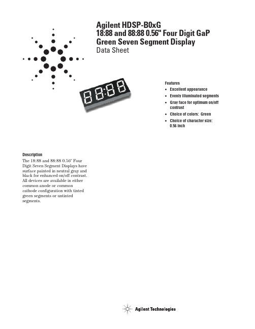
DescriptionThe 18:88 and 88:88 0.56" Four Digit Seven Segment Displays have surface painted in neutral gray and black for enhanced on/off contrast. All devices are available in either common anode or common cathode configuration with tinted green segments or untinted segments.Agilent HDSP-B0xG18:88 and 88:88 0.56" Four Digit GaP Green Seven Segment DisplayData SheetFeatures•Excellent appearance•Evenly illuminated segments•Gray face for optimum on/offcontrast•Choice of colors: Green•Choice of character size:0.56 inchFRONT SIDE2 – ∅1.70RIGHT SIDEA A A DDD C F EF E F EB CB C B C GGGDP3DP2DIGIT 2DIGIT 3DIGIT 4DIGIT 1AF EB G D NOTE:ALL DIMENSIONS ARE IN MILLIMETERS (INCHES).UNLESS OTHERWISE STATED, TOLERANCES ARE ± 0.25 mm.Pin Configuration Function Pin HDSP-B01G/B03G/B05G/B07G/B09G HDSP-B02G/B04G/B06G/B08G/B10G 1Anode E Cathode E 2Anode D Cathode D 3Anode DP Cathode DP 4Anode C Cathode C 5Anode GCathode G6Digit 4 Common Cathode Digit 4 Common Anode 7Anode BCathode B8Digit 3 Common Cathode Digit 3 Common Anode 9Digit 2 Common Cathode Digit 2 Common Anode 10Anode F Cathode F 11Anode ACathode A12Digit 1 Common CathodeDigit 1 Common AnodeFRONT SIDE2 – ∅1.70RIGHT SIDEAA A DDD B CF EF E F EB CB C B C GGGDP3DP2DIGIT 2DIGIT 3DIGIT 4DIGIT 1NOTE:ALL DIMENSIONS ARE IN MILLIMETERS (INCHES).UNLESS OTHERWISE STATED, TOLERANCES ARE ± 0.25 mm.HDSP-B01G and HDSP-B05G (Common Cathode)HDSP-B02G and HDSP-B06G (Common Anode)DIGIT 1DIGIT 2DIGIT 3DIGIT 4A 11B 7C 4D 2E 1F 10G 5DP 3DIGIT 1DIGIT 2DIGIT 3DIGIT 4A 11B 7C 4D 2E 1F 10G 5DP 3HDSP-B03G, HDSP-B07G, and HDSP-B09G (Common Cathode)HDSP-B04G, HDSP-B08G, and HDSP-B10G (Common Anode)DIGIT 1DIGIT 2DIGIT 3DIGIT 4A 11B 7C 4D 2E 1F 10G 5DP3DIGIT 1DIGIT 2DIGIT 3DIGIT 4A 11B 7C 4D 2E 1F 10G 5DP 3DevicesHDSP-DescriptionB01G88:88 0.56" Green 4 Digit, Tinted Green, Common Cathode, Display 18:88, Gray Color Surface B02G88:88 0.56" Green 4 Digit, Tinted Green, Common Anode, Display 18:88, Gray Color Surface B03G88:88 0.56" Green 4 Digit, Tinted Green, Common Cathode, Display 88:88, Gray Color Surface B04G88:88 0.56" Green 4 Digit, Tinted Green, Common Anode, Display 88:88, Gray Color Surface B05G88:88 0.56" Green 4 Digit, Untinted, Common Cathode, Display 18:88, Gray Color SurfaceB06G88:88 0.56" Green 4 Digit, Untinted, Common Anode, Display 18:88, Gray Color SurfaceB07G88:88 0.56" Green 4 Digit, Untinted, Common Cathode, Display 88:88, Gray Color SurfaceB08G88:88 0.56" Green 4 Digit, Untinted, Common Anode, Display 88:88, Gray Color SurfaceB09G88:88 0.56" Green 4 Digit, Untinted, Common Cathode, Display 88:88, Black Color SurfaceB10G88:88 0.56" Green 4 Digit, Untinted, Common Anode, Display 88:88, Black Color SurfacePart Numbering System5082 -X X X X-X X X X XHDSP-X X X X-X X X X XMechanical Options[1]00: No Mechanical OptionColor Bin Options[1,2]0: No Color Bin LimitationMaximum Intensity Bin[1,2]0: No Maximum Intensity Bin LimitationMinimum Intensity Bin[1,2]0: No Minimum Intensity Bin LimitationDevice Configuration/Color[1]G: GreenDevice Specific Configuration[1]Refer to Respective DatasheetPackage[1]Refer to Respective DatasheetNotes:1. For codes not listed in the figure above, please refer to the respective datasheet or contactyour nearest Agilent representative for details.2. Bin options refer to shippable bins for a part number. Color and Intensity Bins are typicallyrestricted to 1 bin per tube (exceptions may apply). Please refer to respective datasheet forspecific bin limit information.Electrical/Optical Characteristics at T A = 25˚C Device Series HDSP-ParameterSymbol Min.Typ.Max.Units Test Conditions Luminous Intensity/SegmentI V20003200µcd I F = 10 mA(Digit Average)32004500All DevicesForward Voltage/Segment or DP V F 1.802.20 2.60V I F = 20 mA Peak Wavelength λPEAK 568nm I F = 20 mA Dominant Wavelength λd 573nmI F = 20 mA Luminous Intensity I V-M 2:1I F = 10 mA Matching Ratio Reverse CurrentI R100µAV R = 5 VNotes:1.Typical specification for reference only. Do not exceed absolute maximum ratings.2.The dominant wavelength, λd , is derived from the CIE chromaticity diagram and is that single wavelength which defines the color of the device.Absolute Maximum RatingsDescriptionGreen Units Average Power per Segment or DP65mW Peak Forward Current per Segment or DP 100mA DC Forward Current per Segment or DP 25mA Operating Temperature Range–40 to +105˚C Storage Temperature Range–40 to +105˚C Reverse Voltage per Segment or DP5V Wavesoldering Temperature for 3 seconds 2 mm below body250˚CNote:1.Derate above 40˚C at 0.33 mA/˚C for green.B01G, B02G, B03G, B04G B05G, B06G, B07G, B08G,B09G, B10G Intensity Bin Limits (µcd at 10 mA)Device Series HDSP-B01G, B02G, B03G, B04G B05G, B06G, B07G, B08G, B09G, B10GBin Name Min.[1]Max.[1]Min.[1]Max.[1]K 20003200NA NA L 3200505032005050MNA NA50508000Note:1.Tolerance for each bin limit is ±10%.Color Categories (Tolerance ± 1 nm)Rank Symbol Hue Range Unit 22573.5–576.5nm 33570.5–573.5nmContrast EnhancementFor information on contrast enhancement, please see Application Note 1015.Soldering/CleaningCleaning agents from the ketone family (acetone, methyl ethyl ketone, etc.) and from thechlorinated hydrocarbon family (methylene chloride,trichloroethylene, carbon tetrachloride, etc.) are notrecommended for cleaning LED parts. All these various solvents attack or dissolve theencapsulating epoxies used to form the package of plastic LED parts.Figure 1. Maximum allowable DC current vs.ambient temperature.Figure 2. Forward current vs. forward voltage.Figure 3. Relative luminous intensity vs. DC forward current.Figure 4. Relative efficiency (luminous intensity per unit current) vs. peak current.I D C – M A X I M U M D C C U R R E N T P E R S E G M E N T – m AT A – AMBIENT TEMPERATURE – °CI F – F O R W A R D C U R R E N T P E R S E G M E NT – m AV F – FORWARD VOLTAGE – VR E L A T I V E L U M I N O U S I N T E N S I T Y (N O R M A L I Z E D T O 1 A T 10 mA F O R G R E E N )I F – DC FORWARD CURRENT – mA8642R E L A T I V E E F F I C I E N C Y (N O R M A L I Z E D T O 1 A T 10 m A )1.4005101520253035404550PEAK FORWARD CURRENTPER SEGMENT – mA/semiconductorsFor product information and a complete list of distributors, please go to our web site.For technical assistance call:Americas/Canada: +1 (800) 235-0312 or (916) 788-6763Europe: +49 (0) 6441 92460China: 10800 650 0017Hong Kong: (+65) 6756 2394India, Australia, New Zealand: (+65) 6755 1939Japan: (+81 3) 3335-8152(Domestic/Interna-tional), or 0120-61-1280(Domestic Only)Korea: (+65) 6755 1989Singapore, Malaysia, Vietnam, Thailand,Philippines, Indonesia: (+65) 6755 2044Taiwan: (+65) 6755 1843Data subject to change.Copyright © 2004 Agilent Technologies, Inc.Obsoletes 5988-5381EN June 30, 20045988-7859EN。
5082-7401-EHZ00中文资料

7.6 mm (0.3 inch) Micro Bright Seven Segment Displays Technical DataFeatures• Available with Colon for Clock Display • Compact Package 0.300 x 0.500 inchesLeads on 2.54 mm (0.1 inch)Centers• Choice of Colors AlGaAs Red, HighEfficiency Red, Yellow, Green,Orange• Excellent Appearance Evenly Lighted Segments Mitered Corners on Segments Surface Color Gives Optimum Contrast±50° Viewing Angle • Design FlexibilityCommon Anode or Common CathodeRight Hand Decimal Point ±1. Overflow Character • Categorized for Luminous IntensityYellow and Green Categorized for ColorUse of Like Categories Yields a Uniform Display • High Light Output • High Peak Current• Excellent for Long Digit String Multiplexing • Intensity and Color Selection Available See Intensity and ColorSelected Displays Data Sheet • Sunlight Viewable AlGaAsDescriptionThe 7.6 mm (0.3 inch) LED seven segment displays are designed for viewing distances up to 3 metres (10 feet). These devices use an industry standard size package and pinout. Both the numeric andDevicesOrange AlGaAs [1]HER [1]Yellow [1]Green [1]Package HDSP-HDSP-HDSP-HDSP-HDSP- DescriptionDrawingA401A151750174017801Common Anode Right A Hand Decimal750274027802Common Anode Right Hand B Decimal, Colon A403A153750374037803Common Cathode Right C Hand Decimal750474047804Common Cathode Right Hand D Decimal, ColonA157750774077807Common Anode ±1. Overflow E A158750874087808Common Cathode ±1. OverflowFNote:1. These displays are recommended for high ambient light operation. Please refer to the HDSP-A10X AlGaAs, HDSP-335X HER, HDSP-A80X Yellow, and HDSP-A90X Green data sheet for low current operation.HDSP-740x Series HDSP-750x Series HDSP-780x Series HDSP-A15x Series HDSP-A40x Series±1. overflow devices feature a right hand decimal point. All devices are available as either common anode or common cathode.These displays are ideal for most applications. Pin for pin equiv-alent displays are also available in a low current design. The low current displays are ideal forportable applications. For additional information see the Low Current Seven Segment Displays.Part Numbering SystemNotes:1. For codes not listed in the figure above, please refer to the respective datasheet or contact your nearest Agilent representative for details.2. Bin options refer to shippable bins for a part number. Color and Intensity Bins are typically restricted to 1bin per tube (exceptions may apply). Please refer to respective datasheet for specific bin limit information.5082 -X X X X-X X X X X HDSP-X X X X-X X X X XMechanical Options [1]00: No Mechanical OptionColor Bin Options [1,2]0: No Color Bin Limitation3: Color Bins 3- and 3+ only (applicable for Yellow devices only)Z: Color Bins 2- and 3+ only (applicable for Yellow devices only)Maximum Intensity Bin [1,2]0: No Maximum Intensity Bin Limitation Minimum Intensity Bin [1,2]0: No Minimum Intensity Bin Limitation Device Configuration/Color [1]1: Common Anode 2: Common Anode 3: Common Cathode 4: Common CathodeDevice Specific Configuration [1]Refer to Respective DatasheetPackage [1]A: 7.6 mm (0.3 inch) Single Digit Seven Segment DisplayPackage Dimensions NOTES:1. ALL DIMENSIONS IN MILLIMETRES (INCHES).2. MAXIMUM.3. ALL UNTOLERANCED DIMENSIONS AREFOR REFERENCE ONLY.4. REDUNDANT ANODES.5. REDUNDANT CATHODES.6. FOR HDSP-7400/-7800 SERIES PRODUCT ONLY.Device Series HDSP-ParameterSymbol Min.Typ.Max.Units Test Conditions Luminous Intensity/Segment [1,2,5]I V6.914.0mcd I F = 20 mA (Digit Average)1.8VI F = 20 mAForward Voltage/Segment or DPV F2.03.0V I F = 100 mAA15xPeak Wavelength λPEAK 645nm Dominant Wavelength [3]λd 637nm Reverse Voltage/Segment or DP [4]V R 3.015.0V I R = 100 µA Temperature Coefficient of ∆V F /°C -2mV/°C V F /Segment or DPThermal Resistance LED Junction-R θJ-PIN255°C/W/Segto-PinAlGaAs RedElectrical/Optical Characteristics at T A = 25°C Absolute Maximum RatingsAlGaAs Red HER/Orange Yellow GreenHDSP-A150HDSP-7500/-A40X HDSP-7400HDSP-7800DescriptionSeriesSeries SeriesSeriesUnits Average Power per Segment or DP 9610580105mW Peak Forward Current per 160[1]90[3]60[5]90[7]mA Segment or DPDC Forward Current per 40[2]30[4]20[6]30[8]mASegment or DPOperating Temperature Range –20 to +100[9]–40 to +100°CStorage Temperature Range –55 to +100°C Reverse Voltage per Segment or DP 3.0V Lead Solder Temperature for 3Seconds (1.59 mm [0.063 in.] 260°Cbelow seating plane)Notes:1. See Figure 1 to establish pulsed conditions.2. Derate above 46°C at 0.54 mA/°C.3. See Figure 6 to establish pulsed conditions.4. Derate above 53°C at 0.45 mA/°C.5. See Figure 7 to establish pulsed conditions.6. Derate above 81°C at 0.52 mA/°C.7. See Figure 8 to establish pulsed conditions.8. Derate above 39°C at 0.37 mA/°C.9. For operation below –20°C, contact your local Agilent components sales office or an authorized distributor.High Efficiency RedDeviceSeriesHDSP-Parameter Symbol Min.Typ.Max.Units Test Conditions Luminous Intensity/Segment[1,2,6]360980I F = 5 mA(Digit Average)I Vµcd5390I F = 20 mA Forward Voltage/Segment or DP V F 2.0 2.5V I F = 20 mA 750x Peak WavelengthλPEAK635nmDominant Wavelength[3]λd626nmReverse Voltage/Segment or DP[4]V R 3.030V I R = 100 µATemperature Coefficient of∆V F/°C-2mV/°CV F/Segment or DPThermal Resistance LED Junction-RθJ-PIN200°C/W/Segto-PinOrangeDeviceSeriesHDSP-Parameter Symbol Min.Typ.Max.Units Test Conditions Luminous Intensity/Segment[1,2,6]I V0.70mcd I F = 5 mA(Digit Average)Forward Voltage/Segment or DP V F 2.0 2.5V I F = 20 mA A40x Peak WavelengthλPEAK600nmDominant Wavelength[3]λd603nmReverse Voltage/Segment or DP[4]V R 3.030V I R = 100 µATemperature Coefficient of∆V F/°C-2mV/°CV F/Segment or DPThermal Resistance LED Junction-RθJ-PIN200°C/W/Segto-PinYellowDeviceSeriesHDSP-Parameter Symbol Min.Typ.Max.Units Test Conditions Luminous Intensity/Segment[1,2,7]225480I F = 5 mA(Digit Average)I Vµcd2740I F = 20 mA Forward Voltage/Segment or DP V F 2.2 2.5V I F = 20 mA 740x Peak WavelengthλPEAK583nmDominant Wavelength[3,9]λd581.5586592.5nmReverse Voltage/Segment or DP[4]V R 3.050.0V I R = 100 µATemperature Coefficient of∆V F/°C-2mV/°CV F/Segment or DPThermal Resistance LED Junction-RθJ-PIN200°C/W/Segto-PinHigh Performance GreenDeviceSeriesHDSP-Parameter Symbol Min.Typ.Max.Units Test Conditions Luminous Intensity/Segment[1,2,8]8603000I F = 10 mA(Digit Average)I Vµcd6800I F = 20 mA Forward Voltage/Segment or DP V F 2.1 2.5V I F = 10 mA 780x Peak WavelengthλPEAK566nmDominant Wavelength[3,9]λd571577nmReverse Voltage/Segment or DP[4]V R 3.050.0V I R = 100 µATemperature Coefficient of∆V F/°C-2mV/°CV F/Segment or DPThermal Resistance LED Junction-RθJ-PIN200°C/W/Segto-PinNotes:1. Case temperature of device immediately prior to the intensity measurement is 25°C.2. The digits are categorized for luminous intensity. The intensity category is designated by a letter on the side of the package.3. The dominant wavelength, λd, is derived from the CIE chromaticity diagram and is that single wavelength which defines the color ofthe device.4. Typical specification for reference only. Do not exceed absolute maximum ratings.5. For low current operation the AlGaAs HDSP-A101 series displays are recommended.6. For low current operation the HER HDSP-7511 series displays are recommended.7. For low current operation the Yellow HDSP-A801 series displays are recommended.8. For low current operation the Green HDSP-A901 series displays are recommended.9. The yellow (HDSP-7400) and Green (HDSP-7800) displays are categorized for dominant wavelength. The category is designated by anumber adjacent to the luminous intensity category letter.AlGaAs Redt – PULSE DURATION – µs P101100R A T I O O F M A X I M U M O P E R A T I N G P E A K C U R R E N T T O T E M P E R A T U R E D E R A T E D M A X I M U M D C C U R R E N TI P E A K F I M A X DC Figure 4. Relative Luminous Intensity vs. DC Forward Current.Figure 2. Maximum Allowable DC Current per Segment as a Function of Ambient Temperature.Figure 1. Maximum Allowed Peak Current vs.Pulse Duration – AlGaAs Red.Figure 5. Relative Efficiency (LuminousIntensity per Unit Current) vs. Peak Current.Figure 3. Forward Current vs.Forward Voltage.T A – AMBIENT TEMPERATURE – °C I D C M A X . – M A X I M U M D C C U R R E N T P E R S E G M E N T– m AV F – FORWARD CURRENT – VI F – F O R W A R D C U R R E N T P E R S E G M E N T – m AI PEAK – PEAK FORWARD CURRENT PER SEGMENT – mAηP E A K – N O R M A L I Z E D R E L A T I V E E F F I C I E N C YI F – FORWARD CURRENT PER SEGMENT – mA R E L A T I V E L U M I N O U S I N T E N S I T Y (N O R M A L I Z E D T O 1 A T 20 m A )Figure 12. Relative Efficiency (Luminous Intensity per Unit Current) vs. Peak Current.ηP E A K – R E L A T I V E E F F I C I E N C Y (N O R M A L I Z E D T O 1 A T 5 m A F O R H E R ,O R A N G E A N D Y E L L O W , A N D 10 m A F O R G R E E N )I PEAK – PEAK FORWARD CURRENTPER SEGMENT – mAHER, Yellow, Green, OrangeFigure 6. Maximum Tolerable Peak Current vs.Pulse Duration – HER, Orange.Figure 7. Maximum Tolerable Peak Current vs. Pulse Duration – Yellow.Figure 10. Forward Current vs.Forward Voltage Characteristics.Figure 11. Relative LuminousIntensity vs. DC Forward Current.Figure 8. Allowable Peak Current vs.Pulse Duration – Green.Figure 9. Maximum Allowable DC Current per Segment as a Function of Ambient Temperature.R A T I O O F M A X I M U M O P E R A T I N G P E A K C U R R E N T T O T E M P E R A T U R E D E R A T E D D C C U R R E N TI P E A K F I M A X D C t – PULSE DURATION – µs P 101100DCR A T I O O F M A X I M U M O P E R A T I N G P E A K C U R R E N T T O T E M P E R A T U R E D E R A T E D D C C U R R E N TI P E A K FI M A X D C t – PULSE DURATION – µs P101100R A T I O O F M A X I M U M O P E R A T I N G P E A K C U R R E N T T O T E M P E R A T U R E D E R A T E D D C C U R R E N TI P E A K FI M A X D C t – PULSE DURATION – µs P10110040051015202530352010090807060504030T – AMBIENT TEMPERATURE – °C AI M A X –M A X I M U M D C C U R R E N T P E R S E G M E N T – m AD C120110504510080604020I – F O R W A R D C U R R E N T P E R S E G M E N T – m A FV – FORWARD VOLTAGE – V F R E L A T I V E L U M I N O U S I N T E N S I T Y (N O R M A L I Z E D T O 1 A T 5 m A F O R H E R A N D )t (Y E L L O W A N D T O1 A T 10 m A F O R G R E E N )1510205301025I – FORWARD CURRENT PER SEGMENT – mA FHDSP-A15x IV Bin Category Min.Max.M 7.0713.00N 10.6019.40O 15.9029.20P 23.9043.80Q 35.8065.60Intensity Bin Limits (mcd)AlGaAs RedHDSP-750x IV Bin Category Min.Max.B 0.3420.630C 0.5160.946D 0.774 1.418E 1.160 2.127F 1.740 3.190G 2.610 4.785H 3.9157.177HERHDSP-740x IV Bin Category Min.Max.B 0.2290.387C 0.3170.582D 0.4760.872E 0.714 1.311F 1.073 1.967G 1.609 2.950H 2.4134.425YellowHDSP-780x IV Bin Category Min.Max.H 0.86 1.58I 1.29 2.37J 1.94 3.55K 2.90 5.33L 4.378.01GreenOrangeHDSP-A40XIV Bin Category Min.Max.A 0.2840.433B 0.3540.541C 0.4430.677D 0.5540.846E 0.692 1.057F 0.856 1.322G 1.082 1.652H 1.352 2.066I 1.692 2.581J 2.114 3.227K 2.641 4.034L 3.300 5.042M 4.127 6.303N 5.1577.878Color CategoriesNote:All categories are established for classification of products. Products may not be available in all categories. Please contact your Agilent representatives for further clarification/information.Contrast EnhancementFor information on contrastenhancement, please seeApplication Note 1015.Soldering/CleaningCleaning agents from the ketonefamily (acetone, methyl ethylketone, etc.) and from thechlorinated hydrocarbon family(methylene chloride, trichloro-ethylene, carbon tetrachloride,etc.) are not recommended forcleaning LED parts. All of thesevarious solvents attack or dissolvethe encapsulating epoxies used toform the package of plastic LEDparts.For further information onsoldering LEDs, please refer toApplication Note 1027.元器件交易网/semiconductorsFor product information and a complete list ofdistributors, please go to our web site.For technical assistance call:Americas/Canada: +1 (800) 235-0312 or(408) 654-8675Europe: +49 (0) 6441 92460China: 10800 650 0017Hong Kong: (+65) 271 2451India, Australia, New Zealand: (+65) 271 2394Japan: (+81 3) 3335-8152(Domestic/Interna-tional), or 0120-61-1280(Domestic Only)Korea: (+65) 271 2194Malaysia, Singapore: (+65) 271 2054Taiwan: (+65) 271 2654Data subject to change.Copyright © 2002 Agilent Technologies, Inc.Obsoletes 5988-0382ENFebruary 11, 20025988-4434EN。
5082-E156-OL000资料

Features• Industry Standard Size • Industry Standard Pinout7.62 mm (0.300 inch) DIP Leads on 2.54 mm (0.100 inch) Centers • Choice of ColorsAlGaAs Red, High Efficiency Red,Yellow, Green• Excellent Appearance Evenly Lighted Segments ±50° Viewing AngleOptimum Contrast Given byGray Top Surface for AlGaAs Red and Green DevicesRed Top Surface for HER Devices Yellow Top Surface for Yellow Devices• Design Flexibility Common Anode or Common Cathode Single DigitsLeft or Right Hand Decimal Point ±1. Overflow Character• Categorized for Luminous IntensityYellow and Green Categorized for ColorUse of Like Categories Yields a Uniform Display • High Light Output • High Peak Current• Excellent for Long Digit String Multiplexing• Intensity and Color Selection AvailableSee Intensity and Color Selected Displays Data Sheet• Sunlight Viewable AlGaAsAlGaAs [1]HER [1]Yellow Green Package Red HDSP-5082-5082-HDSP-DescriptionDrawing7610762036007.6 mm Common Anode Left Hand Decimal A 7611762136017.6 mm Common Anode Right Hand Decimal B 7613762336037.6 mm Common Cathode Right Hand Decimal C 7616762636067.6 mm Universal ±1. Overflow Right Hand Decimal [2]D E15076507660460010.9 mm Common Anode Left Hand Decimal E E15176517661460110.9 mm Common Anode Right Hand Decimal F E15376537663460310.9 mm Common Cathode Right Hand Decimal G E15676567666460610.9 mm Universal ±1. Overflow Right Hand Decimal [2]HNotes:1. These displays are recommended for high ambient light operation. Please refer to the HDSP-E10X AlGaAs and HDSP-335X HER data sheet for low current operation.2. Universal pinout brings the anode and cathode of each segment’s LED out to separate pins. See internal diagram D.3. Universal pinout brings the anode and cathode of each segment’s LED out to separate pins. See internal diagram H.Devices5082-761x Series 5082-762x Series 5082-765x Series 5082-766x Series HDSP-360x Series HDSP-460x Series HDSP-E15x Series7.6 mm (0.3 inch)/10.9 mm (0.43 inch) Seven Segment Displays Technical DataDescriptionThe 7.6 mm (0.3 inch) and 10.9mm (0.43 inch) LED sevensegment displays are designed for viewing distances up to 3 metres (10 feet) and 5 metres (16 feet).These devices use an industry standard size package andpinouts. All devices are available as either common anode or common cathode.Part Numbering System5082 -X X X X-X X X X XHDSP-X X X X-X X X X XMechanical Options[1]00: No Mechanical OptionColor Bin Options[1,2]0: No Color Bin Limitation4: Color Bin 4 Only (applicable for Green devices only)B: Color Bins 2 and 3 (applicable for Yellow devices only)Maximum Intensity Bin[1,2]0: No Maximum Intensity Bin LimitationMinimum Intensity Bin[1,2]0: No Minimum Intensity Bin LimitationDevice Configuration/Color[1]0: Common Anode1: Common Anode3: Common CathodeDevice Specific Configuration[1]Refer to Respective DatasheetPackage[1]E: 10.9 mm (0.43 inch) Single Digit Seven Segment Display Notes:1. For codes not listed in the figure above, please refer to the respective datasheet or contact your nearestAgilent representative for details.2. Bin options refer to shippable bins for a part number. Color and Intensity Bins are typically restricted to 1bin per tube (exceptions may apply). Please refer to respective datasheet for specific bin limit information.displays are ideal for portable applications. The high light ambient displays are ideal for high light ambients or long string lengths. For additional informa-tion see the Low Current Seven Segment Displays, or High Light Ambient Seven Segment Displays data sheets.NOTES;1. DIMENSIONS IN MILLIMETRES AND (INCHES).2. ALL UNTOLERANCED DIMENSIONS ARE FOR REFERENCE ONLY.3. REDUNDANT ANODES.4. UNUSED DP POSITION.5. SEE INTERNALCIRCUIT DIAGRAM.6. REDUNDANT CATHODE.7. SEE PART NUMBER TABLE FOR L.H.D.P.AND R.H.D.P.DESIGNATION.8. FOR YELLOW AND GREEN DEVICES ONLY.Package DimensionsThese displays are ideal for most applications. Pin for pin equiva-lent displays are also available in a low current or high lightambient design. The low currentInternal Circuit DiagramAbsolute Maximum RatingsAlGaAs Red HER Yellow GreenHDSP-E1505082-7610/5082-7620/HDSP-3600/ Description Series7650 Series7660 Series4600 Series Units Average Power per Segment or DP9610580105mW Peak Forward Current per160[1]90[3]60[5]90[7]mA Segment or DPDC Forward Current per40[2]30[4]20[6]30[8]mA Segment or DPOperating Temperature Range-20 to +100[9]-40 to +100°C Storage Temperature Range -55 to +100°C Reverse Voltage per 3.0V Segment or DPWave Soldering Temperature for3 Seconds (1.59 mm [0.063 in.] 250°Cbelow Body)Notes:1.See Figure 1 to establish pulsed conditions.2. Derate above 46°C at 0.54 mA/°C.3. See Figure 6 to establish pulsed conditions.4. Derate above 53°C at 0.45 mA/°C.5. See Figure 7 to establish pulsed conditions.6. Derate above 81°C at 0.52 mA/°C.7. See Figure 8 to establish pulsed conditions.8. Derate above 39°C at 0.37 mA/°C.9. For operation below -20°C, contact your local Agilent components sales office or an authorized distributor.Electrical/Optical Characteristics at T A = 25°CAlGaAs RedDeviceSeries Parameter Symbol Min.Typ.Max.Units Test Conditions Luminous Intensity/Segment[1,2,5]I V8.515.0mcd I F = 20 mA(Digit Average)1.8V I F = 20 mAForward Voltage/Segment or DP V F2.03.0V I F = 100 mAHDSP-E15x Peak WavelengthλPEAK645nmDominant Wavelength[3]λd637nmReverse Voltage/Segment or DP[4]V R 3.015V I R = 100 µATemperature Coefficient of∆V F/°C-2mV/°CV F/Segment or DPThermal Resistance LED Junction-RθJ-PIN340°C/W/Segto-PinHigh Efficiency RedDeviceSeries Parameter Symbol Min.Typ.Max.Units Test Conditions 5082-761x Luminous Intensity/Segment[1,2,6]340800µcd I F = 5 mA (Digit Average)I V5082-765x3401115µcd I F = 5 mA Forward Voltage/Segment or DP V F 2.1 2.5V I F = 20 mAPeak WavelengthλPEAK635nmDominant Wavelength[3]λd626nm AllReverse Voltage/Segment or DP[4]V R 3.030V I R = 100 µATemperature Coefficient of∆V F/°C-2mV/°CV F/Segment or DPThermal Resistance LED RθJ-PIN280°C/WJunction-to-PinDevice Series ParameterSymbol Min.Typ.Max.Units Test Conditions 5082-762x Luminous Intensity/Segment [1,2]205620µcdI F = 5 mA(Digit Average)I V5082-766x290835µcd I F = 5 mA Forward Voltage/Segment or DP V F 2.2 2.5V I F = 20 mAPeak WavelengthλPEAK 583nm Dominant Wavelength [3,7]λd 581.5586592.5nm AllReverse Voltage/Segment or DP [4]V R 3.040V I R = 100 µA Temperature Coefficient of ∆V F /°C -2mV/°C V F /Segment or DP Thermal Resistance LED R θJ-PIN280°C/W/SegJunction-to-PinYellowNotes:1. Device case temperature is 25°C prior to the intensity measurement.2. The digits are categorized for luminous intensity. The intensity category is designated by a letter on the side of the package.3. The dominant wavelength, λd , is derived from the CIE chromaticity diagram and is that single wavelength which defines the color of the device.4. Typical specification for reference only. Do not exceed absolute maximum ratings.5. For low current operation, the AlGaAs HDSP-E10X series displays are recommended. They are tested at 1 mA dc/segment and are pin for pin compatible with the HDSP-E15X series.6. For low current operation, the HER HDSP-335X series displays are recommended. They are tested at 2 mA dc/segment and are pin for pin compatible with the 5082-7650 series.7. The Yellow (5082-7620/7660) and Green (HDSP-3600/4600) displays are categorized for dominant wavelength. The category is designated by a number adjacent to the luminous intensity category letter.High Performance GreenDevice Test Series ParameterSymbol Min.Typ.Max.Units Conditions HDSP-360x Luminous Intensity/Segment [1,2]8602700µcdI F = 10 mA(Digit Average)I VHDSP-460x10304000µcd I F = 10 mA Forward Voltage/Segment or DP V F 2.1 2.5V I F = 10 mAPeak WavelengthλPEAK 566nm Dominant Wavelength [3,7]λd 571577nm AllReverse Voltage/Segment or DP [4]V R 3.050V I R = 100 µA Temperature Coefficient of ∆V F /°C -2mV/°C V F /Segment or DP Thermal Resistance LED R θJ -PIN280°C/W/SegJunction-to-PinFigure 3. Forward Current vs. Forward Voltage.Figure 2. Maximum Allowable DC Current vs.Ambient Temperature.Figure 4. Relative Luminous Intensity vs. DC Forward Current.Figure 5. Relative Efficiency (Luminous Intensity per Unit Current) vs. Peak Current.AlGaAs RedI D C M A X . – M A X I M U M D C C U R R E N T P E R S E G M E N T – m AT A – AMBIENT TEMPERATURE – °C5030102051525354045I F – F O R W A R D C U R R E N T P E R S E G M E N T – m AV F – FORWARD VOLTAGE – V R E L A T I V E L U M I N O U S I N T E N S I T Y (N O R M A L I Z E D T O 1 A T 20 m A )0I F – FORWARD CURRENT PER SEGMENT – mA2.001.501.250.750.2520401.751.000.5010305152535ηP E A K – N O R M A L I Z E D R E L A T I V E EF F I C I E N C Y0.5I PEAK – PEAK FORWARD CURRENTPER SEGMENT – mA50.0150.05.0HER, Yellow, GreenFigure 8. Allowable Peak Current vs.Pulse Duration – Green Series.Figure 9. Maximum Allowable DC Current vs.Ambient Temperature.Figure 11. Relative LuminousIntensity vs. DC Forward Current.Figure 10. Forward Current vs.Forward Voltage.Figure 12. Relative LuminousEfficiency (Luminous Intensity per Unit Current) vs. Peak Current.HDSP-E15x IV Bin Category Min.Max.L 8.6715.90M 13.0023.80N 19.5035.80O 29.3053.60P 43.9080.50Intensity Bin Limits (mcd)AlGaAs RedHER5082-761x IV Bin Category Min.Max.B 0.3690.630C 0.5160.946D 0.774 1.418E 1.160 2.127F 1.740 3.190G 2.610 4.785H 3.9157.1775082-765xIV Bin Category Min.Max.B 0.3470.593C 0.4850.890D 0.728 1.333E 1.091 2.000F 1.636 3.000G 2.454 4.500H 3.6826.751Yellow5082-762x IV Bin Category Min.Max.B 0.2290.387C 0.3170.582D 0.4760.872E 0.714 1.311F 1.073 1.967G 1.609 2.950H 2.413 4.4255082-766xIV Bin Category Min.Max.C 0.2970.543D 0.4450.817E 0.669 1.225F 1.003 1.838G 1.504 2.758H 2.2564.137HDSP-460xIV Bin Category Min.Max.G 1.03 1.88H 1.54 2.82I 2.31 4.23J 3.46 6.34K 5.189.50L 7.7814.26GreenHDSP-360x IV Bin Category Min.Max.H 0.86 1.58I 1.29 2.37J 1.94 3.55K 2.90 5.33L 4.378.01Color CategoriesNote:All categories are established for classification of products. Products may not be available in all categories. Please contact your Agilent representatives for further clarification/information.Contrast EnhancementFor information on contrastenhancement, please seeApplication Note 1015.Soldering/CleaningFor information on solderingLEDs, please refer to ApplicationNote 1027.元器件交易网/semiconductorsFor product information and a complete list ofdistributors, please go to our web site.For technical assistance call:Americas/Canada: +1 (800) 235-0312 or(916) 788-6763Europe: +49 (0) 6441 92460China: 10800 650 0017Hong Kong: (+65) 6756 2394India, Australia, New Zealand: (+65) 6755 1939Japan: (+81 3) 3335-8152 (Domestic/Interna-tional), or 0120-61-1280 (Domestic Only)Korea: (+65) 6755 1989Singapore, Malaysia, Vietnam, Thailand,Philippines, Indonesia: (+65) 6755 2044Taiwan: (+65) 6755 1843Data subject to change.Copyright © 2004 Agilent Technologies, Inc.Obsoletes 5963-7394EJuly 17, 20045988-3325EN。
5082-5523-FK000中文资料
14.2 mm (0.56 inch)Seven Segment Displays Technical DataFeatures• Industry Standard Size • Industry Standard Pinout 15.24 mm (0.6 in.) DIP Leads on 2.54 mm (0.1 in.) Centers • Choice of ColorsAlGaAs Red, High Efficiency Red, Yellow, Green, Orange • Excellent Appearance Evenly Lighted Segments Mitered Corners on Segments Gray Package Gives Optimum Contrast±50° Viewing Angle • Design FlexibilityCommon Anode or Common CathodeSingle and Dual Digits Right Hand Decimal Point ±1. Overflow Character• Categorized for Luminous IntensityYellow and Green Categorized for ColorUse of Like Categories Yields a Uniform Display • High Light Output • High Peak Current• Excellent for Long Digit String Multiplexing • Intensity and Color Selection OptionSee Intensity and ColorSelected Displays Data Sheet • Sunlight Viewable AlGaAsDescriptionThe 14.2 mm (0.56 inch) LED seven segment displays aredesigned for viewing distances upto 7 metres (23 feet). Thesedevices use an industry standard size package and pinout. Both the numeric and ±1 overflow devices feature a right hand decimalpoint. All devices are available as either common anode or common cathode.Orange AlGaAs Red HERYellowGreen Package HDSP-HDSP-[1]HDSP-[1]HDSP-HDSP- DescriptionDrawingH401H151550157015601Common Anode Right Hand Decimal A H403H153550357035603Common Cathode Right Hand Decimal B H157550757075607Common Anode ±1. Overflow C H158550857085608Common Cathode ±1. OverflowD K401552157215621Two Digit Common Anode Right Hand DecimalE K403552357235623Two Digit Common Cathode Right Hand DecimalFDevicesNote:1. These displays are recommended for high ambient light operation. Please refer to the HDSP-H10X/K12X AlGaAs and HDSP-555X HER data sheet for low current operation.HDSP-K40x Series HDSP-550x Series HDSP-552x Series HDSP-560x Series HDSP-562x Series HDSP-570x Series HDSP-572x Series HDSP-H15x Series HDSP-H40x SeriesThese displays are ideal for most applications. Pin for pin equivalent displays are alsoavailable in a low current design.The low current displays are idealfor portable applications. For additional information see the Low Current Seven Segment Displays data sheet.Part Numbering SystemNotes:1. For codes not listed in the figure above, please refer to the respective datasheet or contact your nearest Agilent representative for details.2. Bin options refer to shippable bins for a part number. Color and Intensity Bins are typically restricted to 1bin per tube (exceptions may apply). Please refer to respective datasheet for specific bin limit information.5082 -X X X X-X X X X X HDSP-X X X X-X X X X XMechanical Options [1]00: No Mechanical Option Color Bin Options [1,2]0: No Color Bin LimitationMaximum Intensity Bin [1,2]0: No Maximum Intensity Bin Limitation Minimum Intensity Bin [1,2]0: No Minimum Intensity Bin Limitation Device Configuration/Color [1]1: Common Anode 3: Common CathodeDevice Specific Configuration [1]Refer to Respective DatasheetPackage [1]H: 14.2 mm (0.56 inch) Single Digit Seven Segment DisplayFUNCTIONPIN AB CDEF1CATHODE e ANODE e CATHODE c ANODE cE CATHODE NO. 1 E ANODE NO. 12CATHODE d ANODE d ANODE c, d CATHODE c, d D CATHODE NO. 1 D ANODE NO. 13ANODE [3]CATHODE [4]CATHODE b ANODE bC CATHODE NO. 1 C ANODE NO. 14CATHODE c ANODE c ANODE a, b, DP CATHODE a, b, DP DP CATHODE NO. 1DP ANODE NO. 15CATHODE DP ANODE DP CATHOPDE DP ANODE DE E CATHODE NO. 1 E ANODE NO. 26CATHODE b ANODE b CATHODE a ANODE aD CATHODE NO. 2 D ANODE NO. 27CATHODE a ANODE a ANODE a, b, DP CATHODE a, b, DP G CATHODE NO. 2G ANODE NO. 28ANODE [3]CATHODE [4]ANODE c, d CATHODE c, d C CATHODE NO. 2 C ANODE NO. 29CATHODE f ANODE f CATHODE d ANODE d DP CATHODE NO. 2DP ANODE NO. 210CATHODE g ANODE g NO PINNO PINB CATHODE NO. 2 B ANODE NO. 211 A CATHODE NO. 2 A ANODE NO. 212 F CATHODE NO. 2 F ANODE NO. 213DIGIT NO. 2 ANODE DIGIT NO. 2 CATHODE 14DIGIT NO. 1 ANODE DIGIT NO. 1 CATHODE 15 B CATHODE NO. 1 B ANODE NO. 116 A CATHODE NO. 1 A ANODE NO. 117G CATHODE NO. 1G ANODE NO. 118F CATHODE NO. 1 F ANODE NO. 1NOTES:1. ALL DIMENSIONS IN MILLIMETRES (INCHES).2. ALL UNTOLERANCED DIMENSIONS ARE FOR REFERENCE ONLY.3. REDUNDANT ANODES.4. REDUNDANT CATHODES.5. FOR HDSP-5600/-5700 SERIES PRODUCT ONLY.Package DimensionsInternal Circuit DiagramNotes:1. See Figure 2 to establish pulsed conditions.2. Derate above 46°C at 0.54 mA/°C.3. See Figure 7 to establish pulsed conditions.4. Derate above 53°C at 0.45 mA/°C.5. See Figure 8 to establish pulsed conditions.HER/Orange HDSP-5500AlGaAs Red HDSP-H40x Yellow Green HDSP-H150HDSP-K40x HDSP-5700HDSP-5600 Description SeriesSeriesSeriesSeriesUnits Average Power per Segment or DP 9610580105mW Peak Forward Current per 160[1]90[3]60[5]90[7]mA Segment or DPDC Forward Current per Segment or DP 40[2]30[4]20[6]3018]mA Operating Temperature Range -20 to +100[9]-40 to +100°C Storage Temperature Range -55 to +100°C Reverse Voltage per Segment or DP 3.0V Lead Solder Temperature for 3 Seconds 260°C(1.60 mm [0.063 in.] below seating plane)Absolute Maximum Ratings6. Derate above 81°C at 0.52 mA/°C.7. See Figure 9 to establish pulsed conditions.8. Derate above 39°C at 0.37 mA/°C.9. For operation below -20°C, contact your local Agilent components sales office or an authorized distributor.Electrical/Optical Characteristics at T A = 25°CAlGaAs RedDeviceSeriesHDSP- Parameter Symbol Min.Typ.Max.Units Test Conditions Luminous Intensity/Segment[1,2,5]I V9.116.0mcd I F = 20 mA(Digit Average)1.8I F = 20 mAForward Voltage/Segment or DP V F V2.03.0I F = 100 mAH15XPeak WavelengthλPEAK645nmDominant Wavelength[3]λd637nmReverse Voltage/Segment or DP[4]V R 3.015V I R = 100 µATemperature Coefficient of∆V F/°C-2mV/°CV F/Segment or DPThermal Resistance LED Junction-RθJ-Pin400°C/W/to-Pin SegHigh Efficiency RedDeviceSeriesHDSP- Parameter Symbol Min.Typ.Max.Units Test Conditions9002800I F = 10 mA Luminous Intensity/Segment[1,2,6]I Vµcd(Digit Average)3700I F = 60 mA Peak:1 of 6 dfForward Voltage/Segment or DP V F 2.1 2.5V I F = 20 mA 55XXPeak WavelengthλPEAK635nmDominant Wavelength[3]λd626nmReverse Voltage/Segment or DP[4]V R 3.030V I R = 100 µATemperature Coefficient of∆V F/°C-2mV/°CV F/Segment or DPThermal Resistance LED Junction-RθJ-Pin345°C/W/to-Pin SegYellowDeviceSeriesHDSP- Parameter Symbol Min.Typ.Max.Units Test Conditions6001800I F = 10 mA Luminous Intensity/Segment[1,2]I Vµcd(Digit Average)2750I F = 60 mA Peak:1 of 6 dfForward Voltage/Segment or DP V F 2.1 2.5V I F = 20 mA 57XXPeak WavelengthλPEAK583nmDominant Wavelength[3,7]λd581.5586592.5nmReverse Voltage/Segment or DP[4]V R 3.040V I R = 100 µATemperature Coefficient of∆V F/°C-2mV/°CV F/Segment or DPThermal Resistance LED Junction-RθJ-Pin345°C/W/to-Pin SegOrangeDeviceSeriesHDSP- Parameter Symbol Min.Typ.Max.Units Test Conditions Luminous Intensity/Segment I V 2.37mcd I F = 10 mA(Segment Average)[1,2]Forward Voltage/Segment or DP V F 2.1 2.5V I F = 20 mAPeak WavelengthλPEAK600nm H40x Dominant Wavelength[3]λd603nm I F = 10 mA K40x Reverse Voltage/Segment or DP[4]V R 3.030V I R = 100 µA Temperature Coefficient of∆V F/°C-2mV/°CV F/Segment or DPThermal Resistance LED Junction-RθJ-Pin345°C/W/to-Pin SegDeviceSeries HDSP-ParameterSymbol Min.Typ.Max.UnitsTest Conditions 9002500I F = 10 mALuminous Intensity/Segment [1,2]I Vµcd(Digit Average)`3100I F = 60 mA Peak:1 of 6 df Forward Voltage/Segment or DPV F 2.1 2.5V I F = 10 mA56XXPeak Wavelength λPEAK 566nm Dominant Wavelength [3,7]λd 571577nm Reverse Voltage/Segment or DP [4]V R 3.050V I R = 100 µATemperature Coefficient of ∆V F /°C -2mV/°C V F /Segment or DPThermal Resistance LED Junction-R θJ-Pin345°C/W/to-PinSegHigh Performance GreenNotes:1. Device case temperature is 25°C prior to the intensity measurement.2. The digits are categorized for luminous intensity. The intensity category is designated by a letter on the side of the package.3. The dominant wavelength, λd , is derived from the CIE chromaticity diagram and is that single wavelength which defines the color of the device.4. Typical specification for reference only. Do not exceed absolute maximum ratings.5. For low current operation, the AlGaAs HDSP-H10X series displays are recommended. They are tested at 1 mA dc/segment and are pin for pin compatible with the HDSP-H15X series.6. For low current operation, the HER HDSP-555X series displays are recommended. They are tested at 2 mA dc/segment and are pin for pin compatible with the HDSP-550X series.7. The Yellow (HDSP-5700) and Green (HDSP-5600) displays are categorized for dominant wavelength. The category is designated by a number adjacent to the luminous intensity category letter.AlGaAs RedFigure 2. Maximum Tolerable Peak Current vs. Pulse Duration – AlGaAs Red.Figure 1. Maximum Tolerable Peak Current vs.Pulse Duration – Red.Figure 3. Maximum Allowable DC Current vs.Ambient Temperature.Figure 4. Forward Current vs.Forward Voltage.HER, Yellow, Green, OrangeFigure 7. Maximum Tolerable Peak Currentvs. Pulse Duration – HER, Orange.Figure 8. Maximum Tolerable Peak Current vs. Pulse Duration – Yellow.Figure 5. Relative Luminous Intensity vs. DC Forward Current.Figure 6. Relative Efficiency (Luminous Intensity per Unit Current) vs. Peak Current.I D C M A X . – M A X I M U M D C C U R R E N T P E R S E G M E N T – m AT A – AMBIENT TEMPERATURE – °C 5030102051525354045I F – F O R W A R D C U R R E N T P E R S E G M E N T – m AV F – FORWARD VOLTAGE – VR E L A T I V E L U M I N O U S I N T E N S I T Y (N O R M A L I Z E D T O 1 A T 20 m A )I F – FORWARD CURRENT PER SEGMENT – mA204010305152535ηP E A K – N O R M A L IZ E D R E L A T I V E E F F I C I E N C YI PEAK – PEAK FORWARD CURRENTPER SEGMENT – mA40051015202530352010090807060504030T – AMBIENT TEMPERATURE – °C AI M A X – M A X I M U M D C C U R R E N T P E R S E G M E N T – m AD C 4550110120Figure 11. Forward Current vs.Forward Voltage.Figure 9. Maximum Tolerable PeakCurrent vs. Pulse Duration – Green.Figure 10. Maximum Allowable DC Current vs.Ambient Temperature.Figure 12. Relative LuminousIntensity vs. DC Forward Current.Figure 13. Relative Efficiency (Luminous Intensity per Unit Current) vs. Peak Current.Electrical/OpticalFor more information onelectrical/optical characteristics,please see Application Note 1005.Contrast EnhancementFor information on contrastenhancement please see Application Note 1015.Soldering/CleaningCleaning agents from the ketone family (acetone, methyl ethyl ketone, etc.) and from thechlorinated hydrocarbon family(methylene chloride, trichloro–ethylene, carbon tetrachloride,etc.) are not recommended for cleaning LED parts. All of these various solvents attack or dissolve the encapsulating epoxies used to form the package of plastic LED parts.For information on soldering LEDs please refer to Application Note 1027.I F – F O R W A R D C U R R E N T P E R S E G M E N T – m AV F – FORWARD VOLTAGE – VR E L A T I V E L U M I N O U S I N T E N S I T Y (N O R M A L I Z E D A T 10 m A )I F – DC FORWARD CURRENT – mAηV – R E L A T I V E E F F I C I E N C Y (N O R M A L I Z E D T O 1 A T 10 m A P E R S E G M EN T )0.6I PEAK – PEAK FORWARD CURRENTPER SEGMENT – mA902070801001.61.41.31.10.90.860504030100.71.01.21.5HDSP-H15x IV Bin Category Min.Max.K 9.2016.90L 13.8025.30M 20.7038.00N 31.1056.90O 46.6085.40Intensity Bin Limits (mcd)AlGaAs RedHDSP-550x/552x IV Bin Category Min.Max.E 0.91 1.67F 1.37 2.51G 2.05 3.76H 3.08 5.64I 4.628.64J 6.9312.70K 10.3919.04HERHDSP-570x/572xIV Bin Category Min.Max.D 0.61 1.11E 0.91 1.67F 1.37 2.51G 2.05 3.76H 3.08 5.64I 4.628.64J 6.9312.70K 10.3919.04YellowHDSP-560x/562x IV Bin Category Min.Max.E 0.91 1.67F 1.37 2.51G 2.05 3.76H 3.08 5.64I 4.618.46GreenColor CategoriesNote:All categories are established for classification of products. Products may not be available in all categories. Please contact your Agilent representatives for further clarification/information.10HDSP-H40x/K40x IV Bin Category Min.Max.B 0.77 1.17C 0.95 1.45D 1.19 1.82E 1.49 2.27F 1.85 2.89G 2.32 3.54H 2.904.43Orange元器件交易网元器件交易网/semiconductorsFor product information and a complete list ofdistributors, please go to our web site.For technical assistance call:Americas/Canada: +1 (800) 235-0312 or(408) 654-8675Europe: +49 (0) 6441 92460China: 10800 650 0017Hong Kong: (+65) 271 2451India, Australia, New Zealand: (+65) 271 2394Japan: (+81 3) 3335-8152(Domestic/Interna-tional), or 0120-61-1280(Domestic Only)Korea: (+65) 271 2194Malaysia, Singapore: (+65) 271 2054Taiwan: (+65) 271 2654Data subject to change.Copyright © 2002 Agilent Technologies, Inc.Obsoletes 5988-0383ENJanuary 17, 20025988-4273EN。
5082-A801-IQ000中文资料

Features• Low Power Consumption • Industry Standard Size• Industry Standard Pinout • Choice of Character Size7.6 mm (0.30 in), 10 mm (0.40 in), 10.9 mm (0.43 in), 14.2 mm (0.56 in), 20 mm (0.80 in)• Choice of ColorsAlGaAs Red, High Efficiency Red (HER), Yellow, Green• Excellent Appearance Evenly Lighted Segments±50° Viewing Angle• Design FlexibilityCommon Anode or Common CathodeSingle and Dual DigitLeft and Right Hand Decimal Points±1. Overflow Character• Categorized for Luminous IntensityYellow and Green Categorized for ColorUse of Like Categories Yields a Uniform Display• Excellent for Long Digit String Multiplexing DescriptionThese low current seven segment displays are designed for applica-tions requiring low power consumption. They are tested and selected for their excellent low current characteristics to ensure that the segments are matched at low currents. Drive currents as low as 1 mA per segment are available.Pin for pin equivalent displays are also available in a standard current or high light ambient design. The standard current displays are available in all colors and are ideal for most applica-tions. The high light ambient displays are ideal for sunlight ambients or long string lengths. For additional information see the 7.6 mm Micro Bright Seven Segment Displays, 10 mm Seven Segment Displays, 7.6 mm/10.9 mm Seven Segment Displays, 14.2 mm Seven Segment Displays, 20 mm Seven Segment Displays, or High Light Ambient Seven Segment Displays data sheets.Low Current Seven SegmentDisplays Technical Data HDSP-335x SeriesHDSP-555x SeriesHDSP-751x SeriesHDSP-A10x Series HDSP-A80x Series HDSP-A90x Series HDSP-E10x Series HDSP-F10x Series HDSP-G10x Series HDSP-H10x Series HDSP-K12x, K70x Series HDSP-N10x SeriesHDSP-N40x SeriesDevicesAlGaAs HER Yellow Green Package HDSP-HDSP-HDSP-HDSP-Description Drawing A1017511A801A9017.6 mm Common Anode Right Hand Decimal A A1037513A803A9037.6 mm Common Cathode Right Hand Decimal B A1077517A807A9077.6 mm Common Anode ±1. Overflow C A1087518A808A9087.6 mm Common Cathode ±1. Overflow D F10110 mm Common Anode Right Hand Decimal E F10310 mm Common Cathode Right Hand Decimal F F10710 mm Common Anode ±1. Overflow G F10810 mm Common Cathode ±1. Overflow H G10110 mm Two Digit Common Anode Right Hand Decimal X G10310 mm Two Digit Common Cathode Right Hand Decimal Y E100335010.9 mm Common Anode Left Hand Decimal I E101335110.9 mm Common Anode Right Hand Decimal J E103335310.9 mm Common Cathode Right Hand Decimal K E106335610.9 mm Universal ±1. Overflow[1]L H101555114.2 mm Common Anode Right Hand Decimal M H103555314.2 mm Common Cathode Right Hand Decimal N H107555714.2 mm Common Anode ±1. Overflow O H108555814.2 mm Common Cathode ±1. Overflow P K121K70114.2 mm Two Digit Common Anode Right Hand Decimal R K123K70314.2 mm Two Digit Common Cathode Right Hand Decimal S N10020 mm Common Anode Left Hand Decimal Q N101N40120 mm Common Anode Right Hand Decimal T N103N40320 mm Common Cathode Right Hand Decimal U N10520 mm Common Cathode Left Hand Decimal V N106N40620 mm Universal ±1. Overflow[1]W Note:1. Universal pinout brings the anode and cathode of each segment’s LED out to separate pins. See internal diagrams L or W.Part Numbering System5082-x xx x-x x x xxHDSP-x xx x-x x x xxMechanical Options[1]00: No mechanical optionColor Bin Options[1,2]0: No color bin limitationMaximum Intensity Bin[1,2]0: No maximum intensity bin limitationMinimum Intensity Bin[1,2]0: No minimum intensity bin limitationDevice Configuration/Color[1]G: GreenDevice Specific Configuration[1]Refer to respective datasheetPackage[1]Refer to Respective datasheetNotes:1. For codes not listed in the figure above, please refer to the respective datasheet or contact your nearest Agilent representative fordetails.2. Bin options refer to shippable bins for a part-number. Color and Intensity Bins are typically restricted to 1 bin per tube (excep-tions may apply). Please refer to respective datasheet for specific bin limit information.Package DimensionsPackage Dimensions (cont.)Package Dimensions (cont.)*The Side View of package indicates Country of Origin.Package Dimensions (cont.)Package Dimensions (cont.)Package Dimensions (cont.)Internal Circuit DiagramInternal Circuit Diagram (cont.)Absolute Maximum RatingsAlGaAs Red - HDSP-HERA10X/E10X/H10X HDSP-751X/Yellow GreenK12X/N10X/N40X335X/555X/HDSP-A80X HDSP-A90X Description F10X, G10X Series K70X Series Series Series Units Average Power per Segment or DP375264mW Peak Forward Current per 45mA Segment or DPDC Forward Current per15[1]15[2]mA Segment or DPOperating Temperature Range-20 to +100-40 to +100°C Storage Temperature Range -55 to +100°C Reverse Voltage per Segment 3.0V or DPWave Soldering Temperature for 3Seconds (1.60 mm [0.063 in.] below 250°C seating body)Notes:1. Derate above 91°C at 0.53 mA/°C.2. Derate HER/Yellow above 80°C at 0.38 mA/°C and Green above 71°C at 0.31 mA/°C.Electrical/Optical Characteristics at T A = 25°CAlGaAs RedDeviceSeriesHDSP-Parameter Symbol Min.Typ.Max.Units Test Conditions315600I F = 1 mA A10x3600I F = 5 mA330650I F = 1 mAF10x, G10x3900I F = 5 mA390650I F = 1 mA E10x Luminous Intensity/Segment[1,2]I Vµcd(Digit Average)3900I F = 5 mA400700I F = 1 mAH10x, K12x4200I F = 5 mA270590I F = 1 mAN10x, N40x3500I F = 5 mA1.6I F = 1 mAForward Voltage/Segment or DP V F 1.7V I F = 5 mA1.82.2I F = 20 mA PkAll Devices Peak WavelengthλPEAK645nmDominant Wavelength[3]λd637nmReverse Voltage/Segment or DP[4]V R 3.015V I R = 100 µATemperature Coefficient of∆V F/°C-2 mV mV/°CV F/Segment or DPA10x255F10x, G10x320E10x340Thermal Resistance LED RθJ-PIN°C/W/SegH10x, K12x Junction-to-Pin400N10x, N40x430High Efficiency RedDeviceSeriesHDSP-Parameter Symbol Min.Typ.Max.Units Test Conditions160270I F = 2 mA 751x1050I F = 5 mA200300I F = 2 mA Luminous Intensity/Segment[1,2]I V mcd(Digit Average)1200I F = 5 mA335x, 555x,K70x270370I F = 2 mA1480I F = 5 mA1.6I F = 2 mAForward Voltage/Segment or DP V F 1.7V I F = 5 mA2.1 2.5I F = 20 mA Pk All Devices Peak WavelengthλPEAK635nmDominant Wavelength[3]λd626nmReverse Voltage/Segment or DP[4]V R 3.030V I R = 100 µATemperature Coefficient of∆V F/°C-2mV/°CV F/Segment or DP751x200335x Thermal Resistance LED RθJ-PIN280°C/WJunction-to-Pin555x, K70x345YellowDeviceSeriesHDSP-Parameter Symbol Min.Typ.Max.Units Test Conditions Luminous Intensity/Segment[1,2]250420I F = 4 mA(Digit Average)I V mcd1300I F = 10 mA1.7I F = 4 mAForward Voltage/Segment or DP V F 1.8V I F = 5 mA A80x2.1 2.5I F = 20 mA PkPeak WavelengthλPEAK583nmDominant Wavelength[3,5]λd581.5585592.5nmReverse Voltage/Segment or DP[4]V R 3.030V I R = 100 µATemperature Coefficient of∆V F/°C-2mV/°CV F/Segment or DPThermal Resistance LED RθJ-PIN200°C/WJunction-to-PinGreenDeviceSeriesHDSP-Parameter Symbol Min.Typ.Max.Units Test Conditions Luminous Intensity/Segment[1,2]250475I F = 4 mA(Digit Average)I V mcd1500I F = 10 mA1.9I F = 4 mAForward Voltage/Segment or DP V F 2.0V I F = 10 mA A90x2.1 2.5I F = 20 mA PkPeak WavelengthλPEAK566nmDominant Wavelength[3,5]λd571577nmReverse Voltage/Segment or DP[4]V R 3.030V I R = 100 µATemperature Coefficient of∆V F/°C-2mV/°CV F/Segment or DPThermal Resistance LED RθJ-PIN200°C/WJunction-to-PinNotes:1. Device case temperature is 25°C prior to the intensity measurement.2. The digits are categorized for luminous intensity. The intensity category is designated by a letter on the side of the package.3. The dominant wavelength, λd, is derived from the CIE chromaticity diagram and is the single wavelength which defines the color of thedevice.4. Typical specification for reference only. Do not exceed absolute maximum ratings.5. The yellow (HDSP-A800) and Green (HDSP-A900) displays are categorized for dominant wavelength. The category is designated by anumber adjacent to the luminous intensity category letter.AlGaAs RedIntensity Bin Limits (mcd)AlGaAs RedHDSP-A10xIV Bin Category Min.Max.E0.3150.520F0.4280.759G0.621 1.16H0.945 1.71I 1.40 2.56J 2.10 3.84K 3.14 5.75L 4.708.55HDSP-E10x/F10x/G10xIV Bin Category Min.Max.D0.3910.650E0.5320.923F0.755 1.39G 1.13 2.08H 1.70 3.14HDSP-H10x/K12xIV Bin Category Min.Max.C0.4150.690D0.5650.990E0.810 1.50F 1.20 2.20G 1.80 3.30H 2.73 5.00I 4.097.50HDSP-N10xIV Bin Category Min.Max.A0.2700.400B0.3250.500C0.4150.690D0.5650.990E0.810 1.50F 1.20 2.20G 1.80 3.30H 2.73 5.00I 4.097.50Intensity Bin Limits (mcd), continued HERHDSP-751xIV Bin Category Min.Max.B0.1600.240C0.2000.300D0.2500.385E0.3150.520F0.4280.759G0.621 1.16HDSP-751xIV Bin Category Min.Max.B0.2400.366C0.3000.477D0.3910.650E0.5320.923F0.755 1.39G 1.13 2.08H 1.70 3.14HDSP-555x/K70xIV Bin Category Min.Max.A0.2700.400B0.3250.500C0.4150.690D0.5650.990E0.810 1.50F 1.20 2.20G 1.80 3.30H 2.73 5.00I 4.097.50Intensity Bin Limits (mcd), continued YellowHDSP-A80xIV Bin Category Min.Max.D0.2500.385E0.3150.520F0.4250.760G0.625 1.14H0.940 1.70I 1.40 2.56J 2.10 3.84K 3.14 5.76L 4.718.64M7.0713.00N10.6019.40O15.9029.20P23.9043.80Q35.8065.60GreenHDSP-A90xIV Bin Category Min.Max.E0.3150.520F0.4250.760G0.625 1.14H0.940 1.70I 1.40 2.56J 2.10 3.84K 3.14 5.76L 4.718.64M7.0713.00N10.6019.40O15.9029.20P23.9043.80Q35.8065.60Electrical/OpticalFor more information on electrical/optical characteristics, please see Application Note 1005.Contrast Enhancement For information on contrast enhancement, please see Application Note 1015.Soldering/Cleaning Cleaning agents from the ketone family (acetone, methyl ethyl ketone, etc.) and from the chorinated hydrocarbon family (methylene chloride, trichloro-ethylene, carbon tetrachloride, etc.) are not recommended for cleaning LED parts. All of these various solvents attack or dissolve the encapsulating epoxies used to form the package of plastic LED parts.For information on soldering LEDs, please refer to Application Note 1027.Note:All categories are established for classification of products. Productsmay not be available in all categories. Please contact your localAgilent representatives for further clarification/information.Color Categories/semiconductorsFor product information and a complete list ofdistributors, please go to our web site.For technical assistance call:Americas/Canada: +1 (800) 235-0312 or(916) 788 6763Europe: +49 (0) 6441 92460China: 10800 650 0017Hong Kong: (+65) 6271 2451India, Australia, New Zealand: (+65) 6271 2394Japan: (+81 3) 3335-8152(Domestic/International), or0120-61-1280(Domestic Only)Korea: (+65) 6271 2194Malaysia, Singapore: (+65) 6271 2054Taiwan: (+65) 6271 2654Data subject to change.Copyright © 2005 Agilent Technologies, Inc.Obsoletes 5988-8412ENJanuary 19, 20055989-0080EN。
5082-K413-GC000资料

DevicesAlGaAs Orange Red HER Green Package HDSP-HDSP-HDSP-HDSP- DescriptionDrawingA411A111A211A5117.6 mm Common Anode Right Hand Decimal A A413A113A213A5137.6 mm Common Cathode Right Hand Decimal B F411F111F211F51110 mm Common Anode Right Hand Decimal C F413F113F213F51310 mm Common Cathode Right Hand Decimal D G411G111G211G51110 mm Two Digit Common Anode Right Hand Decimal E G413G113G213G51310 mm Two Digit Common Cathode Right Hand Decimal F H411H111H211H51114.2 mm Common Anode Right Hand Decimal G H413H113H213H51314.2 mm Common Cathode Right Hand Decimal H K411K111K211K51114.2 mm Two Digit Common Anode Right Hand Decimal I K413K113K213K51314.2 mm Two Digit Common Cathode Right Hand DecimalJBlack Surface Seven Segment Displays Technical DataFeatures• Black Surface and Color Tinted Epoxy• Industry Standard Size • Industry Standard Pinout • Choice of Character Size 7.6 mm (0.30 in.), 10 mm (0.40in.), 14.2 mm (0.56 in.)• Choice of ColorsAlGaAs Red, High Efficiency Red (HER), Green, Orange • Excellent Appearance Evenly Lighted Segments ±50° Viewing Angle• Design FlexibilityCommon Anode or Common CathodeSingle and Two Digit• Categorized for Luminous IntensityCategorized for Color: Green Use of Like Categories Yields a Uniform Display• Excellent for Long Digit String MultiplexingDescriptionThese devices use industrystandard size package and pinout.Available with black surfaceHDSP-AX11/-AX13 Series HDSP-FX11/-FX13 Series HDSP-GX11/-GX13 Series HDSP-HX11/-HX13 Series HDSP-KX11/-KX13 Seriesfinish. All devices are available as either common anode or common cathode.Typical applications includeappliances, channel indicators of TV, CATV converters, game machines, and point of sale terminals.Part Numbering System5082 -X X X X-X X X X XHDSP-X X X X-X X X X XMechanical Options[1]00: No Mechanical OptionColor Bin Options[1,2]0: No Color Bin LimitationMaximum Intensity Bin[1,2]0: No Maximum Intensity Bin LimitationMinimum Intensity Bin[1,2]0: No Minimum Intensity Bin LimitationDevice Configuration/Color[1]1: Common Anode3: Common CathodeDevice Specific Configuration[1]Refer to Respective DatasheetPackage[1]A: 7.6 mm (0.3 inch) Single Digit Seven Segment DisplayF: 10 mm (0.4 inch) Single Digit Seven Segment DisplayG: 10 mm (0.4 inch) Dual Digit Seven Segment DisplayH: 14.2 mm (0.56 inch) Single Digit Seven Segment DisplayK: 14.2 mm (0.56 inch) Dual Digit Seven Segment Display Notes:1. For codes not listed in the figure above, please refer to the respective datasheet or contact your nearestAgilent representative for details.2. Bin options refer to shippable bins for a part number. Color and Intensity Bins are typically restricted to 1bin per tube (exceptions may apply). Please refer to respective datasheet for specific bin limit information.Package Dimensions (7.6 mm Series)Internal Circuit DiagramPackage Dimensions (10 mm Series: Single)Internal Circuit DiagramPackage Dimensions (10 mm Series: Two Digit)Internal Circuit DiagramPackage Dimensions (14.2 mm Series: Single)Internal Circuit DiagramPackage Dimensions (14.2 mm Series: Two Digit)Internal Circuit Diagram2DIGIT NO. 1 CATHODE1Absolute Maximum RatingsAlGaAs Red HER/Orange GreenHDSP-X11X HDSP-X21X/X41X HDSP-X51X Description Series Series Series Units Average Power per Segment37105105mW or DPPeak Forward Current per4590[1]90[3]mA Segment or DPDC Forward Current per15[5]30[2]30[4]mA Segment or DPOperating Temperature Range–20 to +100 –40 to +100°C Storage Temperature Range–55 to +100°C Reverse Voltage per 3.0V Segment or DPWave Soldering Temperature for250°C 3 Seconds (1.60 mm [0.063 in.]below Body)Notes:1. See Figure 5 to establish pulsed conditions.2. Derate above 53°C at 0.45 mA/°C (see Figure 7).3. See Figure 6 to establish pulsed conditions.4. Derate above 39°C at 0.37 mA/°C (see Figure 7).5. Derate above 91°C at 0.53 mA/°C (see Figure 1).Electrical/Optical Characteristics at T A = 25°CAlGaAs RedDevice SeriesHDSP-Parameter Symbol Min.Typ.Max.Units Test Conditions A11X Luminous Intensity/Segment[1,2]I V315600µcd I F = 1 mA (Digit Average)3600I F = 5 mAF11X, G11X330650I F = 1 mA3900I F = 5 mAH11X, K11X400700I F = 1 mA4200I F = 5 mAAll Devices Forward Voltage/Segment or DP V F 1.6 2.0V I F = 1 mA1.7I F = 5 mA1.822I F = 20 mA PeakPeak WavelengthλP EAK645nmDominant Wavelength[3]λd637nmReverse Voltage/Segment or DP[4]V R 3.015V I R = 100 µATemperature Coefficient of∆V F/°C-2mV/°CV F/Segment or DPA11X Thermal Resistance LED RθJ-PIN255°C/W/Junction-to-Pin Seg.F11X, G11X320H11X, K12X400OrangeDevice SeriesHDSP-Parameter Symbol Min.Typ.Max.Units Test Conditions A41X Luminous Intensity/Segment I V0.70mcd I F = 5 mA (Segment Average)[1,2]F41X, G41X 1.0I F = 5 mAH41X, K41X 2.37I F = 10 mAAll Forward Voltage/Segment or DP V F 2.0 2.5V I F = 20 mA DevicesPeak WavelengthλPEAK600nmDominant Wavelength[3]λd603nmReverse Voltage/Segment or DP[4]V R 3.030V I R = 100 µATemperature Coefficient of∆V F/°C–2mV/°CV F/Segment or DPA41X Thermal Resistance LED RθJ-PIN200°C/W/Junction-to-Pin Seg.F41X, G41X320H41X, K41X345High Efficiency RedDevice SeriesHDSP-Parameter Symbol Min.Typ.Max.Units Test Conditions A21X Luminous Intensity/Segment[1,2]I V360980µcd I F = 5 mA (Digit Average)5390I F = 20 mAF21X, G21X4201200I F = 5 mAH21X, K21X9002800I F = 10 mA3700I F = 60 mA Peak:1/6 Duty Factor All Forward Voltage/Segment or DP V F 2.0 2.5V I F = 20 mA DevicesPeak WavelengthλPEAK635nmDominant Wavelength[3]λd626nmReverse Voltage/Segment or DP[4]V R 3.030V I R = 100 µATemperature Coefficient of∆V F/°C-2mV/°CV F/Segment or DPA21X Thermal Resistance LED RθJ-PIN200°C/W/Junction-to-Pin Seg.F21X, G21X320H21X, K21X345High Performance GreenDevice SeriesHDSP-Parameter Symbol Min.Typ.Max.Units Test ConditionsA51X Luminous Intensity/Segment[1,2]I V8603000µcd I F = 10 mA (Digit Average)6800I F = 20 mAF51X, G51X10303500I F = 10 mAH51X, K51X9002500I F = 10 mA3100I F = 60 mA Peak:1/6 Duty FactorAll Forward Voltage/Segment or DP V F 2.1 2.5V I F = 10 mADevicesPeak WavelengthλPEAK566nmDominant Wavelength[3,5]λd571577nmReverse Voltage/Segment or DP[4]V R 3.050V I R = 100 µATemperature Coefficient of∆V F/°C-2mV/°CV F/Segment or DPA51X Thermal Resistance LED RθJ-PIN200°C/W/Junction-to-Pin Seg.F51X, G51X320H51X, G51X345Notes:1. Case temperature of device immediately prior to the intensity measurement is 25°C.2. The digits are categorized for luminous intensity. The intensity category is designated by a letter on the side of the package.3. The dominant wavelength, λd, is derived from the CIE chromaticity diagram and is that single wavelength which defines the color ofthe device.4. Typical specification for reference only. Do not exceed absolute maximum ratings.5. Green (HDSP-A51X/F51X/G51X/H512X/K51X) series displays are categorized for dominant wavelength. The category is designated bya number adjacent to the luminous intensity category letter.Figure 3. Relative Luminous Intensity vs. DC Forward Current.Figure 4. Relative Efficiency (LuminousIntensity per Unit Current) vs. Peak Current.Figure 1. Maximum Allowable Average orDC Current vs. Ambient Temperature.Figure 2. Forward Current vs. Forward Voltage.16024681012142010090807060504030T – AMBIENT TEMPERATURE – °C AI A V E . M A X – M A X I M U M A V E R A G E F O R W A R D C U R R E N T P E R S E G M E N T – m AF 1201102018F 50.020.010.05.02.01.00.50.10.51.01.52.02.5V – FORWARD VOLTAGE – VF I – F O R W A R D C U R R E N TP E R S E G M E N T – m A20105210.50.20.10.10.20.51251020R E L A T I V E L U M I N O U S I N T E N S I T Y (N O R M A L I Z E D T O 1 A T 1 m A )I – FORWARD CURRENT PER SEGMENT – mAF I – PEAK FORWARD CURRENTPER SEGMENT – mAPEAK η –R E L A T I V E E F F I C I E N C Y – N O R M A L I Z E D T O 1 A T 1 m AP E A K 1.31.21.11.00.90.80.7AlGaAs RedHER, Green, OrangeFigure 7. Maximum Allowable DCCurrent vs. Ambient Temperature.Figure 8. Forward Current vs.Forward Voltage Characteristics.Figure 9. Relative Luminous Intensity vs. DC Forward Current.Figure 10. Relative Efficiency (Luminous Intensity per Unit Current) vs. Peak Current.40051015202530352010090807060504030T – AMBIENT TEMPERATURE – °CA I M A X – M A X I M U M D C C U R R E N T P E R S E G M E N T – m AD C 1201105045010080604020I – F O R W A R D C U R R E N T P E R S E G M E N T – m AF 2.04.03.01.0V –FORWARD VOLTAGE – VF 05.0ηP E A K – R E L A T I V E L U M I N O U S I N T E N S I T Y (N O R M A L I Z E D T O 1 A T 5 m A F O R H E R ,A N D T O 1 A T 10 m A F O R G R E E N )150108642205301025I – FORWARD CURRENT PER SEGMENT – mAF 0I – PEAK FORWARD CURRENTPER SEGMENT – mAPEAK ηP E A K – R E L A T I V E E F F I C I E N C Y (N O R M A L I Z E D T O 1 A T 5 m A F O R H E R ,A N D 10 m A F O R G R E E N )Figure 5. Maximum Tolerable Peak Currentvs. Pulse Duration – HER, Orange.Figure 6. Maximum Tolerable Peak Current vs. Pulse Duration – Green.R A T I O O F M A X I M U M O P E R A T I N G P E A K C U R R E N T T O T E M P E R A T U R E D E R A T E D D C C U R R E N TI P E A K F I M A X D C t – PULSE DURATION – µsP 101100DC R A T I O O F M A X I M U M O P E R A T I N G P E A K C U R R E N T T O T E M P E R A T U R E D E R A T E D D C C U R R E N TI P E A K FI M A X D C t – PULSE DURATION – µs P 101100DCHDSP-A1xx IV Bin Category Min.Max.E 0.3150.520F 0.4280.759G 0.621 1.16H 0.945 1.71I 1.40 2.56J 2.10 3.84K 3.14 5.75L 4.708.55Intensity Bin Limits (mcd)AlGaAs RedHDSP-F1xx/G1xx IV Bin Category Min.Max.D 0.3910.650E 0.5320.923F 0.755 1.39G 1.13 2.08H 1.703.14HDSP-H1xx/K1xx IV Bin Category Min.Max.C 0.4150.690D 0.5650.990E 0.810 1.50F 1.20 2.20G 1.80 3.30H 2.73 5.00I 4.097.50OrangeHDSP-A41XIV Bin Category MinMaxA 0.2840.433B 0.3540.541C 0.4430.677D 0.5540.846E 0.692 1.057F 0.856 1.322G 1.082 1.652H 1.352 2.066I 1.692 2.581J 2.114 3.227K 2.641 4.034L 3.300 5.042M 4.127 6.303N 5.1577.878HDSP-F41X/G41XIV Bin Category MinMaxC 0.4850.890D 0.728 1.333E 1.091 2.000F 1.636 3.000G 2.454 4.500H 3.6826.751HDSP-H41X/K41XIV Bin Category MinMaxB 0.77 1.17C 0.95 1.45D 1.19 1.82E 1.49 2.27F 1.85 2.89G 2.32 3.54H 2.904.43Intensity Bin Limits (mcd), continued HERMin.Max.B0.3420.630C0.5160.946D0.774 1.418E 1.160 2.127F 1.740 3.190G 2.610 4.785H 3.9157.177Min.Max.C0.4850.890D0.728 1.333E 1.091 2.000F 1.636 3.000G 2.454 4.500H 3.682 6.751Min.Max.E0.91 1.67F 1.37 2.51G 2.05 3.76H 3.08 5.64I 4.628.64J 6.9312.70K10.3919.04Contrast EnhancementFor information on contrast enhancement, please see Application Note 1015.Soldering/CleaningFor information on soldering LEDs, please refer to Application Note 1029.Electrical/OpticalFor more information onelectrical/optical characteristics,please see Application Note 1005.Color CategoriesNote:All categories are established for classification of products. Products may not be available in all categories. Please contact your Agilent representatives for further clarification/information.HDSP-A5xx IV Bin Category Min.Max.H 0.86 1.58I 1.29 2.37J 1.94 3.55K 2.90 5.33L 4.378.01Intensity Bin Limits (mcd), continued GreenHDSP-F5xx/G5xx IV Bin Category Min.Max.H 1.54 2.82I 2.31 4.23J 3.46 6.34K 5.189.50L 7.7814.26HDSP-H5xx/K5xx IV Bin Category Min.Max.E 0.91 1.67F 1.37 2.51G 2.05 3.76H 3.08 5.64I 4.618.46/semiconductors For product information and a complete list of distributors, please go to our web site.For technical assistance call:Americas/Canada: +1 (800) 235-0312 or (916) 788-6763Europe: +49 (0) 6441 92460China: 10800 650 0017Hong Kong: (+65) 6756 2394India, Australia, New Zealand: (+65) 6755 1939 Japan: (+81 3) 3335-8152 (Domestic/Interna-tional), or 0120-61-1280 (Domestic Only) Korea: (+65) 6755 1989Singapore, Malaysia, Vietnam, Thailand, Philippines, Indonesia: (+65) 6755 2044 Taiwan: (+65) 6755 1843Data subject to change.Copyright © 2004 Agilent Technologies, Inc. Obsoletes 5988-1742ENJuly 17, 20045988-4433EN。
HAL508UA-A中文资料

HAL5xx DATA SHEETContentsPage Section Title3 1.Introduction3 1.1.Features3 1.2.Family Overview4 1.3.Marking Code4 1.3.1.Special Marking of Prototype Parts4 1.4.Operating Junction Temperature Range4 1.5.Hall Sensor Package Codes4 1.6.Solderability5 2.Functional Description6 3.Specifications6 3.1.Outline Dimensions11 3.2.Dimensions of Sensitive Area11 3.3.Positions of Sensitive Areas11 3.4.Absolute Maximum Ratings11 3.4.1.Storage and Shelf Life12 3.5.Recommended Operating Conditions13 3.6.Characteristics14 3.7.Magnetic Characteristics Overview20 4.Type Descriptions20 4.1.HAL50122 4.2.HAL50224 4.3.HAL50326 4.4.HAL50428 4.5.HAL50530 4.6.HAL50632 4.7.HAL50834 4.8.HAL50936 4.9.HAL51638 4.10.HAL51740 4.11.HAL51842 4.12.HAL51944 4.13.HAL52346 5.Application Notes46 5.1.Ambient Temperature46 5.2.Extended Operating Conditions46 5.3.Start-up Behavior46 5.4.EMC48 6.Data Sheet Historyintentionally left vacant6. Data Sheet History1.Final data sheet: “HAL501...506, 508, 509, 516...518, Hall Effect Sensor Family, Aug. 11, 1999,6251-485-1DS. First release of the final data sheet.Major changes to the previous edition “HAL501 ...HAL506, HAL 508”, Hall Effect Sensor ICs, May 5, 1997, 6251-405-1DS:–additional types: HAL509, HAL516 ... HAL518–additional package SOT-89B–additional temperature range “K”–outline dimensions for SOT-89A and TO-92UA changed–absolute maximum ratings changed–electrical characteristics changed–magnetic characteristics for HAL 501, HAL 503, HAL 506, and HAL 509 changed2.Final data sheet: “HAL501...506, 508, 509, 516...519, 523, Hall Effect Sensor Family”, Feb. 14, 2001, 6251-485-2DS. Second release of the final data sheet. Major changes:–additional types: HAL519, HAL523–phased-out package SOT-89A removed–temperature range “C” removed–outline dimensions for SOT-89B: reduced toler-ances 3.Final data sheet: “HAL501...506, 508, 509, 516...519, 523, Hall Effect Sensor Family”, Oct. 7, 2002, 6251-485-3DS. Third release of the final data sheet.Major changes:–temperature range “E” removed–outline dimensions for TO-92UA: package diagram updated–absolute maximum ratings changed–section 3.4.1. added–electrical characteristics changed–magnetic characteristics changed4.Final data sheet: “HAL501...506, 508, 509, 516...519, 523, Hall Effect Sensor Family”, Nov. 27, 2003, 6251-485-4DS. Fourth release of the final data sheet.Major changes:–new package diagrams for SOT89-1 and TO92UA-1–package diagram for TO92UA-2 added– ammopack diagrams for TO92UA-1/-2 addedMicronas GmbHHans-Bunte-Strasse 19D-79108 Freiburg (Germany)P.O. Box 840D-79008 Freiburg (Germany) Tel. +49-761-517-0Fax +49-761-517-2174E-mail: docservice@ Internet: Printed in GermanyOrder No. 6251-485-4DS All information and data contained in this data sheet are without any commitment, are not to be considered as an offer for conclusion of a contract, nor shall they be construed as to create any liability. Any new issue of this data sheet invalidates previous issues. Product availability and delivery are exclusively subject to our respective order confirma-tion form; the same applies to orders based on development samples delivered. By this publication, Micronas GmbH does not assume re-sponsibility for patent infringements or other rights of third parties which may result from its use.Further, Micronas GmbH reserves the right to revise this publication and to make changes to its content, at any time, without obligation to notify any person or entity of such revisions or changes.No part of this publication may be reproduced, photocopied, stored on a retrieval system, or transmitted without the express written consent of Micronas GmbH.。
- 1、下载文档前请自行甄别文档内容的完整性,平台不提供额外的编辑、内容补充、找答案等附加服务。
- 2、"仅部分预览"的文档,不可在线预览部分如存在完整性等问题,可反馈申请退款(可完整预览的文档不适用该条件!)。
- 3、如文档侵犯您的权益,请联系客服反馈,我们会尽快为您处理(人工客服工作时间:9:00-18:30)。
DevicesAlGaAs Orange Red HER Green Package HDSP-HDSP-HDSP-HDSP- DescriptionDrawingA411A111A211A5117.6 mm Common Anode Right Hand Decimal A A413A113A213A5137.6 mm Common Cathode Right Hand Decimal B F411F111F211F51110 mm Common Anode Right Hand Decimal C F413F113F213F51310 mm Common Cathode Right Hand Decimal D G411G111G211G51110 mm Two Digit Common Anode Right Hand Decimal E G413G113G213G51310 mm Two Digit Common Cathode Right Hand Decimal F H411H111H211H51114.2 mm Common Anode Right Hand Decimal G H413H113H213H51314.2 mm Common Cathode Right Hand Decimal H K411K111K211K51114.2 mm Two Digit Common Anode Right Hand Decimal I K413K113K213K51314.2 mm Two Digit Common Cathode Right Hand DecimalJBlack Surface Seven Segment Displays Technical DataFeatures• Black Surface and Color Tinted Epoxy• Industry Standard Size • Industry Standard Pinout • Choice of Character Size 7.6 mm (0.30 in.), 10 mm (0.40in.), 14.2 mm (0.56 in.)• Choice of ColorsAlGaAs Red, High Efficiency Red (HER), Green, Orange • Excellent Appearance Evenly Lighted Segments ±50° Viewing Angle• Design FlexibilityCommon Anode or Common CathodeSingle and Two Digit• Categorized for Luminous IntensityCategorized for Color: Green Use of Like Categories Yields a Uniform Display• Excellent for Long Digit String MultiplexingDescriptionThese devices use industrystandard size package and pinout.Available with black surfaceHDSP-AX11/-AX13 Series HDSP-FX11/-FX13 Series HDSP-GX11/-GX13 Series HDSP-HX11/-HX13 Series HDSP-KX11/-KX13 Seriesfinish. All devices are available as either common anode or common cathode.Typical applications includeappliances, channel indicators of TV, CATV converters, game machines, and point of sale terminals.Part Numbering System5082 -X X X X-X X X X XHDSP-X X X X-X X X X XMechanical Options[1]00: No Mechanical OptionColor Bin Options[1,2]0: No Color Bin LimitationMaximum Intensity Bin[1,2]0: No Maximum Intensity Bin LimitationMinimum Intensity Bin[1,2]0: No Minimum Intensity Bin LimitationDevice Configuration/Color[1]1: Common Anode3: Common CathodeDevice Specific Configuration[1]Refer to Respective DatasheetPackage[1]A: 7.6 mm (0.3 inch) Single Digit Seven Segment DisplayF: 10 mm (0.4 inch) Single Digit Seven Segment DisplayG: 10 mm (0.4 inch) Dual Digit Seven Segment DisplayH: 14.2 mm (0.56 inch) Single Digit Seven Segment DisplayK: 14.2 mm (0.56 inch) Dual Digit Seven Segment Display Notes:1. For codes not listed in the figure above, please refer to the respective datasheet or contact your nearestAgilent representative for details.2. Bin options refer to shippable bins for a part number. Color and Intensity Bins are typically restricted to 1bin per tube (exceptions may apply). Please refer to respective datasheet for specific bin limit information.Package Dimensions (7.6 mm Series)Internal Circuit DiagramPackage Dimensions (10 mm Series: Single)Internal Circuit DiagramPackage Dimensions (10 mm Series: Two Digit)Internal Circuit DiagramPackage Dimensions (14.2 mm Series: Single)Internal Circuit DiagramPackage Dimensions (14.2 mm Series: Two Digit)Internal Circuit Diagram2DIGIT NO. 1 CATHODE1Absolute Maximum RatingsAlGaAs Red HER/Orange GreenHDSP-X11X HDSP-X21X/X41X HDSP-X51X Description Series Series Series Units Average Power per Segment37105105mW or DPPeak Forward Current per4590[1]90[3]mA Segment or DPDC Forward Current per15[5]30[2]30[4]mA Segment or DPOperating Temperature Range–20 to +100 –40 to +100°C Storage Temperature Range–55 to +100°C Reverse Voltage per 3.0V Segment or DPWave Soldering Temperature for250°C 3 Seconds (1.60 mm [0.063 in.]below Body)Notes:1. See Figure 5 to establish pulsed conditions.2. Derate above 53°C at 0.45 mA/°C (see Figure 7).3. See Figure 6 to establish pulsed conditions.4. Derate above 39°C at 0.37 mA/°C (see Figure 7).5. Derate above 91°C at 0.53 mA/°C (see Figure 1).Electrical/Optical Characteristics at T A = 25°CAlGaAs RedDevice SeriesHDSP-Parameter Symbol Min.Typ.Max.Units Test Conditions A11X Luminous Intensity/Segment[1,2]I V315600µcd I F = 1 mA (Digit Average)3600I F = 5 mAF11X, G11X330650I F = 1 mA3900I F = 5 mAH11X, K11X400700I F = 1 mA4200I F = 5 mAAll Devices Forward Voltage/Segment or DP V F 1.6 2.0V I F = 1 mA1.7I F = 5 mA1.822I F = 20 mA PeakPeak WavelengthλP EAK645nmDominant Wavelength[3]λd637nmReverse Voltage/Segment or DP[4]V R 3.015V I R = 100 µATemperature Coefficient of∆V F/°C-2mV/°CV F/Segment or DPA11X Thermal Resistance LED RθJ-PIN255°C/W/Junction-to-Pin Seg.F11X, G11X320H11X, K12X400OrangeDevice SeriesHDSP-Parameter Symbol Min.Typ.Max.Units Test Conditions A41X Luminous Intensity/Segment I V0.70mcd I F = 5 mA (Segment Average)[1,2]F41X, G41X 1.0I F = 5 mAH41X, K41X 2.37I F = 10 mAAll Forward Voltage/Segment or DP V F 2.0 2.5V I F = 20 mA DevicesPeak WavelengthλPEAK600nmDominant Wavelength[3]λd603nmReverse Voltage/Segment or DP[4]V R 3.030V I R = 100 µATemperature Coefficient of∆V F/°C–2mV/°CV F/Segment or DPA41X Thermal Resistance LED RθJ-PIN200°C/W/Junction-to-Pin Seg.F41X, G41X320H41X, K41X345High Efficiency RedDevice SeriesHDSP-Parameter Symbol Min.Typ.Max.Units Test Conditions A21X Luminous Intensity/Segment[1,2]I V360980µcd I F = 5 mA (Digit Average)5390I F = 20 mAF21X, G21X4201200I F = 5 mAH21X, K21X9002800I F = 10 mA3700I F = 60 mA Peak:1/6 Duty Factor All Forward Voltage/Segment or DP V F 2.0 2.5V I F = 20 mA DevicesPeak WavelengthλPEAK635nmDominant Wavelength[3]λd626nmReverse Voltage/Segment or DP[4]V R 3.030V I R = 100 µATemperature Coefficient of∆V F/°C-2mV/°CV F/Segment or DPA21X Thermal Resistance LED RθJ-PIN200°C/W/Junction-to-Pin Seg.F21X, G21X320H21X, K21X345High Performance GreenDevice SeriesHDSP-Parameter Symbol Min.Typ.Max.Units Test ConditionsA51X Luminous Intensity/Segment[1,2]I V8603000µcd I F = 10 mA (Digit Average)6800I F = 20 mAF51X, G51X10303500I F = 10 mAH51X, K51X9002500I F = 10 mA3100I F = 60 mA Peak:1/6 Duty FactorAll Forward Voltage/Segment or DP V F 2.1 2.5V I F = 10 mADevicesPeak WavelengthλPEAK566nmDominant Wavelength[3,5]λd571577nmReverse Voltage/Segment or DP[4]V R 3.050V I R = 100 µATemperature Coefficient of∆V F/°C-2mV/°CV F/Segment or DPA51X Thermal Resistance LED RθJ-PIN200°C/W/Junction-to-Pin Seg.F51X, G51X320H51X, G51X345Notes:1. Case temperature of device immediately prior to the intensity measurement is 25°C.2. The digits are categorized for luminous intensity. The intensity category is designated by a letter on the side of the package.3. The dominant wavelength, λd, is derived from the CIE chromaticity diagram and is that single wavelength which defines the color ofthe device.4. Typical specification for reference only. Do not exceed absolute maximum ratings.5. Green (HDSP-A51X/F51X/G51X/H512X/K51X) series displays are categorized for dominant wavelength. The category is designated bya number adjacent to the luminous intensity category letter.Figure 3. Relative Luminous Intensity vs. DC Forward Current.Figure 4. Relative Efficiency (LuminousIntensity per Unit Current) vs. Peak Current.Figure 1. Maximum Allowable Average orDC Current vs. Ambient Temperature.Figure 2. Forward Current vs. Forward Voltage.16024681012142010090807060504030T – AMBIENT TEMPERATURE – °C AI A V E . M A X – M A X I M U M A V E R A G E F O R W A R D C U R R E N T P E R S E G M E N T – m AF 1201102018F 50.020.010.05.02.01.00.50.10.51.01.52.02.5V – FORWARD VOLTAGE – VF I – F O R W A R D C U R R E N TP E R S E G M E N T – m A20105210.50.20.10.10.20.51251020R E L A T I V E L U M I N O U S I N T E N S I T Y (N O R M A L I Z E D T O 1 A T 1 m A )I – FORWARD CURRENT PER SEGMENT – mAF I – PEAK FORWARD CURRENTPER SEGMENT – mAPEAK η –R E L A T I V E E F F I C I E N C Y – N O R M A L I Z E D T O 1 A T 1 m AP E A K 1.31.21.11.00.90.80.7AlGaAs RedHER, Green, OrangeFigure 7. Maximum Allowable DCCurrent vs. Ambient Temperature.Figure 8. Forward Current vs.Forward Voltage Characteristics.Figure 9. Relative Luminous Intensity vs. DC Forward Current.Figure 10. Relative Efficiency (Luminous Intensity per Unit Current) vs. Peak Current.40051015202530352010090807060504030T – AMBIENT TEMPERATURE – °CA I M A X – M A X I M U M D C C U R R E N T P E R S E G M E N T – m AD C 1201105045010080604020I – F O R W A R D C U R R E N T P E R S E G M E N T – m AF 2.04.03.01.0V –FORWARD VOLTAGE – VF 05.0ηP E A K – R E L A T I V E L U M I N O U S I N T E N S I T Y (N O R M A L I Z E D T O 1 A T 5 m A F O R H E R ,A N D T O 1 A T 10 m A F O R G R E E N )150108642205301025I – FORWARD CURRENT PER SEGMENT – mAF 0I – PEAK FORWARD CURRENTPER SEGMENT – mAPEAK ηP E A K – R E L A T I V E E F F I C I E N C Y (N O R M A L I Z E D T O 1 A T 5 m A F O R H E R ,A N D 10 m A F O R G R E E N )Figure 5. Maximum Tolerable Peak Currentvs. Pulse Duration – HER, Orange.Figure 6. Maximum Tolerable Peak Current vs. Pulse Duration – Green.R A T I O O F M A X I M U M O P E R A T I N G P E A K C U R R E N T T O T E M P E R A T U R E D E R A T E D D C C U R R E N TI P E A K F I M A X D C t – PULSE DURATION – µsP 101100DC R A T I O O F M A X I M U M O P E R A T I N G P E A K C U R R E N T T O T E M P E R A T U R E D E R A T E D D C C U R R E N TI P E A K FI M A X D C t – PULSE DURATION – µs P 101100DCHDSP-A1xx IV Bin Category Min.Max.E 0.3150.520F 0.4280.759G 0.621 1.16H 0.945 1.71I 1.40 2.56J 2.10 3.84K 3.14 5.75L 4.708.55Intensity Bin Limits (mcd)AlGaAs RedHDSP-F1xx/G1xx IV Bin Category Min.Max.D 0.3910.650E 0.5320.923F 0.755 1.39G 1.13 2.08H 1.703.14HDSP-H1xx/K1xx IV Bin Category Min.Max.C 0.4150.690D 0.5650.990E 0.810 1.50F 1.20 2.20G 1.80 3.30H 2.73 5.00I 4.097.50OrangeHDSP-A41XIV Bin Category MinMaxA 0.2840.433B 0.3540.541C 0.4430.677D 0.5540.846E 0.692 1.057F 0.856 1.322G 1.082 1.652H 1.352 2.066I 1.692 2.581J 2.114 3.227K 2.641 4.034L 3.300 5.042M 4.127 6.303N 5.1577.878HDSP-F41X/G41XIV Bin Category MinMaxC 0.4850.890D 0.728 1.333E 1.091 2.000F 1.636 3.000G 2.454 4.500H 3.6826.751HDSP-H41X/K41XIV Bin Category MinMaxB 0.77 1.17C 0.95 1.45D 1.19 1.82E 1.49 2.27F 1.85 2.89G 2.32 3.54H 2.904.43Intensity Bin Limits (mcd), continued HERMin.Max.B0.3420.630C0.5160.946D0.774 1.418E 1.160 2.127F 1.740 3.190G 2.610 4.785H 3.9157.177Min.Max.C0.4850.890D0.728 1.333E 1.091 2.000F 1.636 3.000G 2.454 4.500H 3.682 6.751Min.Max.E0.91 1.67F 1.37 2.51G 2.05 3.76H 3.08 5.64I 4.628.64J 6.9312.70K10.3919.04Contrast EnhancementFor information on contrast enhancement, please see Application Note 1015.Soldering/CleaningFor information on soldering LEDs, please refer to Application Note 1029.Electrical/OpticalFor more information onelectrical/optical characteristics,please see Application Note 1005.Color CategoriesNote:All categories are established for classification of products. Products may not be available in all categories. Please contact your Agilent representatives for further clarification/information.HDSP-A5xx IV Bin Category Min.Max.H 0.86 1.58I 1.29 2.37J 1.94 3.55K 2.90 5.33L 4.378.01Intensity Bin Limits (mcd), continued GreenHDSP-F5xx/G5xx IV Bin Category Min.Max.H 1.54 2.82I 2.31 4.23J 3.46 6.34K 5.189.50L 7.7814.26HDSP-H5xx/K5xx IV Bin Category Min.Max.E 0.91 1.67F 1.37 2.51G 2.05 3.76H 3.08 5.64I 4.618.46/semiconductors For product information and a complete list of distributors, please go to our web site.For technical assistance call:Americas/Canada: +1 (800) 235-0312 or (916) 788-6763Europe: +49 (0) 6441 92460China: 10800 650 0017Hong Kong: (+65) 6756 2394India, Australia, New Zealand: (+65) 6755 1939 Japan: (+81 3) 3335-8152 (Domestic/Interna-tional), or 0120-61-1280 (Domestic Only) Korea: (+65) 6755 1989Singapore, Malaysia, Vietnam, Thailand, Philippines, Indonesia: (+65) 6755 2044 Taiwan: (+65) 6755 1843Data subject to change.Copyright © 2004 Agilent Technologies, Inc. Obsoletes 5988-1742ENJuly 17, 20045988-4433EN。