CD74ACT573MG4中文资料
MC74AC573中文资料

MC74AC573, MC74ACT573Octal Buffer/Line Driver with 3−State OutputsThe MC74AC573/74ACT573 is a high−speed octal latch with buffered common Latch Enable (LE) and buffered common Output Enable (OE) inputs.The MC74AC573/74ACT573 is functionally identical to the MC74AC373/74ACT373 but has inputs and outputs on opposite sides.Features•Inputs and Outputs on Opposite Sides of Package Allowing Easy Interface with Microprocessors•Useful as Input or Output Port for Microprocessors •Functionally Identical to MC74AC373/74ACT373•3−State Outputs for Bus Interfacing •Outputs Source/Sink 24 mA•′ACT573 Has TTL Compatible Inputs •Pb−Free Packages are Available*Figure 1. Pinout 20−Lead Packages Conductors(Top View)192018171615142134567V CC 1381291110O 0O 1O 2O 3O 4O 5O 6O 7LE OED 0D 1D 2D 3D 4D 5D 6D 7GNDPIN ASSIGNMENTPIN FUNCTIOND 0−D 7Data Inputs LE Latch Enable InputOE 3−State Output Enable Input O 0−O 73−State Latch OutputsFigure 2. Logic Symbol*For additional information on our Pb−Free strategy and soldering details, please download the ON Semiconductor Soldering and Mounting Techniques Reference Manual, SOLDERRM/D.PDIP−20N SUFFIXCASE 738SO−20DW SUFFIX CASE 751DTSSOP−20DT SUFFIX CASE 948EEIAJ−20M SUFFIX CASE 967See detailed ordering and shipping information in the package dimensions section on page 8 of this data sheet.ORDERING INFORMATIONMC74xxx573N AWLYYWWGxxx 573ALYW GG74xxx573AWLYWWGxxx = AC or ACT A = Assembly Location WL, L = Wafer Lot YY , Y = YearWW, W = Work WeekG or G = Pb−Free Package(Note: Microdot may be in either location)MARKING DIAGRAMTRUTH TABLEInputsOutputs OE LE D n O n L H H H L H L L L L X O 0HXXZH = HIGH Voltage Level L = LOW Voltage Level Z = High Impedance X = ImmaterialO 0 = Previous O 0 before LOW−to−HIGH Transition of ClockFunctional DescriptionThe MC74AC573/74ACT574 contains eight D−type latches with 3−state output buffers. When the Latch Enable (LE) input is HIGH, data on the D n inputs enters the latches.In this condition the latches are transparent, i.e., a latch output will change state each time its D input changes. When LE is LOW the latches store the information that was present on the D inputs a setup time preceding the HIGH−to−LOW transition of LE. The 3−state buffers are controlled by the Output Enable (OE) input. When OE is LOW, the buffers are enabled. When OE is HIGH the buffers are in the high impedance mode but this does not interfere with entering new data into the latches.Figure 3. Logic Diagram1234567NOTE:That this diagram is provided only for the understanding of logic operations and should not be used to estimate propagation delays.MAXIMUM RATINGSSymbol Parameter Value UnitV CC DC Supply Voltage (Referenced to GND)−0.5 to +7.0VV IN DC Input Voltage (Referenced to GND)−0.5 to V CC +0.5VV OUT DC Output Voltage (Referenced to GND)−0.5 to V CC +0.5VI IN DC Input Current, per Pin±20mAI OUT DC Output Sink/Source Current, per Pin±50mAI CC DC V CC or GND Current per Output Pin±50mAT stg Storage Temperature−65 to +150°C Maximum ratings are those values beyond which device damage can occur. Maximum ratings applied to the device are individual stress limit values (not normal operating conditions) and are not valid simultaneously. If these limits are exceeded, device functional operation is not implied, damage may occur and reliability may be affected.RECOMMENDED OPERATING CONDITIONSSymbol Parameter Min Typ Max UnitV CC Supply Voltage ′AC 2.0 5.0 6.0V ′ACT 4.5 5.0 5.5V IN, V OUT DC Input Voltage, Output Voltage (Ref. to GND)0−V CC Vt r, t f Input Rise and Fall Time (Note 1)′AC Devices except Schmitt InputsV CC @ 3.0 V−150−V CC @ 4.5 V−40−ns/VV CC @ 5.5 V−25−t r, t f Input Rise and Fall Time (Note 2)′ACT Devices except Schmitt InputsV CC @ 4.5 V−10−ns/VV CC @ 5.5 V−8.0−T J Junction Temperature (PDIP)−−140°C T A Operating Ambient Temperature Range−402585°C I OH Output Current − High−−−24mAI OL Output Current − Low−−24mA1.V IN from 30% to 70% V CC; see individual Data Sheets for devices that differ from the typical input rise and fall times.2.V IN from 0.8 V to 2.0 V; see individual Data Sheets for devices that differ from the typical input rise and fall times.DC CHARACTERISTICSSymbol Parameter V CC(V)74AC74ACUnit Conditions T A = +25°CT A =−40°C to+85°CTyp Guaranteed LimitsV IH Minimum High LevelInput Voltage 3.0 1.5 2.1 2.1V OUT = 0.1 V4.5 2.25 3.15 3.15V or V CC − 0.1 V5.5 2.75 3.85 3.85V IL Maximum Low LevelInput Voltage 3.0 1.50.90.9V OUT = 0.1 V4.5 2.25 1.35 1.35V or V CC − 0.1 V5.5 2.75 1.65 1.65V OH Minimum High LevelOutput Voltage 3.0 2.99 2.9 2.9I OUT = −50 m A4.5 4.49 4.4 4.4V5.5 5.49 5.4 5.4V*V IN = V IL or V IH3.0− 2.56 2.46−12 mA4.5− 3.86 3.76I OH−24 mA5.5− 4.86 4.76−24 mAV OL Maximum Low LevelOutput Voltage 3.00.0020.10.1I OUT = 50 m A4.50.0010.10.1V5.50.0010.10.1V*V IN = V IL or V IH3.0−0.360.4412 mA4.5−0.360.44I OL24 mA5.5−0.360.4424 mAI IN Maximum InputLeakage Current 5.5−±0.1±1.0m A V I = V CC, GNDI OZ Maximum3−StateCurrentV I(OE) = V IL, V IH 5.5−±0.5±5.0m A V I = V CC, GNDV O = V CC, GNDI OLD†Minimum DynamicOutput Current 5.5−−75mA V OLD = 1.65 V MaxI OHD 5.5−−−75mA V OHD = 3.85 V Min I CC Maximum QuiescentSupply Current 5.5−8.080m A V IN = V CC or GND NOTE:I IN and I CC @ 3.0 V are guaranteed to be less than or equal to the respective limit @ 5.5 V V CC.*All outputs loaded; thresholds on input associated with output under test.†Maximum test duration 2.0 ms, one output loaded at a time.AC CHARACTERISTICS (For Figures and Waveforms − See Section 3)Symbol Parameter V CC*(V)74AC74ACUnitFig.No.T A = +25°CC L = 50 pFT A = −40°Cto +85°CC L = 50 pFMin Typ Max Min Maxt PLH Propagation Delay 3.3 2.5−13.0 2.015.0ns3−5 D n to O n 5.0 2.5−10.0 2.011.5t PHL Propagation Delay 3.3 2.5−12.0 2.014.0ns3−5 D n to O n 5.0 2.5−9.5 2.011.0t PLH Propagation Delay 3.3 2.5−13.0 2.015.0ns3−6 LE to O n 5.0 2.5−9.5 2.011.0t PHL Propagation Delay 3.3 2.5−12.0 2.014.0ns3−6 LE to O n 5.0 2.5−8.5 2.010.0t PZH Output Enable Time 3.3 2.5−11.0 2.012.0ns3−7 5.0 2.5−9.0 2.010.0t PZL Output Enable Time 3.3 2.5−11.0 2.012.5ns3−8 5.0 2.5−8.5 2.09.5t PHZ Output Disable Time 3.3 2.5−12.5 2.013.5ns3−7 5.0 2.5−11.0 2.012.0t PLZ Output Disable Time 3.3 2.5−9.5 2.010.5ns3−8 5.0 2.5−8.0 2.09.0*Voltage Range 3.3 V is 3.3 V ±0.3 V. Voltage Range 5.0 V is 5.0 V ±0.5 V. AC OPERATING REQUIREMENTSSymbol Parameter V CC*(V)74AC74ACUnitFig.No.T A = +25°CC L = 50 pFT A = −40°Cto +85°CC L = 50 pFTyp Guaranteed Minimumt s Setup Time, HIGH or LOW 3.3− 3.5 4.0ns3−9 D n to LE 5.0− 3.0 3.5t h Hold Time, HIGH or LOW 3.3− 2.0 2.0ns3−9 D n to LE 5.0− 2.0 2.0t w LE Pulse Width, HIGH 3.3− 6.07.0ns3−6 5.0− 4.0 5.0*Voltage Range 3.3 V is 3.3 V ±0.3 V. Voltage Range 5.0 V is 5.0 V ±0.5 V.DC CHARACTERISTICSSymbol Parameter V CC(V)74ACT74ACTUnit Conditions T A = +25°CT A =−40°C to+85°CTyp Guaranteed LimitsV IH Minimum High LevelInput Voltage 4.5 1.5 2.0 2.0VV OUT = 0.1 V 5.5 1.5 2.0 2.0or V CC − 0.1 VV IL Maximum Low LevelInput Voltage 4.5 1.50.80.8VV OUT = 0.1 V 5.5 1.50.80.8or V CC − 0.1 VV OH Minimum High LevelOutput Voltage 4.5 4.49 4.4 4.4VI OUT = −50 m A5.5 5.49 5.4 5.4*V IN = V IL or V IH4.5− 3.86 3.76VI OH−24 mA 5.5− 4.86 4.76−24 mAV OL Maximum Low LevelOutput Voltage 4.50.0010.10.1VI OUT = 50 m A5.50.0010.10.1*V IN = V IL or V IH4.5−0.360.44VI OL24 mA 5.5−0.360.4424 mAI IN Maximum InputLeakage Current 5.5−±0.1±1.0m A V I = V CC, GND D I CCT Additional Max. I CC/Input 5.50.6− 1.5mA V I = V CC −2.1 VI OZ Maximum3-StateCurrentV I(OE) = V IL, V IH 5.5−±0.5±5.0m A V I = V CC, GNDV O = V CC, GNDI OLD†Minimum DynamicOutput Current 5.5−−75mA V OLD = 1.65 V MaxI OHD 5.5−−−75mA V OHD = 3.85 V Min I CC Maximum QuiescentSupply Current 5.5−8.080m A V IN = V CC or GND *All outputs loaded; thresholds on input associated with output under test.†Maximum test duration 2.0 ms, one output loaded at a time.AC CHARACTERISTICS (For Figures and Waveforms − See Section 3)Symbol Parameter V CC*(V)74ACT74ACTUnitFig.No.T A = +25°CC L = 50 pFT A = −40°Cto +85°CC L = 50 pFMin Typ Max Min Maxt PLH Propagation DelayD n to O n5.0 2.5−10.5 2.012ns3−5t PHL Propagation DelayD n to O n5.0 2.5−10.5 2.012ns3−5t PLH Propagation DelayLE to O n5.0 3.0−10.5 2.512ns3−6t PHL Propagation DelayLE to O n5.0 2.5−9.5 2.010.5ns3−6t PZH Output Enable Time 5.0 2.0−10 1.511ns3−7 t PZL Output Enable Time 5.0 1.5−9.5 1.510.5ns3−8 t PHZ Output Disable Time 5.0 2.5−11 1.512.5ns3−7 t PLZ Output Disable Time 5.0 1.5−8.5 1.09.5ns3−8 *Voltage Range 5.0 V is 5.0 V ±0.5 V.AC OPERATING REQUIREMENTSSymbol Parameter V CC*(V)74ACT74ACTUnitFig.No.T A = +25°CC L = 50 pFT A = −40°Cto +85°CC L = 50 pFTyp Guaranteed Minimumt s Setup Time, HIGH or LOWD n to LE5.0− 3.0 3.5ns3−9t h Hold Time, HIGH or LOWD n to LE5.0−00ns3−9t w LE Pulse Width, HIGH 5.0− 3.5 4.0ns3−6 *Voltage Range 5.0 V is 5.0 V ±0.5 V.CAPACITANCESymbol Parameter ValueTypUnit Test ConditionsC IN Input Capacitance 5.0pF V CC = 5.0 V C PD Power Dissipation Capacitance25pF V CC = 5.0 VORDERING INFORMATIONDevice Package Shipping†MC74AC573N PDIP−2018 Units / Rail18 Units / RailMC74AC573NG PDIP−20(Pb−Free)MC74AC573DW SOIC−2038 Units / Rail38 Units / RailMC74AC573DWG SOIC−20(Pb−Free)MC74AC573DWR2SOIC−201000 Units / Tape & Reel1000 Units / Tape & ReelMC74AC573DWR2G SOIC−20(Pb−Free)MC74AC573DTR2TSSOP−20*2500 Units / Tape & ReelMC74AC573DTR2G TSSOP−20*2500 Units / Tape & ReelMC74AC573MEL SOEIAJ−202000 Units / Tape & Reel2000 Units / Tape & ReelMC74AC573MELG SOEIAJ−20(Pb−Free)MC74ACT573N PDIP−2018 Units / Rail18 Units / RailMC74ACT573NG PDIP−20(Pb−Free)MC74ACT573DW SOIC−2038 Units / RailMC74ACT573DWG SOIC−2038 Units / Rail(Pb−Free)MC74ACT573DWR2SOIC−201000 Units / Tape & ReelMC74ACT573DWR2G SOIC−201000 Units / Tape & Reel(Pb−Free)MC74ACT573DTR2TSSOP−20*2500 Units / Tape & ReelMC74ACT573DTR2G TSSOP−20*2500 Units / Tape & Reel†For information on tape and reel specifications,including part orientation and tape sizes, please refer to our Tape and Reel Packaging Specifications Brochure, BRD8011/D.*This package is inherently Pb−Free.PDIP−20N SUFFIX20 PIN PLASTIC DIP PACKAGECASE 738−03ISSUE ENOTES:1.DIMENSIONING AND TOLERANCING PER ANSI Y14.5M, 1982.2.CONTROLLING DIMENSION: INCH.3.DIMENSION L TO CENTER OF LEAD WHEN FORMED PARALLEL.4.DIMENSION B DOES NOT INCLUDE MOLD FLASH.DIM MIN MAX MIN MAX MILLIMETERSINCHES A 25.6627.171.010 1.070B 6.10 6.600.2400.260C 3.81 4.570.1500.180D 0.390.550.0150.022G 2.54 BSC 0.100 BSC J 0.210.380.0080.015K 2.80 3.550.1100.140L 7.62 BSC 0.300 BSC M 0 15 0 15 N0.51 1.010.0200.040____E 1.27 1.770.0500.070F 1.27 BSC 0.050 BSC SO−20DW SUFFIX20 PIN PLASTIC SOIC PACKAGECASE 751D−05ISSUE GTSSOP−20DT SUFFIX20 PIN PLASTIC TSSOP PACKAGECASE 948E−02ISSUE BDIM A MIN MAX MIN MAX INCHES 6.600.260MILLIMETERS B 4.30 4.500.1690.177C 1.200.047D 0.050.150.0020.006F 0.500.750.0200.030G 0.65 BSC 0.026 BSC H 0.270.370.0110.015J 0.090.200.0040.008J10.090.160.0040.006K 0.190.300.0070.012K10.190.250.0070.010L 6.40 BSC 0.252 BSCM0 8 0 8 ____DIMENSIONING AND TOLERANCING PER ANSIY14.5M, 1982.CONTROLLING DIMENSION: MILLIMETER.DIMENSION A DOES NOT INCLUDE MOLDFLASH, PROTRUSIONS OR GATE BURRS. MOLD FLASH OR GATE BURRS SHALL NOT EXCEED 0.15 (0.006) PER SIDE.DIMENSION B DOES NOT INCLUDEINTERLEAD FLASH OR PROTRUSION.INTERLEAD FLASH OR PROTRUSION SHALL NOT EXCEED 0.25 (0.010) PER SIDE.DIMENSION K DOES NOT INCLUDE DAMBARPROTRUSION. ALLOWABLE DAMBARPROTRUSION SHALL BE 0.08 (0.003) TOTAL IN EXCESS OF THE K DIMENSION AT MAXIMUM MATERIAL CONDITION.TERMINAL NUMBERS ARE SHOWN FORREFERENCE ONLY.DIMENSION A AND B ARE TO BEDETERMINED AT DATUM PLANE −W−.6.400.252−−−−−−11PACKAGE DIMENSIONSSOEIAJ−20M SUFFIX20 PIN PLASTIC EIAJ PACKAGECASE 967−01ISSUE ODIM MIN MAX MIN MAX INCHES−−− 2.05−−−0.081MILLIMETERS 0.050.200.0020.0080.350.500.0140.0200.180.270.0070.01112.3512.800.4860.5045.10 5.450.2010.2151.27 BSC 0.050 BSC 7.408.200.2910.3230.500.850.0200.0331.10 1.500.0430.0590 0.700.900.0280.035−−−0.81−−−0.032A 1H E Q 1L E _10 _0 _10 _NOTES:1.DIMENSIONING AND TOLERANCING PER ANSIY14.5M, 1982.2.CONTROLLING DIMENSION: MILLIMETER.3.DIMENSIONS D AND E DO NOT INCLUDEMOLD FLASH OR PROTRUSIONS AND AREMEASURED AT THE PARTING LINE. MOLD FLASH OR PROTRUSIONS SHALL NOT EXCEED 0.15(0.006) PER SIDE.4.TERMINAL NUMBERS ARE SHOWN FORREFERENCE ONLY.5.THE LEAD WIDTH DIMENSION (b) DOES NOTINCLUDE DAMBAR PROTRUSION. ALLOWABLE DAMBAR PROTRUSION SHALL BE 0.08 (0.003)TOTAL IN EXCESS OF THE LEAD WIDTHDIMENSION AT MAXIMUM MATERIAL CONDITION.DAMBAR CANNOT BE LOCATED ON THE LOWER RADIUS OR THE FOOT. MINIMUM SPACEBETWEEN PROTRUSIONS AND ADJACENT LEAD TO BE 0.46 ( 0.018).A b c D E e L M ZON Semiconductor and are registered trademarks of Semiconductor Components Industries, LLC (SCILLC). SCILLC reserves the right to make changes without further notice to any products herein. SCILLC makes no warranty, representation or guarantee regarding the suitability of its products for any particular purpose, nor does SCILLC assume any liability arising out of the application or use of any product or circuit, and specifically disclaims any and all liability, including without limitation special, consequential or incidental damages.“Typical” parameters which may be provided in SCILLC data sheets and/or specifications can and do vary in different applications and actual performance may vary over time. All operating parameters, including “Typicals” must be validated for each customer application by customer’s technical experts. SCILLC does not convey any license under its patent rights nor the rights of others. SCILLC products are not designed, intended, or authorized for use as components in systems intended for surgical implant into the body, or other applications intended to support or sustain life, or for any other application in which the failure of the SCILLC product could create a situation where personal injury or death may occur. Should Buyer purchase or use SCILLC products for any such unintended or unauthorized application, Buyer shall indemnify and hold SCILLC and its officers, employees, subsidiaries, affiliates, and distributors harmless against all claims, costs, damages, and expenses, and reasonable attorney fees arising out of, directly or indirectly, any claim of personal injury or death associated with such unintended or unauthorized use, even if such claim alleges that SCILLC was negligent regarding the design or manufacture of the part. SCILLC is an Equal Opportunity/Affirmative Action Employer. This literature is subject to all applicable copyright laws and is not for resale in any manner.PUBLICATION ORDERING INFORMATION。
CD74ACT257M96G4;CD74ACT258M96G4;CD74ACT257MG4;CD74ACT258MG4;中文规格书,Datasheet资料
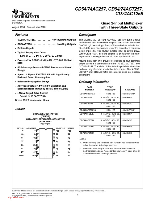
Data sheet acquired from Harris SemiconductorSCHS248AFeatures•’AC257, ’ACT257. . . . . . . . . . . . .Non-Inverting Outputs •CD74ACT258 . . . . . . . . . . . . . . . . . . .Inverting Outputs •Buffered Inputs•Typical Propagation Delay- 4.4ns at V CC = 5V , T A = 25o C, C L = 50pF•Exceeds 2kV ESD Protection MIL-STD-883, Method 3015•SCR-Latchup-Resistant CMOS Process and Circuit Design •Speed of Bipolar FAST™/AS/S with Significantly Reduced Power Consumption •Balanced Propagation Delays•AC Types Feature 1.5V to 5.5V Operation and Balanced Noise Immunity at 30% of the Supply •±24mA Output Drive Current -Fanout to 15 FAST™ ICs Drives 50Ω Transmission LinesPinoutCD54AC257, CD54ACT257(CERDIP)CD74AC257, CD74ACT257, CD74ACT258(PDIP , SOIC)TOP VIEWDescriptionThe ’AC257,’ACT257and CD74ACT258are quad 2-input multiplexers with three-state outputs that utilize Advanced CMOS Logic technology.Each of these devices selects four bits of data from two sources under the control of a common Select input (S).The Output Enable (OE)is active LOW.When OE is HIGH,all of the outputs (Y or Y)are in the high-impedance state regardless of all other input conditions.Moving data from two groups of registers to four common output buses is a common use of the ’AC257,’ACT257,and CD74ACT258.The state of the Select input determines the particular register from which the data comes.The ’AC257,’ACT257and CD74ACT258can also be used as function generators.14151691312111012345768S 1I 01I 11Y 2I 02I 1GND 2Y V CC 4I 04I 14Y 3I 03I 13YOE AC/ACT257ACT258ACT258AC/ACT257V CC 4I 04I 14Y 3I 03I 13YOE S1I 01I 11Y 2I 02I 1GND2Y Ordering InformationPART NUMBER TEMP.RANGE (o C)PACKAGE CD54AC257F3A -55 to 12516 Ld CERDIPCD74AC257E 0 to 70o C, -40 to 85,-55 to 12516 Ld PDIPCD74AC257M0 to 70o C, -40 to 85,-55 to 12516 Ld SOICCD54ACT257F3A -55 to 12516 Ld CERDIPCD74ACT257E 0 to 70o C, -40 to 85,-55 to 12516 Ld PDIPCD74ACT257M 0 to 70o C, -40 to 85,-55 to 12516 Ld SOICCD74ACT258E 0 to 70o C, -40 to 85,-55 to 12516 Ld PDIPCD74ACT258M 0 to 70o C, -40 to 85,-55 to 12516 Ld SOICNOTES:1.When ordering,use the entire part number.Add the suffix 96to obtain the variant in the tape and reel.2.Wafer and die for this part number is available which meets allelectrical specifications.Please contact your local TI sales office or customer service for ordering information.August 1998 - Revised May 2000CD54/74AC257, CD54/74ACT257,CD74ACT258Quad 2-Input Multiplexer with Three-State OutputsFunctional DiagramTRUTH TABLEOUTPUTENABLE SELECT INPUTDATA INPUTS 257OUTPUTS258OUTPUTSOE S I 0I 1Y Y H X X X Z Z L L L X L H L L H X H L L H X L L H LHXHHLH = High level voltage, L = Low level voltage, Z = High impedance (off) state, X = Don’t Care251114613103471294Y3Y2Y1Y1Y4Y3Y2YAC/ACT 257AC/ACT 2581I 02I 03I 04I 01I 12I 13I 14I 1S OE115Absolute Maximum Ratings Thermal InformationDC Supply Voltage, V CC. . . . . . . . . . . . . . . . . . . . . . . .-0.5V to 6V DC Input Diode Current, I IKFor V I < -0.5V or V I > V CC + 0.5V. . . . . . . . . . . . . . . . . . . . . .±20mA DC Output Diode Current, I OKFor V O < -0.5V or V O > V CC + 0.5V . . . . . . . . . . . . . . . . . . . .±50mA DC Output Source or Sink Current per Output Pin, I OFor V O > -0.5V or V O < V CC + 0.5V . . . . . . . . . . . . . . . . . . . .±50mA DC V CC or Ground Current, I CC or I GND (Note 3) . . . . . . . . .±100mA Operating ConditionsTemperature Range, T A . . . . . . . . . . . . . . . . . . . . . .-55o C to 125o C Supply Voltage Range, V CC (Note 4)AC T ypes. . . . . . . . . . . . . . . . . . . . . . . . . . . . . . . . . . .1.5V to 5.5V ACT T ypes . . . . . . . . . . . . . . . . . . . . . . . . . . . . . . . . .4.5V to 5.5V DC Input or Output Voltage, V I, V O . . . . . . . . . . . . . . . . .0V to V CC Input Rise and Fall Slew Rate, dt/dvAC T ypes, 1.5V to 3V . . . . . . . . . . . . . . . . . . . . . . . . .50ns (Max) AC T ypes, 3.6V to 5.5V. . . . . . . . . . . . . . . . . . . . . . . .20ns (Max) ACT T ypes, 4.5V to 5.5V. . . . . . . . . . . . . . . . . . . . . . .10ns (Max)Thermal Resistance (T ypical, Note 5)θJA (o C/W) PDIP Package. . . . . . . . . . . . . . . . . . . . . . . . . . . . .___ SOIC Package. . . . . . . . . . . . . . . . . . . . . . . . . . . . .___ Maximum Junction T emperature (Plastic Package) . . . . . . . . . .150o C Maximum Storage Temperature Range . . . . . . . . . .-65o C to 150o C Maximum Lead Temperature (Soldering 10s). . . . . . . . . . . . .300o CCAUTION:Stresses above those listed in“Absolute Maximum Ratings”may cause permanent damage to the device.This is a stress only rating and operation of the device at these or any other conditions above those indicated in the operational sections of this specification is not implied.NOTES:3.For up to 4 outputs per device, add±25mA for each additional output.4.Unless otherwise specified, all voltages are referenced to ground.5.θJA is measured with the component mounted on an evaluation PC board in free air.DC Electrical SpecificationsPARAMETER SYMBOLTESTCONDITIONSV CC(V)25o C-40o C TO85o C-55o C TO125o CUNITS V I(V)I O(mA)MIN MAX MIN MAX MIN MAXAC TYPESHigh Level Input Voltage V IH-- 1.5 1.2- 1.2- 1.2-V3 2.1- 2.1- 2.1-V5.5 3.85- 3.85- 3.85-V Low Level Input Voltage V IL-- 1.5-0.3-0.3-0.3V3-0.9-0.9-0.9V5.5- 1.65- 1.65- 1.65V High Level Output Voltage V OH V IH or V IL-0.05 1.5 1.4- 1.4- 1.4-V-0.053 2.9- 2.9- 2.9-V-0.05 4.5 4.4- 4.4- 4.4-V-43 2.58- 2.48- 2.4-V-24 4.5 3.94- 3.8- 3.7-V-75(Note 6, 7)5.5-- 3.85---V-50(Note 6, 7)5.5---- 3.85-VLow Level Output VoltageV OLV IH or V IL0.05 1.5-0.1-0.1-0.1V 0.053-0.1-0.1-0.1V 0.05 4.5-0.1-0.1-0.1V 123-0.36-0.44-0.5V 24 4.5-0.36-0.44-0.5V 75(Note 6, 7) 5.5--- 1.65--V 50(Note 6, 7)5.5----- 1.65V Input Leakage Current I I V CC or GND - 5.5-±0.1-±1-±1µA Three-State Leakage CurrentI OZV IH or V IL V O =V CC or GND - 5.5-±0.5-±5-±10µAQuiescent Supply Current MSI I CCV CC or GND0 5.5-8-80-160µAACT TYPESHigh Level Input Voltage V IH -- 4.5 to 5.52-2-2-V Low Level Input Voltage V IL -- 4.5 to 5.5-0.8-0.8-0.8V High Level Output VoltageV OHV IH or V IL-0.05 4.5 4.4- 4.4- 4.4-V -24 4.5 3.94- 3.8- 3.7-V -75(Note 6, 7) 5.5-- 3.85---V -50(Note 6, 7)5.5---- 3.85-V Low Level Output VoltageV OLV IH or V IL0.05 4.5-0.1-0.1-0.1V 24 4.5-0.36-0.44-0.5V 75(Note 6, 7) 5.5--- 1.65--V 50(Note 6, 7)5.5----- 1.65V Input Leakage Current I I V CC or GND - 5.5-±0.1-±1-±1µA Three-State or Leakage CurrentI OZV IH or V IL V O =V CC or GND - 5.5-±0.5-±5-±10µAQuiescent Supply Current MSII CC V CC or GND 0 5.5-8-80-160µA Additional Supply Current per Input Pin TTL Inputs High 1 Unit Load ∆I CCV CC -2.1-4.5 to5.5-2.4-2.8-3mANOTES:6.Test one output at a time for a 1-second maximum duration.Measurement is made by forcing current and measuring voltage to minimize power dissipation.7.Test verifies a minimum 50Ω transmission-line-drive capability at 85o C, 75Ω at 125o C.DC Electrical Specifications(Continued)PARAMETERSYMBOL TEST CONDITIONSV CC (V)25o C -40o C TO 85o C -55o C TO 125o C UNITS V I (V)I O (mA)MIN MAX MIN MAX MIN MAXACT Input Load TableINPUT UNIT LOADData0.83S 1.27OE 1.27NOTE:Unit load is∆I CC limit specified in DC Electrical SpecificationsT able, e.g., 2.4mA max at 25o C.Switching Specifications Input t r, t f = 3ns, C L= 50pF (Worst Case)PARAMETER SYMBOL V CC (V)-40o C TO 85o C-55o C TO 125o CUNITS MIN TYP MAX MIN TYP MAXAC TYPESPropagation Delay, In to YAC/ACT257t PLH, t PHL 1.5--106--117ns3.3(Note 9)3.3-11.8 3.3-13ns5(Note 10)2.4-8.5 2.3-9.3nsPropagation Delay, S to YAC/ACT257t PLH, t PHL 1.5--153--168ns3.34.8-17.1 4.7-18.8ns5 3.5-12.2 3.4-13.4nsPropagation Delay, OE to YAC/ACT257t PLZ, t PHZ,t PZL, t PZH1.5--167--184ns3.3 5.3-18.7 5.2-20.6ns5 3.8-13.4 3.7-14.7nsPropagation Delay, In to Y’AC/CD74ACT258t PLH, t PHL 1.5--91--100ns3.3 2.9-10.2 2.8-11.2ns5 2.1-7.32-8nsPropagation Delay, S to Y’AC/CD74ACT258t PLH, t PHL 1.5--153--168ns3.34.8-17.1 4.7-18.8ns5 3.5-12.2 3.4-13.4nsPropagation Delay, OE to Y’AC/CD74ACT258t PLZ, t PHZ,t PZL, t PZH1.5--167--184ns3.3 5.3-18.7 5.2-20.6ns5 3.8-13.4 3.7-14.7nsThree-State OutputCapacitanceC O---15--15pF Input Capacitance C I---10--10pFPower Dissipation Capacitance C PD(Note 11)--130--130-pF ACT TYPESPropagation Delay, In to YAC/ACT257t PLH, t PHL5(Note 10)2.8-9.7 2.7-10.7nsPropagation Delay,S to YAC/ACT257t PLH, t PHL54-14 3.9-15.4nsPropagation Delay,OE to Y AC/ACT257t PLZ , t PHZ ,t PZL , t PZH 54.1-14.64-16.1nsPropagation Delay,In to Y’AC/CD74ACT258t PLH , t PHL5 2.4-8.5 2.3-9.3nsPropagation Delay,S to Y’AC/CD74ACT258t PLH , t PHL54-14 3.9-15.4nsPropagation Delay,OE to Y’AC/CD74ACT258t PLZ , t PHZ ,t PZL , t PZH5 4.1-14.64-16.1nsThree-State Output Capacitance C O ---15--15pF Input CapacitanceC I ---10--10pF Power Dissipation Capacitance C PD (Note 11)--130--130-pFNOTES:8.Limits tested 100%.9.3.3V Min is at 3.6V, Max is at 3V.10.5V Min is at 5.5V, Max is at 4.5V.11.C PD is used to determine the dynamic power consumption per multiplexer.AC: P D = C PD V CC 2 f i +∑ (C L V CC 2 f o )ACT:P D =C PD V CC 2f i +∑(C L V CC 2f o )+V CC ∆I CC where f i =input frequency,f o =output frequency,C L =output load capacitance,V CC = supply voltage.FIGURE 1.THREE-STATE PROPAGATION DELAY TIMES AND TEST CIRCUITSwitching Specifications Input t r , t f = 3ns, C L = 50pF (Worst Case)(Continued)PARAMETERSYMBOL V CC (V)-40o C TO 85o C-55o C TO 125o CUNITS MIN TYP MAX MIN TYP MAX DUT WITH THREE-STATE OUTPUTINPUT LEVEL90%V S 10%GNDt f = 3nst PZLt PZHt PLZt PHZOUTPUTS ENABLEDOUTPUTS DISABLEDOUTPUT:LOW TO OFF TO LOWOUTPUT:HIGH TO OFF TO HIGHOTHER INPUTS (TIED HIGH OR LOW)OUTPUT DISABLEC L 50pF500Ω†R L 500Ω†R LOUT V S0.2V CCV OL (≠GND)V OH (≠V CC )0.8 V CC V SGND (t PHZ,t PZH )OUTPUTS ENABLEDOPEN (t PHL,t PLH )2 V CC (t PLZ,t PZL )(OPEN DRAIN)t r = 3ns OUTPUT DISABLE†FOR AC SERIES ONL Y: WHEN V CC = 1.5V , R L = 1k ΩFIGURE 2.INPUTS OR SELECT TO OUTPUT PROPAGATIONDELAYS (AC/ACT257)FIGURE 3.SELECT TO OUTPUT PROPAGATION DELAYS(CD74ACT258)90%10%t f = 3nst r = 3ns nI 0, nI 1, St PLHt PHLV SYINPUT LEVELGNDV S INPUT LEVEL V SSt PLHt PHLV SYDUT OUTPUTR L (NOTE)OUTPUT LOAD500ΩC L 50pFNOTE:For AC Series Only: When V CC = 1.5V , R L = 1k Ω.FIGURE 4.PROPAGATION DELAY TIMESACACT Input LevelV CC 3V Input Switching Voltage, V S 0.5 V CC 1.5V Output Switching Voltage, V S0.5 V CC0.5 V CCIMPORTANT NOTICETexas Instruments Incorporated and its subsidiaries (TI)reserve the right to make corrections,modifications,enhancements,improvements,and other changes to its products and services at any time and to discontinue any product or service without notice.Customers should obtain the latest relevant information before placing orders and should verify that such information is current and complete.All products are sold subject to TI’s terms and conditions of sale supplied at the time of order acknowledgment.TI warrants performance of its hardware products to the specifications applicable at the time of sale in accordance with TI’s standard warranty.Testing and other quality control techniques are used to the extent TI deems necessary to support this warranty.Except where mandated by government requirements,testing of all parameters of each product is not necessarily performed.TI assumes no liability for applications assistance or customer product design.Customers are responsible for their products and applications using TI components.To minimize the risks associated with customer products and applications,customers should provide adequate design and operating safeguards.TI does not warrant or represent that any license,either express or implied,is granted under any TI patent right,copyright,mask work right,or other TI intellectual property right relating to any combination,machine,or process in which TI products or services are rmation published by TI regarding third-party products or services does not constitute a license from TI to use such products or services or a warranty or endorsement e of such information may require a license from a third party under the patents or other intellectual property of the third party,or a license from TI under the patents or other intellectual property of TI.Reproduction of information in TI data books or data sheets is permissible only if reproduction is without alteration and isaccompanied by all associated warranties,conditions,limitations,and notices.Reproduction of this information with alteration is an unfair and deceptive business practice.TI is not responsible or liable for such altered documentation.Resale of TI products or services with statements different from or beyond the parameters stated by TI for that product or service voids all express and any implied warranties for the associated TI product or service and is an unfair and deceptive business practice.TI is not responsible or liable for any such statements.TI products are not authorized for use in safety-critical applications (such as life support)where a failure of the TI product would reasonably be expected to cause severe personal injury or death,unless officers of the parties have executed an agreementspecifically governing such use.Buyers represent that they have all necessary expertise in the safety and regulatory ramifications of their applications,and acknowledge and agree that they are solely responsible for all legal,regulatory and safety-related requirements concerning their products and any use of TI products in such safety-critical applications,notwithstanding any applications-related information or support that may be provided by TI.Further,Buyers must fully indemnify TI and its representatives against any damages arising out of the use of TI products in such safety-critical applications.TI products are neither designed nor intended for use in military/aerospace applications or environments unless the TI products are specifically designated by TI as military-grade or "enhanced plastic."Only products designated by TI as military-grade meet military specifications.Buyers acknowledge and agree that any such use of TI products which TI has not designated as military-grade is solely at the Buyer's risk,and that they are solely responsible for compliance with all legal and regulatory requirements in connection with such use.TI products are neither designed nor intended for use in automotive applications or environments unless the specific TI products are designated by TI as compliant with ISO/TS 16949requirements.Buyers acknowledge and agree that,if they use any non-designated products in automotive applications,TI will not be responsible for any failure to meet such requirements.Following are URLs where you can obtain information on other Texas Instruments products and application solutions:Products Applications AmplifiersAudioDataConvertersAutomotiveDSPBroadband Interface Digital Control Logic MilitaryPower Mgmt Optical Networking Microcontrollers Security Low Power Telephony WirelessVideo &Imaging WirelessMailing Address:Texas Instruments,Post Office Box 655303,Dallas,Texas 75265Copyright ©2007,Texas Instruments Incorporatedht t p ://oPACKAGING INFORMATIONOrderable Device Status(1)PackageType PackageDrawingPins PackageQtyEco Plan(2)Lead/Ball Finish MSL Peak Temp(3)CD54AC257F3A ACTIVE CDIP J161TBD A42N/A for Pkg Type CD54ACT257F3A ACTIVE CDIP J161TBD A42N/A for Pkg Type CD74AC257E ACTIVE PDIP N1625Pb-Free(RoHS)CU NIPDAU N/A for Pkg TypeCD74AC257EE4ACTIVE PDIP N1625Pb-Free(RoHS)CU NIPDAU N/A for Pkg TypeCD74AC257M ACTIVE SOIC D1640Green(RoHS&no Sb/Br)CU NIPDAU Level-1-260C-UNLIMCD74AC257M96ACTIVE SOIC D162500Green(RoHS&no Sb/Br)CU NIPDAU Level-1-260C-UNLIMCD74AC257M96E4ACTIVE SOIC D162500Green(RoHS&no Sb/Br)CU NIPDAU Level-1-260C-UNLIMCD74AC257M96G4ACTIVE SOIC D162500Green(RoHS&no Sb/Br)CU NIPDAU Level-1-260C-UNLIMCD74AC257ME4ACTIVE SOIC D1640Green(RoHS&no Sb/Br)CU NIPDAU Level-1-260C-UNLIMCD74AC257MG4ACTIVE SOIC D1640Green(RoHS&no Sb/Br)CU NIPDAU Level-1-260C-UNLIMCD74ACT257E ACTIVE PDIP N1625Pb-Free(RoHS)CU NIPDAU N/A for Pkg TypeCD74ACT257EE4ACTIVE PDIP N1625Pb-Free(RoHS)CU NIPDAU N/A for Pkg TypeCD74ACT257M ACTIVE SOIC D1640Green(RoHS&no Sb/Br)CU NIPDAU Level-1-260C-UNLIMCD74ACT257M96ACTIVE SOIC D162500Green(RoHS&no Sb/Br)CU NIPDAU Level-1-260C-UNLIMCD74ACT257M96E4ACTIVE SOIC D162500Green(RoHS&no Sb/Br)CU NIPDAU Level-1-260C-UNLIMCD74ACT257M96G4ACTIVE SOIC D162500Green(RoHS&no Sb/Br)CU NIPDAU Level-1-260C-UNLIMCD74ACT257ME4ACTIVE SOIC D1640Green(RoHS&no Sb/Br)CU NIPDAU Level-1-260C-UNLIMCD74ACT257MG4ACTIVE SOIC D1640Green(RoHS&no Sb/Br)CU NIPDAU Level-1-260C-UNLIMCD74ACT258M ACTIVE SOIC D1640Green(RoHS&no Sb/Br)CU NIPDAU Level-2-260C-1YEARCD74ACT258M96ACTIVE SOIC D162500Green(RoHS&no Sb/Br)CU NIPDAU Level-2-260C-1YEARCD74ACT258M96E4ACTIVE SOIC D162500Green(RoHS&no Sb/Br)CU NIPDAU Level-2-260C-1YEARCD74ACT258M96G4ACTIVE SOIC D162500Green(RoHS&no Sb/Br)CU NIPDAU Level-2-260C-1YEARCD74ACT258ME4ACTIVE SOIC D1640Green(RoHS&no Sb/Br)CU NIPDAU Level-2-260C-1YEARCD74ACT258MG4ACTIVE SOIC D1640Green(RoHS&no Sb/Br)CU NIPDAU Level-2-260C-1YEAR(1)The marketing status values are defined as follows:ACTIVE:Product device recommended for new designs.LIFEBUY:TI has announced that the device will be discontinued,and a lifetime-buy period is in effect.NRND:Not recommended for new designs.Device is in production to support existing customers,but TI does not recommend using this part in a new design.PREVIEW:Device has been announced but is not in production.Samples may or may not be available.OBSOLETE:TI has discontinued the production of the device.(2)Eco Plan-The planned eco-friendly classification:Pb-Free(RoHS),Pb-Free(RoHS Exempt),or Green(RoHS&no Sb/Br)-please check /productcontent for the latest availability information and additional product content details.TBD:The Pb-Free/Green conversion plan has not been defined.Pb-Free(RoHS):TI's terms"Lead-Free"or"Pb-Free"mean semiconductor products that are compatible with the current RoHS requirements for all6substances,including the requirement that lead not exceed0.1%by weight in homogeneous materials.Where designed to be soldered at high temperatures,TI Pb-Free products are suitable for use in specified lead-free processes.Pb-Free(RoHS Exempt):This component has a RoHS exemption for either1)lead-based flip-chip solder bumps used between the die and package,or2)lead-based die adhesive used between the die and leadframe.The component is otherwise considered Pb-Free(RoHS compatible)as defined above.Green(RoHS&no Sb/Br):TI defines"Green"to mean Pb-Free(RoHS compatible),and free of Bromine(Br)and Antimony(Sb)based flame retardants(Br or Sb do not exceed0.1%by weight in homogeneous material)(3)MSL,Peak Temp.--The Moisture Sensitivity Level rating according to the JEDEC industry standard classifications,and peak solder temperature.Important Information and Disclaimer:The information provided on this page represents TI's knowledge and belief as of the date that it is provided.TI bases its knowledge and belief on information provided by third parties,and makes no representation or warranty as to the accuracy of such information.Efforts are underway to better integrate information from third parties.TI has taken and continues to take reasonable steps to provide representative and accurate information but may not have conducted destructive testing or chemical analysis on incoming materials and chemicals.TI and TI suppliers consider certain information to be proprietary,and thus CAS numbers and other limited information may not be available for release.In no event shall TI's liability arising out of such information exceed the total purchase price of the TI part(s)at issue in this document sold by TI to Customer on an annual basis.分销商库存信息:TICD74ACT257M96G4CD74ACT258M96G4CD74ACT257MG4 CD74ACT258MG4。
SN74LVC573A中文资料

元器件交易网IMPORTANT NOTICETexas Instruments and its subsidiaries (TI) reserve the right to make changes to their products or to discontinueany product or service without notice, and advise customers to obtain the latest version of relevant informationto verify, before placing orders, that information being relied on is current and complete. All products are soldsubject to the terms and conditions of sale supplied at the time of order acknowledgement, including thosepertaining to warranty, patent infringement, and limitation of liability.TI warrants performance of its semiconductor products to the specifications applicable at the time of sale inaccordance with TI’s standard warranty. Testing and other quality control techniques are utilized to the extentTI deems necessary to support this warranty. Specific testing of all parameters of each device is not necessarilyperformed, except those mandated by government requirements.CERTAIN APPLICATIONS USING SEMICONDUCTOR PRODUCTS MAY INVOLVE POTENTIAL RISKS OFDEATH, PERSONAL INJURY, OR SEVERE PROPERTY OR ENVIRONMENTAL DAMAGE (“CRITICALAPPLICATIONS”). TI SEMICONDUCTOR PRODUCTS ARE NOT DESIGNED, AUTHORIZED, ORWARRANTED TO BE SUITABLE FOR USE IN LIFE-SUPPORT DEVICES OR SYSTEMS OR OTHERCRITICAL APPLICATIONS. INCLUSION OF TI PRODUCTS IN SUCH APPLICATIONS IS UNDERSTOOD TOBE FULLY AT THE CUSTOMER’S RISK.In order to minimize risks associated with the customer’s applications, adequate design and operatingsafeguards must be provided by the customer to minimize inherent or procedural hazards.TI assumes no liability for applications assistance or customer product design. TI does not warrant or representthat any license, either express or implied, is granted under any patent right, copyright, mask work right, or otherintellectual property right of TI covering or relating to any combination, machine, or process in which suchsemiconductor products or services might be or are used. TI’s publication of information regarding any thirdparty’s products or services does not constitute TI’s approval, warranty or endorsement thereof.Copyright © 1998, Texas Instruments Incorporated。
hc573完整中文资料
74hc573中文资料参数-74hc573引脚图-功能原理-74hC573的作用-应用电路-74hC563-54hC57高性能硅门 CMOS器件SL74HC573跟 LS/AL573的管脚一样。
器件的输入是和标准CMOS输出兼容的;加上拉电阻,他们能和 LS/ALSTTL输出兼容。
当锁存使能端为高时,这些器件的锁存对于数据是透明的(也就是说输出同步)。
当锁存使能变低时,符合建立时间和保持时间的数据会被锁存。
×输出能直接接到CMOS,NMOS和 TTL接口上×操作电压范围:~×低输入电流:×CMOS器件的高噪声抵抗特性·三态总线驱动输出·置数全并行存取·缓冲控制输入·使能输入有改善抗扰度的滞后作用原理说明:M54HC563/74HC563/M54HC573/74HC573的八个锁存器都是透明的D 型锁存器,当使能(G)为高时,Q 输出将随数据(D)输入而变。
当使能为低时,输出将锁存在已建立的数据电平上。
输出控制不影响锁存器的内部工作,即老数据可以保持,甚至当输出被关闭时,新的数据也可以置入。
这种电路可以驱动大电容或低阻抗负载,可以直接与系统总线接口并驱动总线,而不需要外接口。
特别适用于缓冲寄存器,I/O 通道,双向总线驱动器和工作寄存器。
HC563引脚功能表:HC573引脚功能表:12,13,14,15,16,17,18,19Q0 to Q7 3 State Latch Outputs 3态锁存输出11LE Latch Enable Input 锁存使能输入10GND Ground接地(0V)20VCC Positive Supply Voltage电源电压图1 HC573引脚图图2 HC573 国际电工委员会逻辑符号图3 HC563引脚图图4 HC563 国际电工委员会逻辑符号图5 HC563 逻辑图图6HC573 逻辑图图7 输入输出等效电路真值表:INPUTS 输入Outputs输出OE LE D Q (HC573) Q (HC563)H X X Z ZL L X NO CHANGE *NO CHANGE * L H L L HL H H H LABSOLUTE MAXIMUM RATINGS绝对最大额定值:TopOperating Temperature: M54HC Series M74HC Series操作温度: M54HC 系列M74HC系列-55 to +125 -40 to +85℃tr,tf Input Rise and Fall Time输入上升和下降时间VCC = 2V0 to 1000ns VCC =0 to 500VCC = 6V0 to 400VOHHigh Level Output Voltage输出高电平电压VI = VIH or VILIO=-20 μ 4.54.44 Level Output Voltage输出低电平电压VI = VIH or VILIO=20μ Leakage Current输入漏电流 =VCC or GND--±±1±1μAIOZState Output Off State Current关断状态3态输出电流 =VIH or VIL VO =VCC or GND--±±±10μAICCQuiescent Supply Current静态电源电流 =VCC or GND--4-40-80μA应用电路图:点击图片查看大图图8。
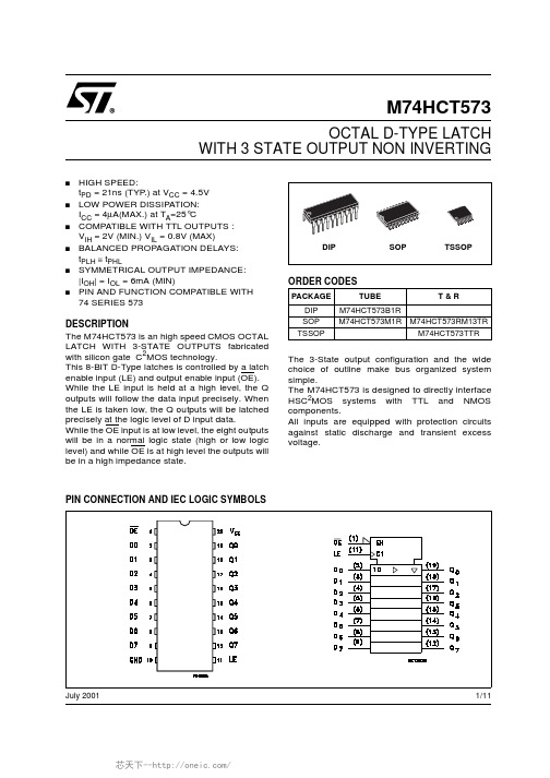
CD74ACT573中文资料

Data sheet acquired from Harris SemiconductorSCHS291This data sheet is applicable to the CD74AC563, CD54/74AC573, and CD54/74ACT573. The CD54AC563 and CD54/74ACT563 werenot acquired from Harris Semiconductor.IMPORTANT NOTICETexas Instruments and its subsidiaries (TI) reserve the right to make changes to their products or to discontinue any product or service without notice, and advise customers to obtain the latest version of relevant information to verify, before placing orders, that information being relied on is current and complete. All products are sold subject to the terms and conditions of sale supplied at the time of order acknowledgement, including those pertaining to warranty, patent infringement, and limitation of liability.TI warrants performance of its semiconductor products to the specifications applicable at the time of sale in accordance with TI’s standard warranty. Testing and other quality control techniques are utilized to the extent TI deems necessary to support this warranty. Specific testing of all parameters of each device is not necessarily performed, except those mandated by government requirements.CERTAIN APPLICATIONS USING SEMICONDUCTOR PRODUCTS MAY INVOLVE POTENTIAL RISKS OF DEATH, PERSONAL INJURY, OR SEVERE PROPERTY OR ENVIRONMENTAL DAMAGE (“CRITICAL APPLICATIONS”). TI SEMICONDUCTOR PRODUCTS ARE NOT DESIGNED, AUTHORIZED, OR WARRANTED TO BE SUITABLE FOR USE IN LIFE-SUPPORT DEVICES OR SYSTEMS OR OTHER CRITICAL APPLICATIONS. INCLUSION OF TI PRODUCTS IN SUCH APPLICATIONS IS UNDERSTOOD TO BE FULLY AT THE CUSTOMER’S RISK.In order to minimize risks associated with the customer’s applications, adequate design and operating safeguards must be provided by the customer to minimize inherent or procedural hazards.TI assumes no liability for applications assistance or customer product design. TI does not warrant or represent that any license, either express or implied, is granted under any patent right, copyright, mask work right, or other intellectual property right of TI covering or relating to any combination, machine, or process in which such semiconductor products or services might be or are used. TI’s publication of information regarding any third party’s products or services does not constitute TI’s approval, warranty or endorsement thereof.Copyright © 1999, Texas Instruments Incorporated。
DM74AS573N中文资料

© 2000 Fairchild Semiconductor Corporation DS006313October 1986Revised March 2000DM74AS573 Octal D-Type Transparent Latch with 3-STATE OutputsDM74AS573Octal D-Type Transparent Latch with 3-STATE OutputsGeneral DescriptionThese 8-bit registers feature totem-pole 3-STATE outputs designed specifically for driving highly-capacitive or rela-tively low-impedance loads. The high-impedance state and increased HIGH-logic-level drive provide these registers with the capability of being connected directly to and driv-ing the bus lines in a bus-organized system without need for interface or pull-up components. They are particularly attractive for implementing buffer registers, I/O ports, bidi-rectional bus drivers, and working registers.The eight latches of the DM74AS573 are transparent D-type latches, meaning that while the enable (G) is HIGH the Q outputs will follow the data (D) inputs. When the enable is taken LOW the output will be latched at the level of the data that was set UP .A buffered output control input can be used to place the eight outputs in either a normal logic state (HIGH or LOW logic levels) or a high-impedance state. In the high-imped-ance state the outputs neither load nor drive the bus lines significantly.The output control does not affect the internal operation of the latches. That is, the old data can be retained or new data can be entered even while the outputs are OFF.The pin-out is arranged to ease printed circuit board layout.All data inputs are on one side of the package while all the outputs are on the other side.Featuress Switching specifications at 50 pFs Switching specifications guaranteed over full tempera-ture and V CC range s Advanced oxide-isolated, ion-implanted Schottky TTL process s Functionally equivalent with DM74S373s Improved AC performance over DM74S373 at approxi-mately half the power s 3-STATE buffer-type outputs drive bus lines directly s Bus structured pinoutOrdering Code:Devices also available in T ape and Reel. Specify by appending the suffix letter “X” to the ordering code.Connection DiagramOrder Number Package NumberPackage DescriptionDM74AS573WM M20B 20-Lead Small Outline Integrated Circuit (SOIC), JEDEC MS-013, 0.300 Wide DM74AS573NN20A20-Lead Plastic Dual-In-Line Package (PDIP), JEDEC MS-001, 0.300 Wide 2D M 74A S 573Function TableL = LOW State H = HIGH State X = Don’t CareZ = High Impedance State Q 0 = Previous Condition of QLogic DiagramOutput EnableOutputControlG D Q L H H H L H L L L L X Q 0HXXZDM74AS573Absolute Maximum Ratings (Note 1)Note 1: The “Absolute Maximum Ratings” are those values beyond which the safety of the device cannot be guaranteed. The device should not be operated at these limits. The parametric values defined in the Electrical Characteristics tables are not guaranteed at the absolute maximum ratings.The “Recommended Operating Conditions” table will define the conditions for actual device operation.Recommended Operating ConditionsNote 2: The (↑) arrow indicates the positive edge of the Clock is used for reference.Electrical Characteristicsover recommended operating free air temperature range. All typical values are measured at V CC = 5V, T A = 25°C.Note 3: The output conditions have been chosen to produce a current that approximates one half of the true short-circuit output current, I OS .Supply Voltage 7V Input Voltage7V Voltage Applied to Disabled Output 5.5VOperating Free Air Temperature Range 0°C to +70°C Storage Temperature Range −65°C to +150°CTypical θJA N Package 52.0°C/W M Package70.0°C/WSymbol ParameterMin Nom Max Units V CC Supply Voltage4.555.5V V IH HIGH Level Input Voltage 2V V IL LOW Level Input Voltage 0.8V I OH HIGH Level Output Current −15mA I OL LOW Level Output Current 48mA t W Width of Enable Pulse HIGH 4.5ns LOW5.5t SU Data Setup Time (Note 2)2↑ns t H Data Hold Time (Note 2)3↑ns T AFree Air Operating Temperature70°CSymbol ParameterConditionsMinTypMax Units V IK Input Clamp Voltage V CC = 4.5V, I I = −18 mA−1.2V V OH HIGH Level V CC = 4.5V, V IL = Max, I OH = Max 2.4 3.3V Output Voltage V CC = 4.5V to 5.5V, I OH = −2 mA V CC − 2V OL LOW Level V CC = 4.5V, V IH = 2V 0.350.5V Output VoltageI OL = MaxI I Input Current @ Max Input Voltage V CC = 5.5V, V IH = 7V0.1mA I IH HIGH Level Input Current V CC = 5.5V, V IH = 2.7V 20µA I ILLOW Level Input Current V CC = 5.5V, V IL = 0.4V −0.5mA I O (Note 3)Output Drive Current V CC = 5.5V, V O = 2.25V −30−112mA I OZH OFF-State Output Current,V CC = 5.5V, V IH = 2V,50µA HIGH Level Voltage Applied V O = 2.7VI OZL Off-State Output Current,V CC = 5.5V, V IH = 2V,−50µALow Level Voltage Applied V O = 0.4V I CCSupply CurrentV CC = 5.5V Outputs HIGH 5693Outputs OpenOutputs LOW 5590mAOutputs Disabled65106 4D M 74A S 573Switching Characteristicsover recommended operating free air temperature range Symbol ParameterConditionsFrom To Min Max Units t PLH Propagation Delay Time V CC = 4.5V to 5.5V Data Any Q 36ns LOW-to-HIGH Level Output R L = 500Ωt PHL Propagation Delay Time C L = 50 pFData Any Q 36ns HIGH-to-LOW Level Output t PLH Propagation Delay Time Enable Any Q 611.5ns LOW-to-HIGH Level Output t PHL Propagation Delay Time Enable Any Q 47.5ns HIGH-to-LOW Level Output t PZH Output Enable Time Output Control Any Q 2 6.5 ns to HIGH Level Output t PZL Output Enable Time Output Control Any Q 49.5ns to LOW Level Output t PHZ Output Disable Time Output Control Any Q 2 6.5ns from HIGH Level Output t PLZOutput Disable Time Output ControlAny Q27nsfrom LOW Level Output DM74AS573Physical Dimensions inches (millimeters) unless otherwise noted20-Lead Small Outline Integrated Circuit (SOIC), JEDEC MS-013, 0.300 WidePackage Number M20B6D M 74A S 573 O c t a l D -T y p e T r a n s p a r e n t L a t c h w i t h 3-S T A TE O u t p u t sPhysical Dimensions inches (millimeters) unless otherwise noted (Continued)20-Lead Plastic Dual-In-Line Package (PDIP), JEDEC MS-001, 0.300 WidePackage Number N20AFairchild does not assume any responsibility for use of any circuitry described, no circuit patent licenses are implied and Fairchild reserves the right at any time without notice to change said circuitry and specifications.LIFE SUPPORT POLICYFAIRCHILD’S PRODUCTS ARE NOT AUTHORIZED FOR USE AS CRITICAL COMPONENTS IN LIFE SUPPORT DEVICES OR SYSTEMS WITHOUT THE EXPRESS WRITTEN APPROVAL OF THE PRESIDENT OF FAIRCHILD SEMICONDUCTOR CORPORATION. As used herein:1.Life support devices or systems are devices or systems which, (a) are intended for surgical implant into the body, or (b) support or sustain life, and (c) whose failure to perform when properly used in accordance with instructions for use provided in the labeling, can be rea-sonably expected to result in a significant injury to the user. 2. A critical component in any component of a life support device or system whose failure to perform can be rea-sonably expected to cause the failure of the life support device or system, or to affect its safety or effectiveness.。
TEXAS INSTRUMENTS CD74AC00, CD74ACT00 说明书

Data sheet acquired from Harris Semiconductor SCHS223Features•Typical Propagation Delay- 3.2ns at V CC = 5V , T A = 25o C, C L = 50pF•Exceeds 2kV ESD Protection MIL-STD-883, Method 3015•SCR-Latchup-Resistant CMOS Process and Circuit Design•Speed of Bipolar FAST™/AS/S with Significantly Reduced Power Consumption •Balanced Propagation Delays•AC Types Feature 1.5V to 5.5V Operation and Balanced Noise Immunity at 30% of the Supply •±24mA Output Drive Current -Fanout to 15 FAST™ ICs-Drives 50Ω Transmission LinesDescriptionThe CD74AC00and CD74ACT00are quad 2-input NAND gates that utilize the Harris Advanced CMOS Logic technology.PinoutCD74AC00, CD74ACT00(PDIP , SOIC)TOP VIEWFunctional DiagramOrdering InformationPART NUMBER TEMP.RANGE (o C)PACKAGE PKG.NO.CD74AC00E -55 to 12514 Ld PDIP E14.3CD74ACT00E -55 to 12514 Ld PDIP E14.3CD74AC00M -55 to 12514 Ld SOIC M14.15CD74ACT00M -55 to 12514 Ld SOICM14.15NOTES:1.When ordering,use the entire part number.Add the suffix 96to obtain the variant in the tape and reel.2.Wafer and die for this part number is available which meets all elec-trical specifications.Please contact your local sales office or Harris customer service for ordering information.1A 1B 1Y 2A 2B 2Y GND V CC 4A 4B 4Y 3A 3B 3Y1234567141312111098TRUTH TABLEINPUTSOUTPUTSA B Y L L H H L H L H H HHL1A 1B 2A 2B 3B 3A 4B 4A12459101213368111Y 2Y3Y 4YGND = 7V CC = 14September 1998CAUTION: These devices are sensitive to electrostatic discharge. Users should follow proper IC Handling Procedures.CD74AC00,CD74ACT00Quad 2-Input NAND GateFile Number1855.1查询CD74AC00供应商Absolute Maximum Ratings Thermal InformationDC Supply Voltage, V CC. . . . . . . . . . . . . . . . . . . . . . . .-0.5V to 6V DC Input Diode Current, I IKFor V I < -0.5V or V I > V CC + 0.5V. . . . . . . . . . . . . . . . . . . . . .±20mA DC Output Diode Current, I OKFor V O < -0.5V or V O > V CC + 0.5V . . . . . . . . . . . . . . . . . . . .±50mA DC Output Source or Sink Current per Output Pin, I OFor V O > -0.5V or V O < V CC + 0.5V . . . . . . . . . . . . . . . . . . . .±50mA DC V CC or Ground Current, I CC or I GND (Note 3) . . . . . . . . .±100mA Operating ConditionsTemperature Range, T A . . . . . . . . . . . . . . . . . . . . . .-55o C to 125o C Supply Voltage Range, V CC (Note 4)AC T ypes. . . . . . . . . . . . . . . . . . . . . . . . . . . . . . . . . . .1.5V to 5.5V ACT T ypes . . . . . . . . . . . . . . . . . . . . . . . . . . . . . . . . .4.5V to 5.5V DC Input or Output Voltage, V I, V O . . . . . . . . . . . . . . . . .0V to V CC Input Rise and Fall Slew Rate, dt/dvAC T ypes, 1.5V to 3V . . . . . . . . . . . . . . . . . . . . . . . . .50ns (Max) AC T ypes, 3.6V to 5.5V. . . . . . . . . . . . . . . . . . . . . . . .20ns (Max) ACT T ypes, 4.5V to 5.5V. . . . . . . . . . . . . . . . . . . . . . .10ns (Max)Thermal Resistance (T ypical, Note 5)θJA (o C/W) PDIP Package. . . . . . . . . . . . . . . . . . . . . . . . . . . . .90 SOIC Package. . . . . . . . . . . . . . . . . . . . . . . . . . . . .175 Maximum Junction T emperature (Plastic Package) . . . . . . . . . .150o C Maximum Storage Temperature Range . . . . . . . . . .-65o C to 150o C Maximum Lead Temperature (Soldering 10s). . . . . . . . . . . . .300o CCAUTION:Stresses above those listed in“Absolute Maximum Ratings”may cause permanent damage to the device.This is a stress only rating and operation of the device at these or any other conditions above those indicated in the operational sections of this specification is not implied.NOTES:3.For up to 4 outputs per device, add±25mA for each additional output.4.Unless otherwise specified, all voltages are referenced to ground.5.θJA is measured with the component mounted on an evaluation PC board in free air.DC Electrical SpecificationsPARAMETER SYMBOLTESTCONDITIONS VCC(V)25o C-40o C TO85o C-55o C TO125o CUNITS V I(V)I O(mA)MIN MAX MIN MAX MIN MAXAC TYPESHigh Level Input Voltage V IH-- 1.5 1.2- 1.2- 1.2-V3 2.1- 2.1- 2.1-V5.5 3.85- 3.85- 3.85-V Low Level Input Voltage V IL-- 1.5-0.3-0.3-0.3V3-0.9-0.9-0.9V5.5- 1.65- 1.65- 1.65V High Level Output Voltage V OH V IH or V IL-0.05 1.5 1.4- 1.4- 1.4-V-0.053 2.9- 2.9- 2.9-V-0.05 4.5 4.4- 4.4- 4.4-V-43 2.58- 2.48- 2.4-V-24 4.5 3.94- 3.8- 3.7-V-75(Note 6, 7)5.5-- 3.85---V-50(Note 6, 7)5.5---- 3.85-VLow Level Output VoltageV OLV IH or V IL0.05 1.5-0.1-0.1-0.1V 0.053-0.1-0.1-0.1V 0.05 4.5-0.1-0.1-0.1V 123-0.36-0.44-0.5V 24 4.5-0.36-0.44-0.5V 75(Note 6, 7) 5.5--- 1.65--V 50(Note 6, 7)5.5----- 1.65V Input Leakage Current I I V CC or GND - 5.5-±0.1-±1-±1µA Quiescent Supply Current,SSI I CCV CC or GND5.5-4-40-80µAACT TYPESHigh Level Input Voltage V IH -- 4.5 to 5.52-2-2-V Low Level Input Voltage V IL -- 4.5 to 5.5-0.8-0.8-0.8V High Level Output VoltageV OHV IH or V IL-0.05 4.5 4.4- 4.4- 4.4-V -24 4.5 3.94- 3.8- 3.7-V -75 5.5-- 3.85---V -505.5---- 3.85-V Low Level Output VoltageV OLV IH or V IL0.05 4.5-0.1-0.1-0.1V 24 4.5-0.36-0.44-0.5V 75(Note 6, 7) 5.5--- 1.65--V 50(Note 6, 7)5.5----- 1.65V Input Leakage Current I I V CC or GND - 5.5-±0.1-±1-±1µA Quiescent Supply Current,SSII CC V CC or GND 0 5.5-4-40-80µA Additional Supply Current per Input Pin TTL Inputs High 1 Unit Load ∆I CCV CC -2.1- 4.5 to 5.5- 2.4- 2.8-3mANOTES:6.Test one output at a time for a 1-second maximum duration.Measurement is made by forcing current and measuring voltage to minimize power dissipation.7.Test verifies a minimum 50Ω transmission-line-drive capability at 85o C, 75Ω at 125o C.ACT Input Load TableINPUT UNIT LOADAll0.15NOTE:Unit load is ∆I CC limit specified in DC Electrical Specifications T able, e.g., 2.4mA max at 25o C.DC Electrical Specifications(Continued)PARAMETERSYMBOL TEST CONDITIONSV CC (V)25o C -40o C TO 85o C -55o C TO 125o C UNITS V I (V)I O (mA)MIN MAX MIN MAX MIN MAXSwitching Specifications Input t r , t f = 3ns, C L = 50pF (Worst Case)PARAMETERSYMBOLV CC (V)-40o C TO 85o C-55o C TO 125o CUNITSMIN TYPMAXMINTYPMAXAC TYPESPropagation Delay, Input to Outputt PLH , t PHL1.5--83--91ns 3.3(Note 9)2.7-9.3 2.6-10.2ns 5(Note 10)1.9- 6.6 1.8-7.3ns Input CapacitanceC I ---10--10pF Power Dissipation Capacitance C PD (Note 11)--45--45-pFACT TYPESPropagation Delay, Input to Outputt PHL 5(Note 10)2.8-8 2.7-8ns t PLH3.4-9.5 3.3-9.5ns Input CapacitanceC I ---10--10pF Power Dissipation Capacitance C PD (Note 11)--45--45-pFNOTES:8.Limits tested at 100%.9.3.3V Min at 3.6V, Max at 3V.10.5V Min at 5.5V, Max at 4.5V.11.C PD is used to determine the dynamic power consumption per gate.AC: P D = V CC 2 f i (C PD + C L )ACT: P D = V CC 2 f i (C PD + C L ) + V CC ∆I CC where f i = input frequency, C L = output load capacitance, V CC = supply voltage.DUT OUTPUTR L (NOTE)OUTPUT LOAD500ΩC L 50pFNOTE:For AC Series Only: When V CC = 1.5V , R L = 1k Ω.FIGURE 1.PROPAGATION DELAY TIMESCD74ACCD74ACTInput LevelV CC 3V Input Switching Voltage, V S 0.5 V CC 1.5V Output Switching Voltage, V S0.5 V CC0.5 V CCFIGURE 2.WAVEFORMSt r = 3ns t f = 3ns90%V S 10%GNDINPUT t PHLt PLHV SLEVEL V I V OIMPORTANT NOTICETexas Instruments and its subsidiaries (TI) reserve the right to make changes to their products or to discontinue any product or service without notice, and advise customers to obtain the latest version of relevant information to verify, before placing orders, that information being relied on is current and complete. All products are sold subject to the terms and conditions of sale supplied at the time of order acknowledgement, including those pertaining to warranty, patent infringement, and limitation of liability.TI warrants performance of its semiconductor products to the specifications applicable at the time of sale in accordance with TI’s standard warranty. Testing and other quality control techniques are utilized to the extent TI deems necessary to support this warranty. Specific testing of all parameters of each device is not necessarily performed, except those mandated by government requirements.CERTAIN APPLICATIONS USING SEMICONDUCTOR PRODUCTS MAY INVOLVE POTENTIAL RISKS OF DEATH, PERSONAL INJURY, OR SEVERE PROPERTY OR ENVIRONMENTAL DAMAGE (“CRITICAL APPLICATIONS”). TI SEMICONDUCTOR PRODUCTS ARE NOT DESIGNED, AUTHORIZED, OR WARRANTED TO BE SUITABLE FOR USE IN LIFE-SUPPORT DEVICES OR SYSTEMS OR OTHER CRITICAL APPLICATIONS. INCLUSION OF TI PRODUCTS IN SUCH APPLICATIONS IS UNDERSTOOD TO BE FULLY AT THE CUSTOMER’S RISK.In order to minimize risks associated with the customer’s applications, adequate design and operating safeguards must be provided by the customer to minimize inherent or procedural hazards.TI assumes no liability for applications assistance or customer product design. TI does not warrant or represent that any license, either express or implied, is granted under any patent right, copyright, mask work right, or other intellectual property right of TI covering or relating to any combination, machine, or process in which such semiconductor products or services might be or are used. TI’s publication of information regarding any third party’s products or services does not constitute TI’s approval, warranty or endorsement thereof.Copyright © 1999, Texas Instruments Incorporated。
M74HCT573TTR,M74HCT573TTR,M74HCT573TTR,M74HCT573B1R,M74HCT573RM13TR, 规格书,Datasheet 资料
1/11July 2001sHIGH SPEED:t PD = 21ns (TYP .) at V CC = 4.5V sLOW POWER DISSIPATION:I CC = 4µA(MAX.) at T A =25°CsCOMPATIBLE WITH TTL OUTPUTS : V IH = 2V (MIN.) V IL = 0.8V (MAX)sBALANCED PROPAGATION DELAYS:t PLH ≅ t PHLsSYMMETRICAL OUTPUT IMPEDANCE:|I OH | = I OL = 6mA (MIN)sPIN AND FUNCTION COMPATIBLE WITH 74 SERIES 573DESCRIPTIONThe M74HCT573 is an high speed CMOS OCTAL LATCH WITH 3-STATE OUTPUTS fabricated with silicon gate C 2MOS technology.This 8-BIT D-Type latches is controlled by a latch enable input (LE) and output enable input (OE).While the LE input is held at a high level, the Q outputs will follow the data input precisely. When the LE is taken low, the Q outputs will be latched precisely at the logic level of D input data.While the OE input is at low level, the eight outputs will be in a normal logic state (high or low logic level) and while OE is at high level the outputs will be in a high impedance state.The 3-State output configuration and the wide choice of outline make bus organized system simple.The M74HCT573 is designed to directly interface HSC 2MOS systems with TTL and NMOS components.All inputs are equipped with protection circuits against static discharge and transient excess voltage.M74HCT573OCTAL D-TYPE LATCHWITH 3 STATE OUTPUT NON INVERTINGPIN CONNECTION AND IEC LOGIC SYMBOLSORDER CODESPACKAGE TUBE T & RDIP M74HCT573B1R SOP M74HCT573M1RM74HCT573RM13TR TSSOPM74HCT573TTRM74HCT5732/11INPUT AND OUTPUT EQUIVALENT CIRCUITPIN DESCRIPTIONTRUTH TABLEX: Don’t CareZ: High Impedance(*): Q Outputs are latched at the time when the LE input is taken low logic level.LOGIC DIAGRAMPIN No SYMBOL NAME AND FUNCTION 1OE 3 State Output Enable Input (Active LOW)2, 3, 4, 5, 6, 7, 8, 9D0 to D7Data Inputs12, 13, 14, 15, 16, 17, 18, 19Q0 to Q73 State Latch Outputs11LE Latch Enable Input 10GND Ground (0V)20V CCPositive Supply VoltageINPUTSOUTPUTSOE LE D QH X X ZL L X NO CHANGE (*)L H L L LHHHM74HCT5733/11ABSOLUTE MAXIMUM RATINGSAbsolute Maximum Ratings are those values beyond which damage to the device may occur. Functional operation under these conditions is not implied(*) 500mW at 65 °C; derate to 300mW by 10mW/°C from 65°C to 85°CRECOMMENDED OPERATING CONDITIONSSymbol ParameterValue Unit V CC Supply Voltage -0.5 to +7V V I DC Input Voltage -0.5 to V CC + 0.5V V O DC Output Voltage -0.5 to V CC + 0.5V I IK DC Input Diode Current ± 20mA I OK DC Output Diode Current ± 20mA I O DC Output Current ± 35mA I CC or I GND DC V CC or Ground Current± 70mA P D Power Dissipation 500(*)mW T stg Storage Temperature -65 to +150°C T LLead Temperature (10 sec)300°CSymbol ParameterValue Unit V CC Supply Voltage 4.5 to 5.5V V I Input Voltage 0 to V CC V V O Output Voltage 0 to V CC V T op Operating Temperature-55 to 125°C t r , t fInput Rise and Fall Time (V CC = 4.5 to 5.5V)0 to 500nsM74HCT5734/11DC SPECIFICATIONSAC ELECTRICAL CHARACTERISTICS (C L = 50 pF, Input t r = t f = 6ns)SymbolParameterTest ConditionValue UnitV CC (V)T A = 25°C -40 to 85°C -55 to 125°C Min.Typ.Max.Min.Max.Min.Max.V IHHigh Level Input Voltage4.5 to5.5 2.02.02.0V V IL Low Level Input Voltage4.5 to5.50.80.80.8V V OH High Level Output Voltage4.5I O =-20 µA 4.4 4.5 4.4 4.4VI O =-6.0 mA 4.184.31 4.134.10V OL Low Level Output Voltage4.5I O =20 µA 0.00.10.10.1V I O =6.0 mA 0.170.260.330.40I I Input Leakage Current5.5V I = V CC or GND ± 0.1± 1± 1µA I OZ High Impedance Output Leakage Current5.5V I = V IH or V IL V O = V CC or GND ± 0.5± 5± 10µA I CC Quiescent Supply Current5.5V I = V CC or GND 44080µA ∆ I CCAdditional Worst Case Supply Current5.5Per Input pin V I = 0.5V or V I = 2.4V Other Inputs at V CC or GND2.02.93.0mASymbolParameterTest ConditionValue UnitV CC (V)C L (pF)T A = 25°C -40 to 85°C -55 to 125°C Min.Typ.Max.Min.Max.Min.Max.t TLH t THL Output TransitionTime4.5507121518ns t PLH t PHL Propagation DelayTime (LE - Q,Q) 4.55021334150ns 4.515025394959t PLH t PHL Propagation DelayTime (D - Q,Q) 4.55019303845ns 4.515023364554t PZL t PZH Output EnableTime 4.550R L = 1 K Ω19303845ns 4.515023364554t PLZ t PHZ Output DisableTime4.550R L = 1 K Ω18253138ns t W(L) t W(H)Minimum PulseWidth (LE) 4.5507151922ns t s Minimum Set-Up Time4.5504101315ns t hMinimum Hold Time4.550555nsM74HCT5735/11CAPACITIVE CHARACTERISTICS1) C PD is defined as the value of the IC’s internal equivalent capacitance which is calculated from the operating current consumption without load. (Refer to Test Circuit). Average operating current can be obtained by the following equation. I CC(opr) = C PD x V CC x f IN + I CC /8 (per Flip Flop)TEST CIRCUITC L = 50pF/150pF or equivalent (includes jig and probe capacitance)R 1 = 1K Ω or equivalentR T = Z OUT of pulse generator (typically 50Ω)SymbolParameterTest ConditionValue UnitV CC (V)T A = 25°C -40 to 85°C -55 to 125°C Min.Typ.Max.Min.Max.Min.Max.C IN Input Capacitance5101010pF C OUT OutputCapacitance10pF C PDPower Dissipation Capacitance (note 1)51pF TESTSWITCH t PLH , t PHL Open t PZL , t PLZ V CC t PZH , t PHZGNDM74HCT5736/11WAVEFORM 1: LE TO Qn PROPAGATION DELAYS, LE MINIMUM PULSE WIDTH, Dn TO LE SETUP AND HOLD TIMES(f=1MHz; 50% duty cycle)M74HCT5737/11WAVEFORM 2: OUTPUT ENABLE AND DISABLE TIMES (f=1MHz; 50% duty cycle)WAVEFORM 3: PROPAGATION DELAY TIMES(f=1MHz; 50% duty cycle)M74HCT573 Information furnished is believed to be accurate and reliable. However, STMicroelectronics assumes no responsibility for the consequences of use of such information nor for any infringement of patents or other rights of third parties which may result from its use. No license is granted by implication or otherwise under any patent or patent rights of STMicroelectronics. Specifications mentioned in this publication are subject to change without notice. This publication supersedes and replaces all information previously supplied. STMicroelectronics products are not authorized for use as critical components in life support devices or systems without express written approval of STMicroelectronics.© The ST logo is a registered trademark of STMicroelectronics© 2000 STMicroelectronics - Printed in Italy - All Rights ReservedSTMicroelectronics GROUP OF COMPANIESAustralia - Brazil - China - Finland - France - Germany - Hong Kong - India - Italy - Japan - Malaysia - Malta - MoroccoSingapore - Spain - Sweden - Switzerland - United Kingdom© 11/11芯天下--/。
- 1、下载文档前请自行甄别文档内容的完整性,平台不提供额外的编辑、内容补充、找答案等附加服务。
- 2、"仅部分预览"的文档,不可在线预览部分如存在完整性等问题,可反馈申请退款(可完整预览的文档不适用该条件!)。
- 3、如文档侵犯您的权益,请联系客服反馈,我们会尽快为您处理(人工客服工作时间:9:00-18:30)。
Data sheet acquired from Harris SemiconductorSCHS291This data sheet is applicable to the CD74AC563, CD54/74AC573, and CD54/74ACT573. The CD54AC563 and CD54/74ACT563 werenot acquired from Harris Semiconductor.PACKAGING INFORMATIONOrderable Device Status(1)PackageType PackageDrawingPins PackageQtyEco Plan(2)Lead/Ball Finish MSL Peak Temp(3)CD54AC573F3A ACTIVE CDIP J201TBD A42SNPB N/A for Pkg Type CD54ACT573F3A ACTIVE CDIP J201TBD A42SNPB N/A for Pkg Type CD74AC563E ACTIVE PDIP N2020Pb-Free(RoHS)CU NIPDAU N/A for Pkg TypeCD74AC563EE4ACTIVE PDIP N2020Pb-Free(RoHS)CU NIPDAU N/A for Pkg TypeCD74AC573E ACTIVE PDIP N2020Pb-Free(RoHS)CU NIPDAU N/A for Pkg TypeCD74AC573EE4ACTIVE PDIP N2020Pb-Free(RoHS)CU NIPDAU N/A for Pkg TypeCD74AC573M ACTIVE SOIC DW2025Green(RoHS&no Sb/Br)CU NIPDAU Level-1-260C-UNLIMCD74AC573M96ACTIVE SOIC DW202000Green(RoHS&no Sb/Br)CU NIPDAU Level-1-260C-UNLIMCD74AC573M96E4ACTIVE SOIC DW202000Green(RoHS&no Sb/Br)CU NIPDAU Level-1-260C-UNLIMCD74AC573M96G4ACTIVE SOIC DW202000Green(RoHS&no Sb/Br)CU NIPDAU Level-1-260C-UNLIMCD74AC573ME4ACTIVE SOIC DW2025Green(RoHS&no Sb/Br)CU NIPDAU Level-1-260C-UNLIMCD74AC573MG4ACTIVE SOIC DW2025Green(RoHS&no Sb/Br)CU NIPDAU Level-1-260C-UNLIMCD74ACT573E ACTIVE PDIP N2020Pb-Free(RoHS)CU NIPDAU N/A for Pkg TypeCD74ACT573EE4ACTIVE PDIP N2020Pb-Free(RoHS)CU NIPDAU N/A for Pkg TypeCD74ACT573M ACTIVE SOIC DW2025Green(RoHS&no Sb/Br)CU NIPDAU Level-1-260C-UNLIMCD74ACT573M96ACTIVE SOIC DW202000Green(RoHS&no Sb/Br)CU NIPDAU Level-1-260C-UNLIMCD74ACT573M96E4ACTIVE SOIC DW202000Green(RoHS&no Sb/Br)CU NIPDAU Level-1-260C-UNLIMCD74ACT573M96G4ACTIVE SOIC DW202000Green(RoHS&no Sb/Br)CU NIPDAU Level-1-260C-UNLIMCD74ACT573ME4ACTIVE SOIC DW2025Green(RoHS&no Sb/Br)CU NIPDAU Level-1-260C-UNLIMCD74ACT573MG4ACTIVE SOIC DW2025Green(RoHS&no Sb/Br)CU NIPDAU Level-1-260C-UNLIM(1)The marketing status values are defined as follows:ACTIVE:Product device recommended for new designs.LIFEBUY:TI has announced that the device will be discontinued,and a lifetime-buy period is in effect.NRND:Not recommended for new designs.Device is in production to support existing customers,but TI does not recommend using this part in a new design.PREVIEW:Device has been announced but is not in production.Samples may or may not be available.OBSOLETE:TI has discontinued the production of the device.(2)Eco Plan-The planned eco-friendly classification:Pb-Free(RoHS),Pb-Free(RoHS Exempt),or Green(RoHS&no Sb/Br)-please check /productcontent for the latest availability information and additional product content details.TBD:The Pb-Free/Green conversion plan has not been defined.Pb-Free(RoHS):TI's terms"Lead-Free"or"Pb-Free"mean semiconductor products that are compatible with the current RoHS requirementsfor all6substances,including the requirement that lead not exceed0.1%by weight in homogeneous materials.Where designed to be soldered at high temperatures,TI Pb-Free products are suitable for use in specified lead-free processes.Pb-Free(RoHS Exempt):This component has a RoHS exemption for either1)lead-based flip-chip solder bumps used between the die and package,or2)lead-based die adhesive used between the die and leadframe.The component is otherwise considered Pb-Free(RoHS compatible)as defined above.Green(RoHS&no Sb/Br):TI defines"Green"to mean Pb-Free(RoHS compatible),and free of Bromine(Br)and Antimony(Sb)based flame retardants(Br or Sb do not exceed0.1%by weight in homogeneous material)(3)MSL,Peak Temp.--The Moisture Sensitivity Level rating according to the JEDEC industry standard classifications,and peak solder temperature.Important Information and Disclaimer:The information provided on this page represents TI's knowledge and belief as of the date that it is provided.TI bases its knowledge and belief on information provided by third parties,and makes no representation or warranty as to the accuracy of such information.Efforts are underway to better integrate information from third parties.TI has taken and continues to take reasonable steps to provide representative and accurate information but may not have conducted destructive testing or chemical analysis on incoming materials and chemicals.TI and TI suppliers consider certain information to be proprietary,and thus CAS numbers and other limited information may not be available for release.In no event shall TI's liability arising out of such information exceed the total purchase price of the TI part(s)at issue in this document sold by TI to Customer on an annual basis.TAPE AND REELINFORMATION*All dimensionsare nominalDevicePackage Type Package Drawing Pins SPQReel Diameter (mm)Reel Width W1(mm)A0(mm)B0(mm)K0(mm)P1(mm)W (mm)Pin1Quadrant CD74AC573M96SOIC DW 202000330.024.410.813.0 2.712.024.0Q1CD74ACT573M96SOICDW202000330.024.410.813.02.712.024.0Q1PACKAGE MATERIALS INFORMATION11-Mar-2008*Alldimensions are nominalDevice Package TypePackage DrawingPins SPQ Length (mm)Width (mm)Height (mm)CD74AC573M96SOIC DW 202000346.0346.041.0CD74ACT573M96SOICDW202000346.0346.041.0PACKAGE MATERIALS INFORMATION11-Mar-2008Pack Materials-Page 2IMPORTANT NOTICETexas Instruments Incorporated and its subsidiaries(TI)reserve the right to make corrections,modifications,enhancements,improvements, and other changes to its products and services at any time and to discontinue any product or service without notice.Customers should obtain the latest relevant information before placing orders and should verify that such information is current and complete.All products are sold subject to TI’s terms and conditions of sale supplied at the time of order acknowledgment.TI warrants performance of its hardware products to the specifications applicable at the time of sale in accordance with TI’s standard warranty.Testing and other quality control techniques are used to the extent TI deems necessary to support this warranty.Except where mandated by government requirements,testing of all parameters of each product is not necessarily performed.TI assumes no liability for applications assistance or customer product design.Customers are responsible for their products and applications using TI components.To minimize the risks associated with customer products and applications,customers should provide adequate design and operating safeguards.TI does not warrant or represent that any license,either express or implied,is granted under any TI patent right,copyright,mask work right, or other TI intellectual property right relating to any combination,machine,or process in which TI products or services are rmation published by TI regarding third-party products or services does not constitute a license from TI to use such products or services or a warranty or endorsement e of such information may require a license from a third party under the patents or other intellectual property of the third party,or a license from TI under the patents or other intellectual property of TI.Reproduction of TI information in TI data books or data sheets is permissible only if reproduction is without alteration and is accompanied by all associated warranties,conditions,limitations,and notices.Reproduction of this information with alteration is an unfair and deceptive business practice.TI is not responsible or liable for such altered rmation of third parties may be subject to additional restrictions.Resale of TI products or services with statements different from or beyond the parameters stated by TI for that product or service voids all express and any implied warranties for the associated TI product or service and is an unfair and deceptive business practice.TI is not responsible or liable for any such statements.TI products are not authorized for use in safety-critical applications(such as life support)where a failure of the TI product would reasonably be expected to cause severe personal injury or death,unless officers of the parties have executed an agreement specifically governing such use.Buyers represent that they have all necessary expertise in the safety and regulatory ramifications of their applications,and acknowledge and agree that they are solely responsible for all legal,regulatory and safety-related requirements concerning their products and any use of TI products in such safety-critical applications,notwithstanding any applications-related information or support that may be provided by TI.Further,Buyers must fully indemnify TI and its representatives against any damages arising out of the use of TI products in such safety-critical applications.TI products are neither designed nor intended for use in military/aerospace applications or environments unless the TI products are specifically designated by TI as military-grade or"enhanced plastic."Only products designated by TI as military-grade meet military specifications.Buyers acknowledge and agree that any such use of TI products which TI has not designated as military-grade is solely at the Buyer's risk,and that they are solely responsible for compliance with all legal and regulatory requirements in connection with such use. TI products are neither designed nor intended for use in automotive applications or environments unless the specific TI products are designated by TI as compliant with ISO/TS16949requirements.Buyers acknowledge and agree that,if they use any non-designated products in automotive applications,TI will not be responsible for any failure to meet such requirements.Following are URLs where you can obtain information on other Texas Instruments products and application solutions:Products ApplicationsAmplifiers AudioData Converters AutomotiveDSP BroadbandClocks and Timers Digital ControlInterface MedicalLogic MilitaryPower Mgmt Optical NetworkingMicrocontrollers SecurityRFID TelephonyRF/IF and ZigBee®Solutions Video&ImagingWirelessMailing Address:Texas Instruments,Post Office Box655303,Dallas,Texas75265Copyright©2008,Texas Instruments Incorporated。