A Practical Guide for X-Ray Diffraction Characterization of Ga(Al, In)N Alloys
西大催化剂表征X射线衍射

(1) 这样,通过实验测定衍射方向θ,就可以通过(1)式计 算立方晶系的晶胞参数a。
23
七、电子的散射强度和原子的散射因子
晶体对x 射线的衍射强度是由晶 体一个晶胞中原子的种类、数目和 排列方式决定的,整个晶体在各方 向的衍射强度,实际上是一个晶胞 衍射强度的若干倍。 图1.5 中O 点处的电子在x 射线 照射下将发生散射,可以证明,散 射x 射线在P 点的强度可用下式表 示:
(2)
|F(hkl)|被称作结构振幅。又由于衍射强度与晶胞 中原子的分布有关,即与晶体的结构有关,F(hkl)被
叫作结构因子。经过复杂的推导,可以得出如下公式:
|F(hkl)|2=[Σfj cos2π(hxj+kyj+lzj)]2+ [Σfj sin2π (hxj+kyj+lzj)]2 (3)
26
式中(hkl)是衍射指标,(xj, yj, zj)是原子的分数坐标,即 代表原子在晶胞中的位臵。 (3)式是计算晶胞在各衍射方向衍射x 射线的相对强度的 重要公式。该公式把衍射的相对强度与晶胞中原子的位臵 联系起来,通过对衍射强度的测定,则可得到晶胞中原子 分布的信息。 利用(3)式测定晶体结构的具体做法是:首先假设一可 能的结构,由该结构对应晶胞中原子的分数坐标(xj, yj, zj) 推算出不同衍射指标(hkl)所代表的各衍射方向的|F(hkl)|2 值,即相对强度。然后将实验结果与推算结果进行比较, 若一致说明假设的结构为晶体的真实结构;若不一致, 再重新假设一个结构并推算和比较,直至所假设结构的 衍射峰相对强度与实际XRD 谱图的衍射峰相对强度一致 为止。
13
晶面可用晶面指标(h*k*l*)标记, 其定义为晶面在三个晶轴上的 倒易截数的互质整数之比。 对于图 1.2 的晶面,其在 三个晶轴上的截数分别为 3,
xrd衍射及应用

X射线衍射的方法及应用从1912年,马克思·冯·劳埃发现晶格中晶面的距离与X射线相近,晶体材料可以作为X射线天然的三维光栅以来。
X射线衍射逐渐发展成为了一种有效的高科技无损检测技术来分析许许多多的材料,包括流体、矿物、聚合物、药物、薄膜材料、陶瓷、半导体等等。
X射线衍射可以提供直观的材料的结构信息,如相、织构和平均晶粒尺寸、缺陷、结晶度等结构参数。
X-Ray Diffraction: Instrumentation and Applications(ANDREI A. BUNACIU; ELENA GABRIELA UDRI¸STIOIU; HASSAN Y. ABOUL-ENEIN. Critical Reviews in Analytical Chemistry.2015,45,289-299)这篇文章首先简单介绍了关于X射线衍射的基础理论,之后着重介绍了X射线衍射仪的原理构造、样品制备以及XRD技术在制药生产、法医学、地质学、微电子工业、玻璃制造以及腐蚀分析六个领域的应用。
Micro-XRD study of beta–titanium wires and infrared soldered joints(Masahiro Iijimaa,∗, William A. Brantleyb, Naoki Babac, Satish B. Alapatid,Toshihiro Yuasaa, Hiroki Ohnoe, Itaru Mizoguchia。
Dental Materials.2007,23,1051–1056)针对红外焊接的beta-Ti丝接头做了微区X射线衍射分析。
X-Ray Diffraction: Instrumentation and Applications(ANDREI A. BUNACIU; ELENA GABRIELA UDRI¸STIOIU; HASSAN Y. ABOUL-ENEIN. Critical Reviews in Analytical Chemistry.2015,45,289-299)中基础理论部分包括布拉格方程、X射线的发生以及测角仪的原理和光学布置等等,文章大致阐述了一下XRD的原理,这些与我们在课本上学到的基本一致。
衍射的应用 英语作文

Diffraction: A Fascinating Phenomenon in Our LivesDiffraction, a captivating phenomenon in physics, occurs when waves, such as light or sound, bend around obstacles. It is not merely a scientific curiosity but a fundamental process that shapes our daily experiences and technological advancements. In this essay, we will explore the fascinating applications of diffraction in various aspects of our lives.In Optics and ImagingOne of the most prominent applications of diffraction lies in optics and imaging. Microscopes and telescopes, instruments that have revolutionized our understanding of the microscopic and cosmic worlds, rely heavily on diffraction principles. While diffraction limits the resolution of these instruments by preventing the formation of infinitely small light spots, understanding and mitigating its effects have led to the development of advanced imaging techniques. For instance, diffraction gratings, optical elements with regularly spaced grooves, diffract light into distinct directions, enabling precise spectral analysis and high-resolution imaging in fields like astronomy and material science.In CommunicationsIn the realm of communications, diffraction plays a crucial role, particularly in fiber optics and wireless networking. In fiber optic cables, light signals propagate through thin glass fibers, experiencing diffraction as they interact with the fiber's boundaries. Engineers leverage this phenomenon to design efficient fiber couplers and splitters, ensuring seamless transmission of data over long distances. Moreover, in wireless networks, diffraction allows radio waves to bypass obstacles like buildings, ensuring reliable signal coverage even in urban environments with complex terrain.In Everyday ExperiencesDiffraction is not just confined to laboratories and high-tech equipment; it is a ubiquitous part of our daily lives. Have you ever noticed the rainbow-colored spots on a CD when illuminated by light? This mesmerizing display is a direct result of diffraction, as the tiny grooves on the CD surface scatter light waves in various directions. Similarly, the way sound waves diffract around corners and create echoes in large rooms is a testament to the pervasiveness of this phenomenon.In Art and DesignArtists and designers have also embraced diffraction to create unique and captivating visual effects. By manipulating light sources and obstacles, they can create intricate patterns and illusions that play with our perception of space and form. Theselight-based installations and performances often incorporate diffraction gratings or similar structures to achieve their stunning visual impacts.In Scientific ResearchIn the field of scientific research, diffraction is a powerful tool for probing the structure and properties of matter. For instance, X-ray diffraction has revolutionized our understanding of crystalline structures, enabling scientists to determine the atomic arrangements within solids. Similarly, electron diffraction in electron microscopes allows for imaging at atomic scales, pushing the boundaries of what we can see and know about the world around us.ConclusionIn conclusion, diffraction is a fascinating phenomenon that permeates every aspect of our lives, from the microscopic world of atoms to the vast expanse of the cosmos. Its applications range from advanced imaging techniques and communication systems to everyday experiences and artistic expressions. As we continue to explore and harness the power of diffraction, we can expect even more groundbreaking discoveries and innovations in the years to come.。
X-ray diffractometer
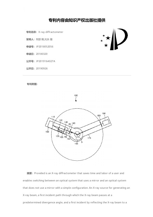
专利名称:X-ray diffractometer发明人:刑部 剛,光永 徹申请号:JP2018052056申请日:20180320公开号:JP2019164027A公开日:20190926专利内容由知识产权出版社提供专利附图:摘要:Provided is an X-ray diffractometer that saves time and labor of a user and enables switching between an optical system that uses a mirror and an optical system that does not use a mirror with a simple configuration. An X-ray source for generating an X-ray beam, a first incident path through which the X-ray beam passes at apredetermined divergence angle, and a first incident by reflecting the X-ray beam to amultilayer mirror. A second incident path that passes in parallel with the X-ray beam that has passed through the path, and the X-ray source 110, the first incident path, and the second incident path are moved in a predetermined direction while maintaining their relative positions. A moving mechanism; an incident slit 160 that allows an X-ray beam incident on the sample to pass through; and a sample support base 165 that supports the sample S at a position fixed with respect to the incident slit 160. Among the X-ray beams R1 and R2 that have passed through the second incident path or the second incident path, the X-ray beam that passes through the incident slit 160 is switched. [Selection] Figure 1申请人:株式会社リガク地址:東京都昭島市松原町3丁目9番12号国籍:JP代理人:福地 武雄,白川 洋一更多信息请下载全文后查看。
上海光源同步辐射技术讲习班

10月15日,第 天 一一学员报到与注册 (上海光源综合办公楼 楼大厅)
10月16日,第二天 线站介绍与衍射方法理论
9:00-9:30
讲习班开幕式及领导讲话
9:30-10:30
上海光源及衍射线站介绍 一高兴宇
10:30-11:00
茶歇,合影
18:00-19:00
晚餐
10月17日,第二天 衍射方法及其应用(1)
9:00-10:30
x-ray diffractio n and its applicatio n—麦振洪
10:30-11:00
茶歇11:00-1Fra bibliotek:30X射线掠入射散射技术及应用 一姜晓明
12:30-13:30
午餐
13:30-14:30
SSRF线站参观操作讲解及交流一杨铁莹
16:30-17:30
学员与讲师自由交流讨论
17:30-18:00
闭幕总结
18:00-19:00
晚餐
19:30-24:00
薄膜晶体结构分析(实习机时,大约8小时)
-----薄膜晶体点阵参数实地测量和点阵类型的测定, 杨平
粉末衍射法测定晶体结构实例讲解 吴国涛
14:30-15:30
X射线驻波场在薄膜表征中的应用 一李文斌
15:30-16:00
茶歇
16:00-17:00
冋步辐射在有机光电材料中的应用 一
张吉东
17:00-18:00
XRD技术在无序体系结构研究中的应用
—王晓东
18:00-19:00
晚餐
10月18日,第四天 衍射方法及其应用(2)
9:00-10:00
北化复试资料XRD分析
X-rayxrd 即X-ray diffraction 的缩写,X射线衍射,通过对材料进行X射线衍射,分析其衍射图谱,获得材料的成分、材料内部原子或分子的结构或形态等信息的研究手段。
布喇格定律X射线介绍X射线是一种波长很短(约为20~0.06┱)的电磁波,能穿透一定厚度的物质,并能使荧光物质发光、照相乳胶感光、气体电离。
在用电子束轰击金属“靶”产生的X射线中,包含与靶中各种元素对应的具有特定波长的X射线,称为特征(或标识)X射线。
定律由来考虑到X射线的波长和晶体内部原子间的距离(0.3-几nm)相近,1912年德国物理学家劳厄(M.von Laue)提出一个重要的科学预见:晶体可以作为X射线的空间衍射光栅,即当一束 X射线通过晶体时将发生衍射,衍射波叠加的结果使射线的强度在某些方向上加强,在其他方向上减弱。
分析在照相底片上得到的衍射花样,便可确定晶体结构。
这一预见随即为实验所验证。
1913年英国物理学家布喇格父子(W.H.Bragg,W.L.Bragg)在劳厄发现的基础上,不仅成功地测定了NaCl、KCl等的晶体结构,并提出了作为晶体衍射基础的著名公式──布喇格定律:2d sinθ=nλ式中λ为X射线的波长,n为任何正整数,又称衍射级数。
其上限为以下条件来表示:nmax=2dh0k0l0/λ,dh0k0l0<λ/2只有那些间距大于波长一半的面族才可能给出衍射,以此求纳米粒子的形貌。
满足定律的条件当X射线以掠角θ(入射角的余角)入射到某一点阵平面间距为d的原子面上时,在符合上式的条件下,将在反射方向上得到因叠加而加强的衍射线。
布喇格定律简洁直观地表达了衍射所必须满足的条件。
当 X射线波长λ已知时(选用固定波长的特征X射线),采用细粉末或细粒多晶体的线状样品,可从一堆任意取向的晶体中,从每一θ角符合布喇格条件的反射面得到反射,测出θ后,利用布喇格公式即可确定点阵平面间距、晶胞大小和类型;根据衍射线的强度,还可进一步确定晶胞内原子的排布。
x射线衍射成像技术最新发展详解

课程论文题目X射线衍射成像技术的原理以及最新发展与应用学院专业班级学生学号二〇年月日摘要随着科技的发展,基于傅里叶光学的X射线衍射技术发展越来越先进,形成了X射线衍射成像(X—ray diffraction imaging,XDI)和相干X射线衍射成像(coherent X-ray diffractive imaging,CXDI/CDI)等技术,它们广泛应用于材料、医学、生物、物理等领域,为人们探索微观世界的结构提供很好的工具。
本文主要论述了X射线衍射的基本原理,并讲述了它们在不同应用中的最新发展,包括X射线衍射成像和相干X射线衍射成像的二维、三维成像等技术,同时简单的说明了它们在一些领域的应用。
关键词:X射线衍射;X射线衍射成像;相干X射线衍射成像1前言近几十年来,X射线衍射成像技术得到快速发展,它具有不损伤样品、无污染、快捷、测量精度高、能得到有关晶体完整性的大量信息等优点,大量的用于材料内部结构分析、生物分子探究、医学以及危险品扫描等领域.近一个世纪以来,科学家们不断探索测定物质结构的方法,希望能够看到物质内部的原子是如何排列的。
而传统用的最多的方法是X射线晶体衍射分析的方法(XRD)能够实现物质的结构的测定,但它存在一定的局限性,然而在实际应用中,会受到很多的限制,为了更好的研究物质的结构,科学家们做了大量的工作,对X射线衍射技术进行改进升级,取得了一些最新的更成果,例如X射线衍射成像技术(X- ray diffraction imaging,XDI)、相干X射线衍射成像技术(coherent X—ray diffractive imaging,CXDI/CDI)等。
近年来,X射线衍射增强成像(X Ray Diffraction enhanced imaging,DEI)也发展迅速。
射线相位衬度成像是一种新型的X射线成像技术,通过记录射线穿过物体后相位的改变对物体进行成像,可以提供比传统的X射线吸收成像更高的图像衬度以及空间分辨力。
XRD

根据Benson Hart小角相机设计的小角散射附件 使广角衍射仪可以实现纳米材料的粒度测定,速 度快重现性好。
多功能粉晶X射线衍射仪(XRD)
1. 新型陶瓷X光管,光学预校 准设计,可提供点焦斑和线焦 斑,可自由切换 2. DOPS直接光学定位测角仪, 无磨损,抗振动,永远保持角 度精度0.0001度 3. 测角仪可进行theta-theta 或 theta-2theta扫描 4. 各种类型的探测器包括:正 比计数器、闪烁计数器、固体 探测器、超能探测器、PSD位 敏探测器等。其中超能探测器 属阵列探测器,其探测效率比 传统的正比或闪烁高100倍。
Journal of Polymer Science: Part A: Polymer Chemistry, Vol. 42, 853–861 (2004)
Chem. Eur. J. 2004, 10, 4954 – 4959
XRD patterns of 2 and 5 at a) room temperature and b) 150 ℃. The inset in b) shows the SAXS curve of 5 at 150 ℃.
在小分子领域,还是在大分子领域,多晶X射线衍 射所分析和测定的内容基本上是相同的。高聚物在 结构形态上有其自身的复杂性和特殊性,因此,用 X射线衍射考察高聚物时,必须结合具体情况进行
分析,以获得对真实情况恰当、准确的理解。
目前,在实际中,多晶照相法的大部分工 作已被多晶衍射仪法取代。 下面要介绍的四种应用均基于衍射仪法。 依次是: 物相分析; 结晶度测定; 取向测定; 晶粒尺寸测定
c. 盖革—弥勒(Ceiger-Muller)计数器 在SAXS中计数器用于测定弱的X射线。
- 1、下载文档前请自行甄别文档内容的完整性,平台不提供额外的编辑、内容补充、找答案等附加服务。
- 2、"仅部分预览"的文档,不可在线预览部分如存在完整性等问题,可反馈申请退款(可完整预览的文档不适用该条件!)。
- 3、如文档侵犯您的权益,请联系客服反馈,我们会尽快为您处理(人工客服工作时间:9:00-18:30)。
R ev i e wCo p yA practical guide for X-ray diffraction characterization of Ga(Al, In)N alloysS.Q. Zhou ),M. F. Wu and S. D. Yao )School of Physics, Peking University, Beijing, 100871, P. R. China AbstractGa(In, Al)N alloys are used as active layer or cladding layer in light emitting diodes and laser diodes. X-ray diffraction is extensively used to evaluate the crystalline quality, the chemical composition and the residual strain in Ga(Al, In)N thin film, which directly determine the emission wavelength and the device performance. Due to the minor mismatch in lattice parameter between the Ga(Al, In)N alloy and the GaN virtual substrate, X-ray diffraction comes to a problem to separate the signal from Ga(Al, In)N alloy and GaN. In this paper, we give a detailed comparison on different diffraction planes. Generally, in order to balance the intensity and peak separation between Ga(Al, In)N alloy and GaN, (0004) and (1015) planes make the best choice for symmetric scan, and asymmetric scan, respectively.PACS: ; 61.66.Fn; 68.55.NqKeywords: X-ray diffraction; Compound semiconductors; Thin films1. Introduction Driven by the commercialization of short wavelength light emitting diodes and laser diodes, the III–nitrides, aluminium nitride (AlN), gallium nitride (GaN) and indium nitride (InN), attract huge research attention [1]. They can form a continuous alloyE-mail address: zhousq2000@E-mail address: sdyao@R ev i e wCo p ysystem (InGaN, InAlN, AlGaN, or AlInGaN) whose direct optical bandgaps range from ~0.8 eV for InN [2] and 3.4 eV for GaN to 6.2 eV for AlN. For most LED and LD devices, a thin InGaN layer or InGaN multiple quantum wells work as the active layer, while a thin AlGaN layer works as the cladding or barrier layer [3, 4]. AlInGaN quaternary alloys allow an independent control of the lattice mismatch and band offset in AlInGaN-based heterostructures [5]. The structural quality, the In/Al composition in these thin layers directly determine the emission wavelength and the performance of the device. Therefore a precise determination of the composition and the interface quality is crucial to optimize the growth procedure and the properties of the alloys. High resolution X-ray diffraction is the well-known technique to characterize the crystalline structure by measuring the lattice parameters and their spreading, consequently the composition in the compounds can be deduced [6, 7]. Usually, in the fabrication of GaN-based LED, an intermediate buffer layer of GaN (1-2 um) is grown, to act as a buffer layer and to improve crystalline quality. The InGaN or AlGaN ternary alloys are then grown onto GaN layers. Thisconfiguration arises a crucial difficulty in X-ray diffraction measurement. As shown in Fig. 1, the lattice parameter for III-Nitrides are rather close to each other [8], which results in the alloy has a even more similar lattice parameter to GaN. The minor difference in lattice parameter and the same wurtzite structure together result in thedifficulty to separate the signal from Ga(Al, In)N alloys and GaN layers. In the typical X-ray diffraction spectrum, Ga(Al, In)N alloy expresses itself as a weak shoulder beside the strong peak of GaN, or even is completely overlapped by the GaN peak. In order to extract reliable information from the spectrum, it is strongly hoped that the peak of interesting layer is more separated from GaN peak, at the same time, with more intensity. In this paper, we carefully compared different diffraction planes,R ev i e wCo p yand gave a practical guide in X-ray diffraction measurement on Ga(Al, In)N/GaN heterostructures.2. ExperimentsThe x-ray measurements were performed using high resolution x-ray diffractometer equipped with a four-crystal monochromator in Ge(220) configuration and one or two 200 µm slits before the detector. The x-ray wavelength is 1.5406 Å. The sample is mounted on a four-circle (K ,2L ,M ,N )geonomitor. K and 2L are the incident angle and diffraction angle. O is defined as the angle between the sample surface and the horizontal plane, which is defined by the incident and diffraction lines. The angle N measures the rotation around the surface normal of the substrate. In skew symmetric diffraction geometry, the sample is tilted about the angle of the lattice plane inclination respect to the sample surface. The Ga(Al, In)N samples were grown on Al 2O 3(0001) by metal-organic chemical vapor deposition method. From X-ray diffraction and Rutherford backscattering/channeling measurements, all samples have very good quality.3. Results and discussionsThe basic principle of X-ray diffraction is Bragg’s Law. n d =sin 2,where d is thelattice spacing, is the Bragg angle and R is the incident X-ray wavelength. Therefore, in X-ray diffraction, the real measurement is on the variation of the lattice spacing. For symmetric (~h and k=0) Bragg reflections, only variations in lattice constant perpendicular to the sample surface can be detected. However, in the asymmetric case (measurement on the planes not parallel to the sample surface), both perpendicular and parallel lattice parameters contribute to the lattice spacing.R ev i e wCo p yWe investigated the symmetric case of (0002), (0004), and (0006) diffraction, and the asymmetric case of (101l ), with l =1 to 5, with the aim to collect the optimal spectrum. The optimal spectrum is supposed to possess three factors: (a) large angle separation between Ga(Al, In)N alloy and GaN, (b) small full width at half maximum (FWHM) and (c) strong diffraction intensity. In the following text, we give a practical guide to select the so-called optimal spectrum.3.1 Symmetric scanFor symmetric scan, K /2L scans of (0002), (0004) and (0006) planes were studied. The intensity, the FWHMs and the peak separation are shown in Fig. 2(a) and (b). Diffraction of (0002) planes has the strongest intensity, but the smallest peak separation, while diffraction of (0006) has the biggest peak separation. Depending on In/Al content in Ga(Al, In)N alloys, (0004) planes normally make the best balance between intensity and resolution. Fig. 3 shows K /2L scans of (0002) and (0004) for an AlInGaN layer on GaN. The pattern of (0004) allows more reliable determination on the lattice parameter in the AlInGaN layer.3.2 Asymmetric scanThe skew symmetric mode is used to do the asymmetric scan. K /2L scans of (1011),(1012), (1013), (1014) and (1015) planes were compared in Fig. 4. The diffraction of (1015) has the smallest FWHM (full width at half maximum), very strong intensity and biggest peak separation. Diffractions of (1011) and (1013) have strongestintensities, but have much bigger FWHMs, what’s more, the peak separation is smaller than that of (1015). So (1015) planes make the best choice for in-plane lattice constant determination. Fig. 5 compares the K /2L scans of an AlInGaN layerR ev i e wCo p yand obviously proves the optimal spectrum of (1015).4. ConclusionIn a conclusion, in X-ray diffraction measurement on Ga(Al, In)N alloys, the diffraction of (0004) gives a better balance between intensity and resolution depending on the composition variation of the alloys. In asymmetric case, the diffraction of (1015) definitely makes the best choice to get the strong intensity and best resolution. This rule can also be applied to the X-ray diffraction characterization of ion-implanted and MeV ion bombarded crystalline thin film. In that case, the damaged layer has a slight elongation in the perpendicular direction [10], which comes to a similar problem of InGaN alloys on GaN.AcknowledgementThe authors thank Dr. Liu Jianping for providing GaN samples. This work was supported by the Key Laboratory of Heavy Ion Physics, Ministry of Education, China, and by the National Natural Science Foundation of China under grant NO. 10375004.Reference[1] S. Nakamura and G. Fasol, The Blue Laser Diode-GaN Based Light Emitter and Lasers (Springer, Berlin, 1997).[2] K.M. Yu, Z. Liliental-Weber, W. Walukiewicz, W. Shan, J.W. Ager lll, S.X. Li, R.E. Jones, E.E. Haller,H. Lu, and W.J. Schaff, Appl. Phys. Lett. 86,071910-1 (2005). [3] S. Nakamura, T. Mukai, and M. Senoh, Appl. Phys. Lett. 64,1687, (1994) [4] S. Nakamura Semicond. Sci. Technol. 14 (1999) R27–R40.R ev i e wCo p y[5] M. Asif Khan, J.W. Yang, G. Simin, R. Gaska, M.S. Shur,H.-C. zur Loye, G. Tamulaitis, A. Zukauskas, Appl. Phys. Lett. 76 (2000) 1161.[6] M. Schuster, P.O. Gervais, B. Jobst, W. Hösler, R. Averbeck, H. Riechert, A. Iberl, and R. Stömmer, J. Phys. D: Appl. Phys. 32 (1999) A56.[7] R. Singh, D. Doppalapudi, T. D. Moustakas, and L. T. Romano, Appl. Phys. Lett. 70,1089, (1996)[8] Data from the website of Ioffe Institute, http://www.ioffe.rssi.ru/SVA/NSM/.[9] R. Singh, D. Doppalapudi, T. D. Moustakas, and L. T. Romano, Appl. Phys. Lett. 70,1089 (1997).[10] C. Liu, B. Mensching, K. Volz, and B. Rauschenbach, Appl. Phys. Lett. 71,2313 (1997).R ev i e wCo p yFig captions.Fig. 1. Lattice parameters of III-Nitrides and their alloys. The lattice parameters of alloys are calculated from Vegard’s law [9].Fig. 2. (a) XRD intensity of GaN(000l ); (b) FWHM of K /2L -scan of GaN(000l )and peak separation between In 0.1Ga 0.9N and GaN, with l =2, 4, and 6. Lines are guides for eyes. Fig. 3 Comparison of K /2L -scans of sample Al 0.03In 0.03Ga 0.94N (0002) and (0004), spectrum of (0004) shows less overlapping.Fig. 4. (a) XRD intensity of GaN(101l ), (b) FWHM of K /2L -scan of GaN(101l )and peak separation between In 0.1Ga 0.9N and GaN, with l =1, 2, 3, 4, and 5. Lines are guides for eyes. Fig. 5. Comparison of K /2L -scans of sample Al 0.35In 0.02Ga 0.63N (1014) and (1015), spectrum of (1015) shows both stronger intensity and less overlapping.R ev iC3.03.13.2 3.3 3.4 3.5 3.64.85.05.25.45.65.8l a t t i c e c o n s t a n t c (A n g s t r o m )lattice constant a (Angstrom)Fig. 1. Lattice parameters of III-Nitrides and their alloys. The lattice parameters of alloys are calculated from Vegard’s law [9].0.00.20.40.60.81.0N o r m a l i z e d i n t e n s i t y000lF W H M o f 2( )(d e g .)000l(2 )(d e g .)Fig. 2. (a) XRD intensity of GaN(000l ); (b) FWHM of K /2L -scan of GaN(000l )and peakseparation between In 0.1Ga 0.9N and GaN, with l =2, 4, and 6. Lines are guiders for eyes.R eve wpI n t e n s i t y (a .u .)Fig. 3 Comparison of K /2L -scans of sample Al 0.03In 0.03Ga 0.94N (0002) and (0004), spectrum of (0004) shows less overlapping.N o r m a l i z e d i n t e n s i t y101l(2 )(d e g .)F W H M o f 2 (d e g .)(101l )Fig. 4. (a) XRD intensity of GaN(101l ), (b) FWHM of K /2L -scan of GaN(101l )and peak separation between In 0.1Ga 0.9N and GaN, with l =1, 2, 3, 4, and 5. Lines are guiders for eyes.I n t e n s i t y (a .u .)(2 )(deg.)Fig. 5. Comparison of K /2L -scans of sample Al 0.35In 0.02Ga 0.63N (1014) and (1015), spectrum of (1015) shows both stronger intensity and less overlapping.。