TA8628N中文资料
TA8216H_02资料

This IC is not proof enough against a strong E-M field by CRT which may cause malfunction such as leak. Please set the IC keeping the distance from CRT.
-20~75
°C
Tstg
-55~150
°C
Note: Derated above Ta = 25°C in the proportion of 200 mW/°C.
Electrical Characteristics (unless otherwise specified VCC = 28 V, RL = 8 9, Rg = 600 9, f = 1 kHz, Ta = 25°C)
Characteristics Quiescent current
Output power
Total harmonic distortion Voltage gain Input resistance Ripple rejection ratio Output noise voltage Cross talk Muting threshold voltege
: VCC (opr) = 10~37 V (RL = 8 Ω) : VCC (opr) = 10~24 V (RL = 4 Ω)
Weight: 4.04 g (typ.)
TA8216H
1
2002-02-13
元器件交易网
Block Diagram
6
9
Ripple Filter
¾ Pout = 2 W
¾ Vout = 0.775 Vrms (0dBm)
FPGA可编程逻辑器件芯片AD8628ARZ-REEL7中文规格书
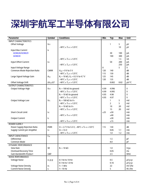
M ax UnitTypConditions M in Parameter SymbolINPUT CHARACTERISTICSOffset Voltage V OS1 5 μV−40°C ≤ T A ≤ +125°C 10 μVInput Bias Current I BAD8628/AD862930 100 pA AD8630 100 300 pA−40°C ≤ T A ≤ +125°C 1.5 nAInput Offset Current I OS50 200 pA−40°C ≤ T A ≤ +125°C 250 pAInput Voltage Range 0 5 V Common-Mode Rejection Ratio CMRR V CM = 0 V to 5 V 120 140 dB−40°C ≤ T A ≤ +125°C 115 130 dBLarge Signal Voltage Gain A VO R L = 10 kΩ, V O = 0.3 V to 4.7 V 125 145 dB−40°C ≤ T A ≤ +125°C 120 135 dBOffset Voltage Drift ∆V OS/∆T −40°C ≤ T A ≤ +125°C 0.002 0.02 μV/°C OUTPUT CHARACTERISTICSOutput Voltage High V OH R L = 100 kΩ to ground 4.99 4.996 V−40°C ≤ T A ≤ +125°C 4.99 4.995 VR L = 10 kΩ to ground 4.95 4.98 V−40°C ≤ T A ≤ +125°C 4.95 4.97 VOutput Voltage Low V OL R L = 100 kΩ to V+ 1 5 mV−40°C ≤ T A ≤ +125°C2 5 mVR L = 10 kΩ to V+ 10 20 mV−40°C ≤ T A ≤ +125°C15 20 mV Short-Circuit Limit I SC±25 ±50 mA−40°C ≤ T A ≤ +125°C±40 mAOutput Current I O±30 mA−40°C ≤ T A ≤ +125°C±15 mAPOWER SUPPLYPower Supply Rejection Ratio PSRR V S = 2.7 V to 5.5 V, −40°C ≤ T A ≤ +125°C 115 130 dBSupply Current per Amplifier I SY V O = V S/2 0.85 1.1 mA−40°C ≤ T A ≤ +125°C 1.0 1.2 mA INPUT CAPACITANCE C INDifferential 1.5 pFCommon Mode 8.0 pFDYNAMIC PERFORMANCESlew Rate SR R L = 10 kΩ 1.0 V/μsOverload Recovery Time 0.05 msGain Bandwidth Product GBP 2.5 MHzNOISE PERFORMANCEVoltage Noise e n p-p 0.1 Hz to 10 Hz 0.5 μV p-p0.1 Hz to 1.0 Hz 0.16 μV p-pVoltage Noise Density e n f = 1 kHz 22 nV/√Hz Current Noise Density i n f = 10 Hz 5 fA/√HzTYPICAL PERFORMANCE CHARACTERISTICSINPUT OFFSET VOLTAGE (µV)N U M B E R O F A M P L I F I E R S180160140120*********20002735-003Figure 5. Input Offset Voltage DistributionINPUT COMMON-MODE VOLTAGE (V)I N P U T B I A S C U R R E N T (p A )604050301020002735-004Figure 6. AD8628 Input Bias Current vs. Input Common-Mode VoltageINPUT COMMON-MODE VOLTAGE (V)I N P U T B I A S C U R R E N T (p A )150050010000–1000–500–150002735-005Figure 7. AD8628Input Bias Current vs. Input Common-Mode Voltage INPUT OFFSET VOLTAGE (µV)N U M B E R O F A M P L I F I E R S100809060704050102030002735-006Figure 8. Input Offset Voltage DistributionTCVOS (nV/°C)N U M B E R O F A M P L I F I E R S765432102735-007Figure 9. Input Offset Voltage DriftLOAD CURRENT (mA)O U T P U T V O L T A G E (m V )1k1001010.10.0102735-008Figure 10. Output Voltage to Supply Rail vs. Load CurrentFUNCTIONAL DESCRIPTIONThe AD8628/AD8629/AD8630 are single-supply, ultrahigh precision rail-to-rail input and output operational amplifiers. The typical offset voltage of less than 1 μV allows these amplifiers to be easily configured for high gains without risk of excessive output voltage errors. The extremely small temperature driftof 2 nV/°C ensures a minimum offset voltage error over their entire temperature range of −40°C to +125°C, making these amplifiers ideal for a variety of sensitive measurement applica-tions in harsh operating environments.The AD8628/AD8629/AD8630 achieve a high degree of precision through a patented combination of auto-zeroing and chopping. This unique topology allows the AD8628/AD8629/AD8630 to maintain their low offset voltage over a wide temperature range and over their operating lifetime. The AD8628/AD8629/AD8630 also optimize the noise and bandwidth over previous generations of auto-zero amplifiers, offering the lowest voltage noise of any auto-zero amplifier by more than 50%.Previous designs used either auto-zeroing or chopping to add precision to the specifications of an amplifier. Auto-zeroing results in low noise energy at the auto-zeroing frequency, at the expense of higher low frequency noise due to aliasing of wideband noise into the auto-zeroed frequency band. Chopping results in lower low frequency noise at the expense of larger noise energy at the chopping frequency. The AD8628/AD8629/AD8630 family uses both auto-zeroing and chopping in a patented ping-pong arrangement to obtain lower low frequency noise together with lower energy at the chopping and auto-zeroing frequencies, maximizing the signal-to-noise ratio for the majority of applications without the need for additional filtering. The relatively high clock frequency of 15 kHz simplifies filter requirements for a wide, useful noise-free bandwidth.The AD8628 is among the few auto-zero amplifiers offered in the 5-lead TSOT package. This provides a significant improvement over the ac parameters of the previous auto-zero amplifiers. The AD8628/AD8629/AD8630 have low noise over a relatively wide bandwidth (0 Hz to 10 kHz) and can be used where the highest dc precision is required. In systems with signal bandwidths of from 5 kHz to 10 kHz, the AD8628/AD8629/AD8630 provide true 16-bit accuracy, making them the best choice for very high resolution systems. 1/f NOISE1/f noise, also known as pink noise, is a major contributor to errors in dc-coupled measurements. This 1/f noise error term can be in the range of several μV or more, and, when amplified with the closed-loop gain of the circuit, can show up as a large output offset. For example, when an amplifier with a 5 μV p-p 1/f noise is configured for a gain of 1000, its output has 5 mV of error due to the 1/f noise. However, the AD8628/AD8629/AD8630 eliminate 1/f noise internally, thereby greatly reducing output errors.The internal elimination of 1/f noise is accomplished as follows. 1/f noise appears as a slowly varying offset to theAD8628/AD8629/ AD8630 inputs. Auto-zeroing corrects any dc or low frequency offset. Therefore, the 1/f noise component is essentially removed, leaving the AD8628/AD8629/AD8630 free of 1/f noise.One advantage that the AD8628/AD8629/AD8630 bring to system applications over competitive auto-zero amplifiers is their very low noise. The comparison shown in Figure 49 indicates an input-referred noise density of 19.4 nV/√Hz at 1 kHz for the AD8628, which is much better than the Competitor Aand Competitor B. The noise is flat from dc to 1.5 kHz, slowly increasing up to 20 kHz. The lower noise at low frequency is desirable where auto-zero amplifiers are widely used.2735-46FREQUENCY (kHz)VOLTAGENOISEDENSITY(nV/√Hz)120105907560453015Figure 49. Noise Spectral Density of AD8628 vs. CompetitionAD8628/AD8629/AD8630Data SheetPEAK-TO-PEAK NOISEBecause of the ping-pong action between auto-zeroing and chopping, the peak-to-peak noise of the AD8628/AD8629/ AD8630 is much lower than the competition. Figure 50 and Figure 51 show this comparison.TIME (1s/DIV)V O L T A G E (0.5µV /D I V )02735-047Figure 50. AD8628 Peak-to-Peak NoiseTIME (1s/DIV)V O L T A G E (0.5µV /D I V )02735-048Figure 51. Competitor A Peak-to-Peak NoiseNOISE BEHAVIOR WITH FIRST-ORDER, LOW-PASS FILTERThe AD8628 was simulated as a low-pass filter (see Figure 53) and then configured as shown in Figure 52. The behavior of the AD8628 matches the simulated data. It was verified that noise is rolled off by first-order filtering. Figure 53 and Figure 54 show the difference between the simulated and actual transferfunctions of the circuit shown in Figure 52.IN02735-049Figure 52. First-Order Low-Pass Filter Test Circuit,×101 Gain and 3 kHz Corner FrequencyFREQUENCY (kHz)N O I S E (d B )5045403530251510520030601009080705040201002735-050Figure 53. Simulation Transfer Function of the Test Circuit in Figure 52FREQUENCY (kHz)N O I S E (d B )5045403530251510520030601009080705040201002735-051Figure 54. Actual Transfer Function of the Test Circuit in Figure 52The measured noise spectrum of the test circuit charted in Figure 54 shows that noise between 5 kHz and 45 kHz is successfully rolled off by the first-order filter.TOTAL INTEGRATED INPUT-REFERRED NOISE FOR FIRST-ORDER FILTERFor a first-order filter, the total integrated noise from the AD8628 is lower than the noise of Competitor A.3dB FILTER BANDWIDTH (Hz)RM S N O I S E (µV )1010.102735-052Figure 55. RMS Noise vs. 3 dB Filter Bandwidth in HzData Sheet AD8628/AD8629/AD8630。
ZXMN6A08E6TA中文资料(Diodes)中文数据手册「EasyDatasheet - 矽搜」

pF pF VDS = 40V, V GS = 0V
f = 1MHz pF
nC VGS = 4.5V
SD0.01
I
0.2 0.4 0.6 0.8 1.0 1.2
VSD 源极 - 漏极电压(V)
源漏二极管正向电压
TJ结温(℃)
典型的传输特性
归 一 化 曲 线 V温 度
(Ω)
3V
1 T = 25°C
3.5V 4V 4.5V VGS
漏源导通电阻
0.1
DS(on)0.1 R
1
ID 漏电流(A)
导 通 电 阻 V漏 极 电 流
5V
7V 10V
10
10 T = 150°C
1
反向0漏.1电流(A)
T = 25°C
VGS = 0V
1.6
和V 1.4
VGS = 10V ID = 4.8A
RDS (on)
1
DS(o1n.)2
1.0
漏电0.流1 (A)
D
T = 25°C
正常0化.8ř
0.6 0.4 0.2
VGS (th)
VGS = VDS ID = 250uA
I 0.01
0.0
2
3
4
5
-50
0
50
100
150
VGS 门源电压(V)
超前信息 应用
• DC-DC转换器 • 电源管理功能 • 断开开关 • 电机控制
AD8628中文资料

PRELIMINARY TECHNICAL DATA Information furnished by Analog Devices is believed to be accurate and reliable.However, no responsibility is assumed by Analog Devices for its use, nor for any infringements of patents or other rights of third parties which may result from its use. No license is granted by implication or otherwise under any patent or patent rights of Analog Devices. One Technology Way, P.O. Box 9106, Norwood, MA 02062-9106, U.S.A. Tel: 617/329-4700World Wide Web Site: Fax: 617/326-8703© Analog Devices, Inc., 2002aZero-Drift, Single-Supply,Rail-to-Rail Input/Output Low Noise Operational AmplifierPreliminary Technical Data AD8628FEATURESLowest auto-zero amplifier noiseLow Offset Voltage: 5 µVInput Offset Drift: 0.03 µV/°CRail-to-Rail Input and Output Swing5 V Single-Supply OperationHigh Gain, CMRR, and PSRR: 120 dBVery Low Input Bias Current: 100 pALow Supply Current: 1.3 mAOverload Recovery Time: 0.2 msNo External Components RequiredAPPLICATIONSAutomotive SensorsPressure and Position SensorsStrain Gage AmplifiersMedical InstrumentationThermocouple AmplifiersGENERAL DESCRIPTIONThis new family of amplifiers has ultra-low offset, drift and bias current. The AD8628 is a wide bandwidth auto-zero amplifier featuring rail-to-rail input and output swings and low noise. Operation is fully specified from 2.7 to 5 volts single supply (±1.35V to ±2.5V dual supply).The AD8628 family provides the benefits previously found only in expensive auto-zeroing or chopper-stabilized amplifiers. Using Analog Devices’ new topology these zero-drift amplifiers combine low cost, with high accuracy and low noise. (No external capacitors are required.) In addition, the AD8628 greatly reduces the digital switching noise found in most chopper stabilized amplifiers.With an offset voltage of only 1µV, drift less than 0.005 µV/°C and noise of only 0.5uV P-P (0Hz to 10 Hz) the AD8628 is perfectly suited for applications where error sources cannot be tolerated. Position and pressure sensors, medical equipment, and strain gage amplifiers benefit greatly from nearly zero drift over their operating temperature range. Many systems may take advantage of the rail-to-rail input and output swings provided by the AD8628 family to reduce input biasing complexity and maximize SNR.The AD8628 family is specified for the extended industrial (-40° to +125°C) temperature range. The AD8628 amplifier is available in the tiny SOT23 and the popular 8-pin narrow SOIC plastic packages.5-Lead SOT(RT-5)8-Lead SO(R-8)AD8628AD8628SpecificationsPRELIMINARY TECHNICAL DATAAD8628– 2 – REV. PrA 1/29/02PRELIMINARY TECHNICAL DATAAD8628– 3 –SpecificationsPRELIMINARY TECHNICAL DATAAD8628– 4 – REV. PrA 1/29/02ABSOLUTE MAXIMUM RATINGSSupply Voltage..........................................................................+6V Input Voltage......................................................GND to Vs + 0.3V Differential Input Voltage 1.....................................................±5.0V Output Short-Circuit Duration to Gnd...............................Indefinite Storage Temperature RangeRT, R Package...............................................-65°C to +150°C Operating Temperature RangeAD8628.........................................................-40°C to +125°C Junction Temperature RangeRT, R Package...............................................-65°C to +150°C Lead Temperature Range (Soldering, 10 sec).......................+300°CNOTES1 Differential input voltage is limited to ±5.0 volts or the supply voltage, whichever is less.2 θJA is specified for the worst case conditions, i.e., θJAis specified for device in socket for P-DIP packages; θJA is specified for device soldered in circuit board for SOIC and TSSOP packages.ORDERING GUIDE。
TA3020中文资料
TECHNICAL INFORMATION
Stereo 300W (4Ω) Class-T Digital Audio Amplifier Driver using Digital Power ProcessingTM Technology TA3020
PRELIMINARY – January 2001
2
TA3020, Rev 2.1, 01.01
元器件交易网
TECHNICAL INFORMATION
Electrical Characteristics (Note 6)
TA = 25 °C. See Application/Test Circuit on page 7. Unless otherwise noted, the supply voltage is VPP=|VNN|=45V.
SYMBOL Iq PARAMETER Quiescent Current (No load, BBM0=1,BBM1=0, Mute = 0V) Mute Supply Current (No load, Mute = 5V) High-level input voltage (MUTE) Low-level input voltage (MUTE) High-level output voltage (HMUTE) IOH = 3mA Low-level output voltage (HMUTE) Output Offset Voltage Over Current Sense Voltage Threshold VPPSENSE Threshold Currents IOL = 3mA No Load, MUTE = Logic low 0.1% RFBA, RFBB, RFBC resistors TBD Over-voltage turn on (muted) Over-voltage turn off (mute off) Under-voltage turn off (mute off) Under-voltage turn on (muted) Over-voltage turn on (muted) Over-voltage turn off (mute off) Under-voltage turn off (mute off) Under-voltage turn on (muted) Over-voltage turn on (muted) Over-voltage turn off (mute off) Under-voltage turn off (mute off) Under-voltage turn on (muted) Over-voltage turn on (muted) Over-voltage turn off (mute off) Under-voltage turn off (mute off) Under-voltage turn on (muted) -TBD TBD TBD TBD TBD TBD TBD TBD TBD TBD 1.0 162 154 79 72 TBD TBD TBD TBD 174 169 86 77 TBD TBD TBD TBD 4.0 0.5 TBD TBD TBD TBD TBD TBD TBD TBD TBD TBD CONDITIONS VPP = +45V VNN = -45V V5 = 5V VN10 = 10V VPP = +45V VNN = -45V V5 = 5V VN10 = 10V 3.5 1.0 MIN. TYP. 90 90 45 200 1 1 20 1 MAX. UNITS mA mA mA mA mA mA mA mA V V V V mV V µA µA µA µA V V V V µA µA µA µA V V V V
AO4708资料

SymbolTyp Max 32406075R θJL 1724Maximum Junction-to-Ambient A Steady-State °C/W Maximum Junction-to-Lead CSteady-State°C/WThermal Characteristics ParameterUnits Maximum Junction-to-Ambient A t ≤ 10s R θJA °C/W AO4708AO4708SymbolMin TypMaxUnits BV DSS 30V V DS =24V, V GS =0V0.1T J =125°C20I GSS 0.1µA V GS(th)Gate Threshold Voltage 1.4 1.82.4V I D(ON)80A 7.28.7T J =125°C10.513.18.610.5m Ωg FS 85S V SD 0.390.5V I S5.5A C iss 28003360pF C oss 390pF C rss 145pF R g0.8 1.5ΩQ g (10V)4252nC Q g (4.5V)19nC Q gs 7nC Q gd 6nC t D(on)7ns t r 7ns t D(off)31ns t f 5ns t rr 1315ns Q rr12nCTHIS PRODUCT HAS BEEN DESIGNED AND QUALIFIED FOR THE CONSUMER MARKET. APPLICATIONS OR USES AS CRITICAL COMPONENTS IN LIFE SUPPORT DEVICES OR SYSTEMS ARE NOT AUTHORIZED. AOS DOES NOT ASSUME ANY LIABILITY ARISING Total Gate Charge VGS=10V, VDS=15V, ID=15AGate Drain Charge V GS =0V, V DS =15V, f=1MHz SWITCHING PARAMETERS Total Gate Charge Gate Source Charge Gate resistanceV GS =0V, V DS =0V, f=1MHzTurn-On Rise Time Turn-Off DelayTime V GS =10V, V DS =15V, R L =1Ω, R GEN =3ΩTurn-Off Fall TimeTurn-On DelayTime m ΩV GS =4.5V, I D =14AI S =1A,V GS =0V V DS =5V, I D =15AMaximum Body-Diode + Schottky Continuous CurrentInput Capacitance Output Capacitance DYNAMIC PARAMETERS R DS(ON)Static Drain-Source On-ResistanceForward TransconductanceDiode Forward VoltageV DS =V GS I D =250µA Electrical Characteristics (T J =25°C unless otherwise noted)STATIC PARAMETERS ParameterConditions I DSS Zero Gate Voltage Drain Current mA V DS =0V, V GS = ±12V Gate-Body leakage current Body Diode Reverse Recovery TimeBody Diode Reverse Recovery Charge I F =15A, dI/dt=300A/µsDrain-Source Breakdown Voltage On state drain currentI D =250uA, V GS =0V V GS =4.5V, V DS =5V V GS =10V, I D =15AReverse Transfer Capacitance I F =15A, dI/dt=300A/µsA: The value of R θJA is measured with the device in a still air environment with T A =25°C. The power dissipation P DSM and current rating I DSM are based on T J(MAX)=150°C, using t ≤ 10s junction-to-ambient thermal resistance.B: Repetitive rating, pulse width limited by junction temperature T J(MAX)=150°C.C. The R θJA is the sum of the thermal impedence from junction to lead R θJL and lead to ambient.D. The static characteristics in Figures 1 to 6 are obtained using <300 µs pulses, duty cycle 0.5% max.E. These tests are performed with the device mounted on 1 in 2 FR-4 board with 2oz. Copper, in a still air environment with T A =25°C. The SOA curve provides a single pulse rating. Rev0: Sept. 2006AO4708AO4708AO4708。
AD8638中文资料
16V Auto-Zero, Rail-to-Rail Output,Precision AmplifiersPreliminary Technical DataAD8638FEATURESLow Offset Voltage: 10 μV max. Offset Drift: 0.08 μV/°C Rail-to-Rail OutputRev. PrAInformation furnished by Analog Devices is believed to be accurate and reliable. However , no16V Single or ±8V Dual Supply Operation High Gain and CMRR: 140dB High PSRR: 140 dBVery Low Input Bias Current: 100 pA Low Supply Current: 1.4 mA/ampAPPLICATIONSPressure and Position Sensors Strain Gage Amplifiers Medical Instrumentation Thermocouple Amplifiers Automotive Sensors Precision ReferencesPrecision Current Source sGENERAL DESCRIPTIONThe AD8638 is a wide bandwidth auto-zero amplifiers featuring rail-to-rail output swing while operating from 5 V to 16 V single supply or +/−2.5 V to ±8V dual supplies.Using Analog Devices’ new topology these zero-drift amplifiers combine low cost, with high accuracy and low noise. No external capacitors are required. In addition, the AD8638 family greatly reduces the digital switching noise often found in chopper-stabilized amplifiers.With an offset voltage of 10 µV, offset drift less than 0.08 µV/°C and noise of only 1.5 µVp-p (0 Hz to 10 Hz), the AD8638 family is perfectly suited for applications where error sources must be minimized. Position and pressure sensors, thermocouple and thermopile detectors, and strain gage amplifiers benefit greatly from nearly zero drift over their operating temperature range.The AD8638 family is specified for the extended industrial (-40° to +125°C) temperature range. The AD8638 is available in SOT-23 and SOIC.PIN CONFIGURATIONS5- Lead SOT-23 (RJ-5 Suffix)OUT-INV+8- Lead SOIC (R-8 Suffix)NC -IN +IN V+ OUT NCNC NC = NO CONNECTNC = NO CONNECTAD8638 Preliminary Data Sheet ELECTRICAL CHARACTERISTICS (@ V S =16V, V CM = Vs/2, T A =+25°C unless otherwise specified.)AD8638 Preliminary Data Sheet ELECTRICAL CHARACTERISTICS (@ V S =5V, V CM = Vs/2, T A =+25°C unless otherwise specified.)AD8638 Preliminary Data SheetABSOLUTE MAXIMUM RATINGS1Supply voltage.........................................................................+16V Input Voltage.. (V)Differential Input Voltage1 (V)Output Short-Circuit Duration to Gnd..............................Indefinite Storage Temperature RangeR, RM, RU Packages.....................................-65°C to +150°C Operating Temperature RangeAD8638 .......................................................-40°C to +125°C Junction Temperature RangeR, RT Packages..............................................-65°C to +150°C Lead Temperature Range (Soldering, 60 Sec).....................+300°C1 Differential input voltage is limited to ±5V or the supply voltage whichever is less.2 θJA is specified for the worst case conditions, i.e., θJA is specified for device soldered in circuit board for surface mount packages.ORDERING GUIDEModel TemperatureRange Package Description Package Option AD8638ARJZ -40°C to +125°C 5-Lead SOT-23 RJ-5AD8638ARZ -40°C to +125°C 8-Lead SOIC_N R-8©2007 Analog Devices, Inc. All rights reserved. Trademarks andregistered trademarks are the property of their respective owners.PR06895-0-6/07(PrA)。
TA7678中文资料

TA7678LINEAR INTEGRATED CIRCUITVIDEO AND SOUND IF AMPLIFIER FOR MONOCHROME TV RECEIVERSDESCRIPTIONThe Contek TA7678is a monolithic integrated circuit designed for the VIF and SIF stage in B/W television receivers.The UTC TA7678is used for forward AGC Type.FEATUREVIF STAGE*High gain wide brand IF amplifier 50dB at 45MHz *Gain reduction with excellent stability:55dB at 45MHz *Excellent DG/DP and S/N characteristicsSIF STAGE*Excellent limiter characteristics *Excellent AM Rejection*Large undistorted audio output voltage with quadraturedetectorBLOCK DIAGRAMContekCONTEKTA7678LINEAR INTEGRATED CIRCUITCONTEKTA7678LINEAR INTEGRATED CIRCUITNote:1.V AGC =11.5V,VIF Input :45.5MHz,1kHz,30AM Modulation.Adjust VIF input Vi level so that the detected output of Pin 12with high impedance probe will be 0.8Vp-p and measure the input Level.2.V AGC =4V.Measure VIF input level vi is same as note 1D A=20log(Vi /Vi)(dB)3.VIF input :f=45.75MHz CW 15mVrms.Measure the DC level of Pin12.4.VIF Input :f=45.75MHz APL 100%.87.5%AM Modulation.Pin 14Open4.1.Adjust VIF inpt level 50mVp-p and measure the detected output level Vo(p-p)4.2.Then increase the input level so that the detected output level will be 1.1*Vo(p-p)and measure the inputlevel.5.V AGC =8V.VIF input :f=45.75MHz+-10MHz variable or sweep 15mVrms measure DC level of Pin12.6.V AGC =8V.SG1:45.75MHz CW.SG2:45.65~27MHz variable.6.1.Setting output of SG1s o that the DC level of Pin12will be6.2.Setting output of SG1(45.65MHz so that the AC level of Pin12will be 0.5Vp-p.6.3.Decreasing frequency of SG2until the AC level of Pin 12will be 0.35vp-p(-3dB of 0.5Vp-p)then readF SG2=F,f BW =45.75-F MHZ7.SG1:45.75MHz,1kHz 80%AM Modulation 100mVrms.SG2,SG3:OFF.Setting VAGC so that the output AC level of Pin12will be 2.7Vp-p.Measure CL of Pin12after setting to 0%AM of SG1.8.Measure 2ndof Pin12same as note 9.CONTEKTA7678LINEAR INTEGRATED CIRCUIT9.VAGC=8V.SG1:45.75MHz(P:picture)100mVrms,SG2:41.25MHz(S:Sound)32mVrms(-10dB of SG1),SG3:42.17MHz(C:Chroma)32mVrms(-10dB of SG1)9.1.Setting VAGC so that the output Pin12will be 3.0V DC.9.2.Measure the level difference between the C-level and 920kHz.10.V AGC =8V.VIF Input :f=45.75MHz video signal (RAMP)87.5%AM 100mVp-p.Setting ATT so that the SYNC TIP level of Pin12will be 2.5VDC measure DP and DG.11.V AGC =5V.f=45.75MHz.Measure RIN and CIN.12.S1=ON,S3=2,S5=1,S4=213.Pin 14open.VIF Input :45.75MHz CW 20mVrms.13.1.Adjust the voltate of Pin 3so that the voltage of Pin4will be 6.0V DC.13.2.Measure the Pin 3.14.Pin 14open.VIF Input:45.75MHz 100%APL 87.5%AM Modulation signal amplitude 50mVp-p mesure thedetected output voltage (white peak to SYNC TIP)15.PIN14:Op en.SG1:45.75MHz CW 100mvrms.SG2:41.25MHz CW 25mVrms.Measre SIF(4.5MHz)output voltage at Pin12.16.SIF input:f=4.5MHz FM fMOD=400HzmD f=+-25kHz16.1.Adjust SIF input level 100mVp-p and measure the detected output level Vos.16.2.Then decrease the i nput level so that the detected output level will be 3dB down ofVos and measure theinput level.17.SIF input:f=4.5MHz,FM fMOD=400Hz D f=+-25kHz.AM 30%,input level Vins=80dB m .18.SIF input:f=4.5MHz,fM fMOD=400HzD f=+-25kHz.Input level Vins=80dB m 19.SIF input:f=4.4~4.6MHz variable or sweep measure the outjput DC voltage change.20.SIF inptut :f=4.5MHz,FM FMOD=400HzD f=+-25kHz,input level Vins=80dB m .20.1.Measure the detected output voltagae vOA with Rx=.20.2.Then,adjust Rx so that the d etected output voltage will be VOA/2and measure Rx.1.DC TEST CIRCUITCONTEK元器件交易网TA7678LINEAR INTEGRATED CIRCUIT2.AC TESTS CIRCUIT3.VIDEO FREQUENCY RESPONSE&SIF OUTPUT VOLTAGE TEST CIRCUIT4.INTER MODULATION TEST CIRCUITCONTEKTA7678LINEAR INTEGRATED CIRCUIT5.DG,DP TEST CIRCUIT5.INPUT IMPEDANCETEST CIRCUITCONTEKTA7678LINEAR INTEGRATED CIRCUITUTCUNISONIC TECHNOLOGIES CO.,LTD.77.SIF INPUT IMPEDANCE TEST CIRCUIT8.V IN(LIM)AMR,V OD ,THD V OM TEST CIRCUIT9.AUDIO OUTPUT IMPEDANCE TEST CIRCUIT元器件交易网TA7678LINEAR INTEGRATED CIRCUITTYPICAL APPLICATION CIRCUITCONTEK。