AD8123ACPZ-R2中文资料
ADC12_A

18 ADC12_AADC12_A模块是一个高效的12位模—数转换器。
本章节将主要介绍MSP430 5XX单片机的ADC12_A模块。
18.1ADC12_A介绍ADC12_A模块支持高速的12位的模数转换。
该模块应用了包括一个12位的SAR内核,基准电压发生器(只有MSP430F54XX具备,在其他设备中应用的是REF模式)和一个16字的转换—控制缓冲器。
在没有CPU干预下,该缓冲器允许对16路独立采集而来的ADC信号进行转换和存储。
ADC12_A的特点有:最大转换速度超过200-ksps无数据丢失的单调的12位转换器采样—保持由采样周期控制,采样周期可通过设置软件或定时器确定利用软件,Timer_A或者Timer_B对采样进行初始换件选择芯片内部的基准电压发生器(对于MSP430F54XX为:1.5V或2.5V。
其他设备为:1.5V,2.0V或2.5V)软件选择外部或内部基准12路独立可配置的外部输入通道内部温度传感器转换通道,参考电压为AVcc和外部基准独立的选择通道基准源,包括正基准和负基准可选择的转换时钟源四种转换模式:单通道模式,重复单通道模式,序列模式和重复序列模式ADC内核和基准电压可以单独掉电(只有MSP430F54xx有此功能。
其他设备可以参考REF模块的说明)中断向量寄存器快速响应18路的ADC中断16位的转换结果存储寄存器图18-1所示为ADC12_A的方块图。
右图可知,MSP430F54xx中的基准电压发生器位于ADC12_A模块之中。
而其他设备中基准电压发生器常常存在于基准模块中。
详细内容可查阅相应的数据表。
A:MODOSC是综合时钟系统(UCS)中的部分内容。
详细内容可参考UCS部分。
图18-1.ADC12_A 方块图18.2ADC12_A运行ADC12_A模块由软件进行设置。
接下来,我们对ADC12_A的结构和操作进行讨论。
18.312位的ADC内核ADC内核将输入的模拟信号转换成一个12为的数字信号并将转换的结果存储到内存中。
ADC0808S125资料
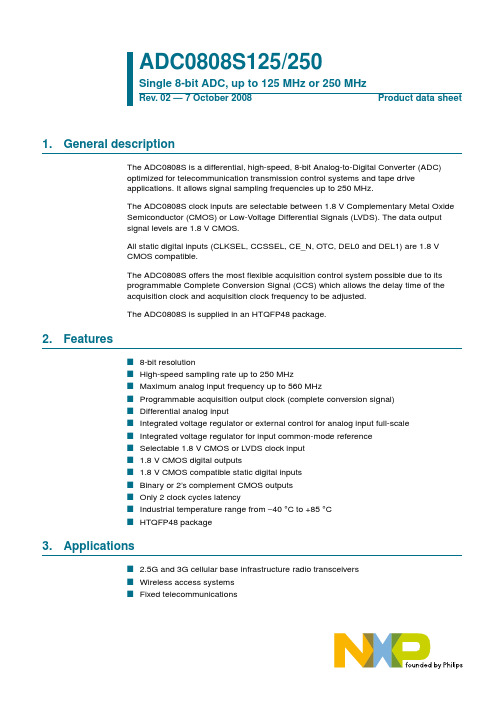
CLOCK DRIVER
ADC0808S
LATCH
17 26
CCS CCSSEL
IN INN
33 32
TRACK AND HOLD
8
RESISTOR LADDERS
ADC CORE
LATCH
8
D0 to D7 21 OTC
FSIN/ REFSEL
30 U/I LATCH
20
IR
INTERNAL REFERENCE
元器件交易网
ADC0808S125/250
Single 8-bit ADC, up to 125 MHz or 250 MHz
Rev. 02 — 7 October 2008 Product data sheet
1. General description
The ADC0808S is a differential, high-speed, 8-bit Analog-to-Digital Converter (ADC) optimized for telecommunication transmission control systems and tape drive applications. It allows signal sampling frequencies up to 250 MHz. The ADC0808S clock inputs are selectable between 1.8 V Complementary Metal Oxide Semiconductor (CMOS) or Low-Voltage Differential Signals (LVDS). The data output signal levels are 1.8 V CMOS. All static digital inputs (CLKSEL, CCSSEL, CE_N, OTC, DEL0 and DEL1) are 1.8 V CMOS compatible. The ADC0808S offers the most flexible acquisition control system possible due to its programmable Complete Conversion Signal (CCS) which allows the delay time of the acquisition clock and acquisition clock frequency to be adjusted. The ADC0808S is supplied in an HTQFP48 package.
ADC12138CIMSA资料
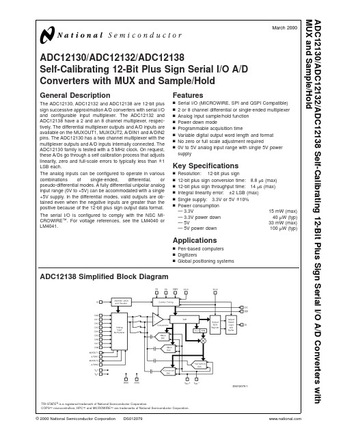
ADC12130/ADC12132/ADC12138Self-Calibrating 12-Bit Plus Sign Serial I/O A/D Converters with MUX and Sample/HoldGeneral DescriptionThe ADC12130,ADC12132and ADC12138are 12-bit plus sign successive approximation A/D converters with serial I/O and configurable input multiplexer.The ADC12132and ADC12138have a 2and an 8channel multiplexer,respec-tively.The differential multiplexer outputs and A/D inputs are available on the MUXOUT1,MUXOUT2,A/DIN1and A/DIN2pins.The ADC12130has a two channel multiplexer with the multiplexer outputs and A/D inputs internally connected.The ADC12130family is tested with a 5MHz clock.On request,these A/Ds go through a self calibration process that adjusts linearity,zero and full-scale errors to typically less than ±1LSB each.The analog inputs can be configured to operate in various combinations of single-ended,differential,or pseudo-differential modes.A fully differential unipolar analog input range (0V to +5V)can be accommodated with a single +5V supply.In the differential modes,valid outputs are ob-tained even when the negative inputs are greater than the positive because of the 12-bit plus sign output data format.The serial I/O is configured to comply with the NSC MI-CROWIRE ™.For voltage references,see the LM4040or LM4041.Featuresn Serial I/O (MICROWIRE,SPI and QSPI Compatible)n 2or 8channel differential or single-ended multiplexer n Analog input sample/hold function n Power down moden Programmable acquisition timen Variable digital output word length and format n No zero or full scale adjustment requiredn0V to 5V analog input range with single 5V power supplyKey Specificationsn Resolution:12-bit plus signn 12-bit plus sign conversion time:8.8µs (max)n 12-bit plus sign throughput time:14µs (max)n Integral linearity error:±2LSB (max)n Single supply: 3.3V or 5V ±10%nPower consumption —3.3V 15mW (max)—3.3V power down 40µW (typ)—5V 33mW (max)—5V power down 100µW (typ)Applicationsn Pen-based computers n Digitizersn Global positioning systemsADC12138Simplified Block DiagramTRI-STATE ®is a registered trademark of National Semiconductor Corporation.COPS ™microcontrollers,HPC ™and MICROWIRE ™are trademarks of National Semiconductor Corporation.DS012079-1March 2000ADC12130/ADC12132/ADC12138Self-Calibrating 12-Bit Plus Sign Serial I/O A/D Converters with MUX and Sample/Hold©2000National Semiconductor Corporation Ordering InformationIndustrial Temperature Range−40˚C ≤T A ≤+85˚C NS Package Number ADC12130CIN N16E,Dual-In-Line ADC12130CIWM M16B,Wide Body SOADC12132CIMSA MSA20,SSOP ADC12138CIN N28B,Dual-In-LineADC12138CIWM M28B ADC12138CIMSAMSA28,SSOPConnection Diagrams16-Pin Dual-In-Line and Wide Body SO PackagesDS012079-2Top View20-Pin SSOP PackageDS012079-47Top View28-Pin Dual-In-Line,SSOP and Wide Body SO PackagesDS012079-3Top ViewA D C 12130/A D C 12132/A D C 12138 2Pin DescriptionsCCLK The clock applied to this input controls the su-cessive approximation conversion time intervaland the acquisition time.The rise and fall timesof the clock edges should not exceed1µs. SCLK This is the serial data clock input.The clock applied to this input controls the rate at whichthe serial data exchange occurs.The risingedge loads the information on the DI pin intothe multiplexer address and mode select shiftregister.This address controls which channelof the analog input multiplexer(MUX)is se-lected and the mode of operation for the A/D.With CS low,the falling edge of SCLK shiftsthe data resulting from the previous ADC con-version out on DO,with the exception of thefirst bit of data.When CS is low continuously,the first bit of the data is clocked out on the ris-ing edge of EOC(end of conversion).WhenCS is toggled,the falling edge of CS alwaysclocks out the first bit of data.CS should bebrought low when SCLK is low.The rise andfall times of the clock edges should not exceed1µs.DI This is the serial data input pin.The data ap-plied to this pin is shifted by the rising edge ofSCLK into the multiplexer address and modeselect register.Table2through Table4showthe assignment of the multiplexer address andthe mode select data.DO The data output pin.This pin is an active push/ pull output when CS is low.When CS is high,this output is TRI-STATE.The A/D conversionresult(DB0–DB12)and converter status dataare clocked out by the falling edge of SCLK onthis pin.The word length and format of this re-sult can vary(see Table1).The word lengthand format are controlled by the data shiftedinto the multiplexer address and mode selectregister(see Table4).EOC This pin is an active push/pull output and indi-cates the status of the ADC12130/2/8.Whenlow,it signals that the A/D is busy with a con-version,auto-calibration,auto-zero or powerdown cycle.The rising edge of EOC signalsthe end of one of these cycles.CS This is the chip select pin.When a logic low is applied to this pin,the rising edge of SCLKshifts the data on DI into the address register.This low also brings DO out of TRI-STATE.With CS low,the falling edge of SCLK shiftsthe data resulting from the previous ADC con-version out on DO,with the exception of thefirst bit of data.When CS is low continuously,the first bit of the data is clocked out on the ris-ing edge of EOC(end of conversion).WhenCS is toggled,the falling edge of CS alwaysclocks out the first bit of data.CS should bebrought low when SCLK is low.The fallingedge of CS resets a conversion in progressand starts the sequence for a new conversion.When CS is brought back low during a conver-sion,that conversion is prematurely termi-nated.The data in the output latches may becorrupted.Therefore,when CS is brought backlow during a conversion in progress the dataoutput at that time should be ignored.CS mayalso be left continuously low.In this case it isimperative that the correct number of SCLKpulses be applied to the ADC in order to re-main synchronous.After the ADC supplypower is applied it expects to see13clockpulses for each I/O sequence.The number ofclock pulses the ADC expects is the same asthe digital output word length.This word lengthcan be modified by the data shifted in on theDO pin.Table4details the data required.DOR This is the data output ready pin.This pin is anactive push/pull output.It is low when the con-version result is being shifted out and goeshigh to signal that all the data has been shiftedout.CONV A logic low is required on this pin to programany mode or change the ADC’s configurationas listed in the Mode Programming Table(Table4)such as12-bit conversion,Auto Cal,Auto Zero etc.When this pin is high the ADC isplaced in the read data only mode.While in theread data only mode,bringing CS low andpulsing SCLK will only clock out on DO anydata stored in the ADCs output shift register.The data on DI will be neglected.A new con-version will not be started and the ADC will re-main in the mode and/or configuration previ-ously programmed.Read data only cannot beperformed while a conversion,Auto-Cal orAuto-Zero are in progress.PD This is the power down pin.When PD is highthe A/D is powered down;when PD is low theA/D is powered up.The A/D takes a maximumof700µs to power up after the command isgiven.CH0–CH7These are the analog inputs of the MUX.Achannel input is selected by the address infor-mation at the DI pin,which is loaded on the ris-ing edge of SCLK into the address register(see Table2and Table3).The voltage applied to these inputs should notexceed V A+or go below GND.Exceeding thisrange on an unselected channel will corruptthe reading of a selected channel.COM This pin is another analog input pin.It is usedas a pseudo ground when the analog multi-plexer is single-ended.MUXOUT1,MUXOUT2These are the multiplexer outputpins.A/DIN1,A/DIN2These are the converter input pins.MUXOUT1is usually tied to A/DIN1.MUXOUT2is usuallytied to A/DIN2.If external circuitry is placed be-tween MUXOUT1and A/DIN1,or MUXOUT2and A/DIN2it may be necessary to protectthese pins.The voltage at these pins shouldnot exceed V A+or go below AGND(see Figure5).V REF+This is the positive analog voltage referenceinput.In order to maintain accuracy,the volt-age range of V REF(V REF=V REF+−V REF−)isADC12130/ADC12132/ADC121383Pin Descriptions(Continued)1V DC to 5.0V DC and the voltage at V REF +cannot exceed V A +.See Figure 6for recom-mended bypassing.V REF −The negative voltage reference input.In order to maintain accuracy,the voltage at this pin must not go below GND or exceed V A +.(See Figure 6).V A +,V D +These are the analog and digital power supply pins.V A +and V D +are not connected together on the chip.These pins should be tied to the same power supply and bypassed separately (see Figure 6).The operating voltage range of V A +and V D +is 3.0V DC to 5.5V DC .DGND This is the digital ground pin (see Figure 6).AGNDThis is the analog ground pin (see Figure 6).A D C 12130/A D C 12132/A D C 12138 4Absolute Maximum Ratings (Notes 1,2)If Military/Aerospace specified devices are required,please contact the National Semiconductor Sales Office/Distributors for availability and specifications.Positive Supply Voltage (V +=V A +=V D +)6.5VVoltage at Inputs and Outputs except CH0–CH7and COM −0.3V to V ++0.3V Voltage at Analog Inputs CH0–CH7and COM GND −5V to V ++5V|V A +−V D +|300mV Input Current at Any Pin (Note 3)±30mA Package Input Current (Note 3)±120mAPackage Dissipation at T A =25˚C (Note 4)500mWESD Susceptability (Note 5)Human Body Model 1500V Soldering InformationN Packages (10seconds)260˚C SO Package (Note 6):Vapor Phase (60seconds)215˚C Infrared (15seconds)220˚CStorage Temperature −65˚C to +150˚COperating Ratings (Notes 1,2)Operating Temperature RangeT MIN ≤T A ≤T MAXADC12130CIN,ADC12130CIWM,ADC12132CIMSA,ADC12138CIMSA,ADC12138CIN,ADC12138CIWM −40˚C ≤T A ≤+85˚CSupply Voltage (V +=V A +=V D +)+3.0V to +5.5V|V A +−V D +|≤100mV V REF +0V to V A +V REF −0V to V REF +V REF (V REF +−V REF −)1V to V A +V REF Common Mode Voltage Range0.1V A +to 0.6V A +A/DIN1,A/DIN2,MUXOUT1and MUXOUT2Voltage Range 0V to V A +A/D IN Common Mode Voltage Range0V to V A +Converter Electrical CharacteristicsThe following specifications apply for (V +=V A +=V D +=+5V,V REF +=+4.096V,and fully differential input with fixed 2.048V common-mode voltage)or (V +=V A +=V D +=3.3V,V REF +=2.5V and fully-differential input with fixed 1.250Vcommon-mode voltage),V REF −=0V,12-bit +sign conversion mode,source impedance for analog inputs,V REF −and V REF +≤25Ω,f CK =f SK =5MHz,and 10(t CK )acquisition time unless otherwise specified.Boldface limits apply for T A =T J =T MIN to T MAX ;all other limits T A =T J =25˚C.(Notes 7,8,9)SymbolParameterConditionsTypical (Note 10)Limits Units (Limits)(Note 11)STATIC CONVERTER CHARACTERISTICSResolution12+signBits (min)+ILE Positive Integral Linearity Error After Auto-Cal (Notes 12,18)±1/2±2LSB (max)−ILE Negative Integral Linearity Error After Auto-Cal (Notes 12,18)±1/2±2LSB (max)DNLDifferential Non-Linearity After Auto-Cal±1.5LSB (max)Positive Full-Scale Error After Auto-Cal (Notes 12,18)±1/2±3.0LSB (max)Negative Full-Scale Error After Auto-Cal (Notes 12,18)±1/2±3.0LSB (max)Offset ErrorAfter Auto-Cal (Notes 5,18)±1/2±2LSB (max)V IN (+)=V IN (−)=2.048VDC Common Mode ErrorAfter Auto-Cal (Note 15)±2LSB (max)TUETotal Unadjusted ErrorAfter Auto-Cal ±1LSB(Notes 12,13,14)ADC12130/ADC12132/ADC121385Converter Electrical CharacteristicsThe following specifications apply for (V +=V A +=V D +=+5V,V REF +=+4.096V,and fully differential input with fixed 2.048V common-mode voltage)or (V +=V A +=V D +=3.3V,V REF +=+2.5V and fully-differential input with fixed 1.250Vcommon-mode voltage),V REF −=0V,12-bit +sign conversion mode,source impedance for analog inputs,V REF −and V REF +≤25Ω,f CK =f SK =5MHz,and 10(t CK )acquisition time unless otherwise specified.Boldface limits apply for T A =T J =T MIN to T MAX ;all other limits T A =T J =25˚C.(Notes 7,8,9)(Continued)SymbolParameterConditionsTypical (Note 10)Limits Units (Limits)(Note 11)STATIC CONVERTER CHARACTERISTICS (Continued)Multiplexer Channel to Channel ±0.05LSBMatchingPower Supply SensitivityV +=+5V ±10%V REF =+4.096VOffset Error ±0.5LSB +Full-Scale Error ±0.5LSB −Full-Scale Error±0.5LSB +Integral Linearity Error ±0.5LSB −Integral Linearity Error±0.5LSBUNIPOLAR DYNAMIC CONVERTER CHARACTERISTICS S/(N+D)Signal-to-Noise Plus f IN =1kHz,V IN =5V PP ,V REF +=5.0V 69.4dB Distortion Ratiof IN =20kHz,V IN =5V PP ,V REF +=5.0V 68.3dB f IN =40kHz,V IN =5V PP ,V REF +=5.0V 65.7dB −3dB Full Power BandwidthV IN =5V PP ,where S/(N+D)drops 3dB 31kHzDIFFERENTIAL DYNAMIC CONVERTER CHARACTERISTICSS/(N+D)Signal-to-Noise Plus f IN =1kHz,V IN =±5V,V REF +=5.0V 77.0dB Distortion Ratiof IN =20kHz,V IN =±5V,V REF +=5.0V 73.9dB f IN =40kHz,V IN =±5V,V REF +=5.0V 67.0dB −3dB Full Power BandwidthV IN =±5V,where S/(N+D)drops 3dB40kHzElectrical CharacteristicsThe following specifications apply for (V +=V A +=V D +=+5V,V REF +=+4.096V,and fully differential input with fixed 2.048V common-mode voltage)or (V +=V A +=V D +=+3.3V,V REF +=2.5V and fully-differential input with fixed 1.250Vcommon-mode voltage),V REF −=0V,12-bit +sign conversion mode,source impedance for analog inputs,V REF −and V REF +≤25Ω,f CK =f SK =5MHz,and 10(t CK )acquisition time unless otherwise specified.Boldface limits apply for T A =T J =T MIN to T MAX ;all other limits T A =T J =25˚C.(Notes 7,8,9)SymbolParameterConditionsTypical Limits Units (Note 10)(Note 11)(Limits)REFERENCE INPUT,ANALOG INPUTS AND MULTIPLEXER CHARACTERISTICS C REF Reference Input Capacitance 85pF C A/DA/DIN1and A/DIN2Analog Input 75pF CapacitanceA/DIN1and A/DIN2Analog Input V IN =+5.0V or ±0.1µALeakage CurrentV IN =0VCH0–CH7and COM Input VoltageGND −0.05VV A ++0.05C CH CH0–CH7and COM Input Capacitance10pF C MUXOUTMUX Output Capacitance 20pF Off Channel Leakage (Note 16)On Channel =5V and −0.01µA CH0–CH7and COM PinsOff Channel =0V On Channel =0V and 0.01µAOff Channel =5VA D C 12130/A D C 12132/A D C 12138 6Electrical Characteristics(Continued)The following specifications apply for(V+=V A+=V D+=+5V,V REF+=+4.096V,and fully differential input with fixed2.048V common-mode voltage)or(V+=V A+=V D+=+3.3V,V REF+=2.5V and fully-differential input with fixed1.250Vcommon-mode voltage),V REF−=0V,12-bit+sign conversion mode,source impedance for analog inputs,V REF−and V REF+≤25Ω,f CK=f SK=5MHz,and10(t CK)acquisition time unless otherwise specified.Boldface limits apply for T A=T J=T MIN to T MAX;all other limits T A=T J=25˚C.(Notes7,8,9)Symbol Parameter Conditions Typical Limits Units(Note10)(Note11)(Limits) REFERENCE INPUT,ANALOG INPUTS AND MULTIPLEXER CHARACTERISTICSOn Channel Leakage(Note16)On Channel=5V and0.01µACH0–CH7and COM Pins Off Channel=0VOn Channel=0V and−0.01µAOff Channel=5VMUXOUT1and MUXOUT2V MUXOUT=5.0V or0.01µALeakage Current V MUXOUT=0VR ON MUX On Resistance V IN=2.5V and8501900Ω(max)V MUXOUT=2.4VR ON Matching Channel to Channel V IN=2.5V and5%V MUXOUT=2.4VChannel to Channel Crosstalk V IN=5V PP,f IN=40kHz−72dBMUX Bandwidth90kHz DC and Logic Electrical CharacteristicsThe following specifications apply for(V+=V A+=V D+=+5V,V REF+=+4.096V,and fully-differential input with fixed2.048V common-mode voltage)or(V+=V A+=V D+=+3.3V,V REF+=+2.5V and fully-differential input with fixed1.250Vcommon-mode voltage),V REF−=0V,12-bit+sign conversion mode,source impedance for analog inputs,V REF−and V REF+≤25Ω,f CK=f SK=5MHz,and10(t CK)acquisition time unless otherwise specified.Boldface limits apply for T A=T J=T MIN to T MAX;all other limits T A=T J=25˚C.(Notes7,8,9)Symbol Parameter Conditions Typical(Note10)V+=V A+=V+=V A+=Units(Limits) V D+=3.3V V D+=5VLimits Limits(Note11)(Note11)CCLK,CS,CONV,DI,PD AND SCLK INPUT CHARACTERISTICSV IN(1)Logical“1”InputVoltageV A+=V D+=V++10% 2.0 2.0V(min)V IN(0)Logical“0”InputVoltageV A+=V D+=V+−10%0.80.8V(max)I IN(1)Logical“1”InputCurrentV IN=V+0.005 1.0 1.0µA(max)I IN(0)Logical“0”InputCurrentV IN=0V−0.005−1.0−1.0µA(min) DO,EOC AND DOR DIGITAL OUTPUT CHARACTERISTICSV OUT(1)Logical“1”V A+=V D+=V+−10%,Output Voltage I OUT=−360µA 2.4 2.4V(min)V A+=V D+=V+−10%, 2.9 4.25V(min)I OUT=−10µAV OUT(0)Logical“0”V A+=V D+=V+−10%Output Voltage I OUT=1.6mA0.40.4V(max) I OUT TRI-STATE V OUT=0V−0.1−3.0−3.0µA(max)Output Current V OUT=V+−0.1 3.0 3.0+I SC Output ShortCircuit SourceCurrent V OUT=0V−14mAADC12130/ADC12132/ADC121387DC and Logic Electrical Characteristics(Continued)The following specifications apply for (V +=V A +=V D +=+5V,V REF +=+4.096V,and fully-differential input with fixed 2.048V common-mode voltage)or (V +=V A +=V D +=+3.3V,V REF +=+2.5V and fully-differential input with fixed 1.250Vcommon-mode voltage),V REF −=0V,12-bit +sign conversion mode,source impedance for analog inputs,V REF −and V REF +≤25Ω,f CK =f SK =5MHz,and 10(t CK )acquisition time unless otherwise specified.Boldface limits apply for T A =T J =T MIN to T MAX ;all other limits T A =T J =25˚C.(Notes 7,8,9)SymbolParameterConditionsTypical (Note 10)V +=V A +=V +=V A +=Units (Limits)V D +=3.3V V D +=5V Limits Limits (Note 11)(Note 11)DO,EOC AND DOR DIGITAL OUTPUT CHARACTERISTICS −I SCOutput Short Circuit Sink Current V OUT =V D +16mAPOWER SUPPLY CHARACTERISTICS I D +Digital Supply 1.52.5mA (max)CurrentCS =HIGH,Powered Down,CCLK on 600µA CS =HIGH,Powered Down,CCLK off20µA I A +Positive Analog 3.04.0mA (max)Supply CurrentCS =HIGH,Powered Down,CCLK on 10µA CS =HIGH,Powered Down,CCLK off0.1µAI REFReference Input CurrentCS =HIGH,Powered Down,CCLK on 70µA CS =HIGH,Powered Down,CCLK off0.1µAAC Electrical CharacteristicsThe following specifications apply for (V +=V A +=V D +=+5V,V REF +=+4.096V,and fully-differential input with fixed 2.048V common-mode voltage)or (V +=V A +=V D +=+3.3V,V REF +=+2.5V and fully-differential input with fixed 1.250Vcommon-mode voltage),V REF −=0V,12-bit +sign conversion mode,source impedance for analog inputs,V REF −and V REF +≤25Ω,f CK =f SK =5MHz,and 10(t CK )acquisition time unless otherwise specified.Boldface limits apply for T A =T J =T MIN to T MAX ;all other limits T A =T J =25˚C.(Note 17)SymbolParameterConditionsTypical Limits Units (Note 10)(Note 11)(Limits)f CK Conversion Clock 105MHz (max)(CCLK)Frequency 1MHz (min)f SKSerial Data Clock 105MHz (max)SCLK Frequency 0Hz (min)Conversion Clock 40%(min)Duty Cycle 60%(max)Serial Data Clock 40%(min)Duty Cycle60%(max)t CConversion Time12-Bit +Sign or 12-Bit44(t CK )44(t CK )(max)8.8µs (max)A D C 12130/A D C 12132/A D C 12138 8AC Electrical Characteristics(Continued)The following specifications apply for(V+=V A+=V D+=+5V,V REF+=+4.096V,and fully-differential input with fixed2.048V common-mode voltage)or(V+=V A+=V D+=+3.3V,V REF+=+2.5V and fully-differential input with fixed1.250Vcommon-mode voltage),V REF−=0V,12-bit+sign conversion mode,source impedance for analog inputs,V REF−and V REF+≤25Ω,f CK=f SK=5MHz,and10(t CK)acquisition time unless otherwise specified.Boldface limits apply for T A=T J=T MIN to T MAX;all other limits T A=T J=25˚C.(Note17)Symbol Parameter Conditions Typical Limits Units(Note 10)(Note11)(Limits)t A Acquisition Time6Cycles Programmed6(t CK)6(t CK)(min) (Note19)7(t CK)(max)1.2µs(min)1.4µs(max)10Cycles Programmed10(t CK)10(t CK)(min)11(t CK)(max)2.0µs(min)2.2µs(max)18Cycles Programmed18(t CK)18(t CK)(min)19(t CK)(max)3.6µs(min)3.8µs(max)34Cycles Programmed34(t CK)34(t CK)(min)35(t CK)(max)6.8µs(min)7.0µs(max)t CAL Self-Calibration Time4944(t CK)4944(t CK)(max)988.8µs(max)t AZ Auto-Zero Time76(t CK)76(t CK)(max)15.2µs(max)t SYNC Self-Calibration or2(t CK)2(t CK)(min) Auto-Zero Synchronization3(t CK)(max)Time from DOR0.40µs(min)0.60µs(max)t DOR DOR High Time when CS is Low9(t SK)9(t SK)(max) Continuously for Read Data and SoftwarePower Up/Down1.8µs(max)t CONV CONV Valid Data Time8(t SK)8(t SK)(max)1.6µs(max)AC Electrical CharacteristicsThe following specifications apply for(V+=V A+=V D+=+5V,V REF+=+4.096V,and fully-differential input with fixed2.048V common-mode voltage)or(V+=V A+=V D+=+3.3V,V REF+=+2.5V and fully-differential input with fixed1.250Vcommon-mode voltage),V REF−=0V,12-bit+sign conversion mode,source impedance for analog inputs,V REF−and V REF+≤25Ω,f CK=f SK=5MHz,and10(t CK)acquisition time unless otherwise specified.Boldface limits apply for T A=T J=T MIN to T MAX;all other limits T A=T J=25˚C.(Note17)(Continued)Symbol Parameter Conditions Typical Limits Units(Note10)(Note11)(Limits)t HPU Hardware Power-Up Time,Time from500700µs(max) PD Falling Edge to EOC Rising Edget SPU Software Power-Up Time,Time fromSerial Data Clock Falling Edge to500700µs(max)EOC Rising Edget ACC Access Time Delay from2560ns(max) CS Falling Edge to DO Data ValidADC12130/ADC12132/ADC121389AC Electrical Characteristics(Continued)The following specifications apply for (V +=V A +=V D +=+5V,V REF +=+4.096V,and fully-differential input with fixed 2.048V common-mode voltage)or (V +=V A +=V D +=+3.3V,V REF +=+2.5V and fully-differential input with fixed 1.250Vcommon-mode voltage),V REF −=0V,12-bit +sign conversion mode,source impedance for analog inputs,V REF −and V REF +≤25Ω,f CK =f SK =5MHz,and 10(t CK )acquisition time unless otherwise specified.Boldface limits apply for T A =T J =T MIN to T MAX ;all other limits T A =T J =25˚C.(Note 17)(Continued)Symbol ParameterConditionsTypical Limits Units (Note 10)(Note 11)(Limits)t SET-UP Set-Up Time of CS Falling Edge to 50ns (min)Serial Data Clock Rising Edge t DELAY Delay from SCLK Falling 05ns (min)Edge to CS Falling Edge t 1H ,t 0H Delay from CS Rising Edge to R L =3k,C L =100pF70100ns (max)DO TRI-STATE ®t HDI DI Hold Time from Serial Data 515ns (min)Clock Rising Edget SDI DI Set-Up Time from Serial Data 510ns (min)Clock Rising Edget HDO DO Hold Time from Serial Data R L =3k,C L =100pF3565ns (max)Clock Falling Edge5ns (min)t DDO Delay from Serial Data Clock 5090ns (max)Falling Edge to DO Data Valid t RDO DO Rise Time,TRI-STATE to High R L =3k,C L =100pF1040ns (max)DO Rise Time,Low to High 1040ns (max)t FDO DO Fall Time,TRI-STATE to Low R L =3k,C L =100pF 1540ns (max)DO Fall Time,High to Low 1540ns (max)t CD Delay from CS Falling Edge 4580ns (max)to DOR Falling Edget SD Delay from Serial Data Clock Falling 4580ns (max)Edge to DOR Rising Edge C IN Capacitance of Logic Inputs 10pF C OUTCapacitance of Logic Outputs20pFNote 1:Absolute Maximum Ratings indicate limits beyond which damage to the device may occur.Operating Ratings indicate conditions for which the device is func-tional,but do not guarantee specific performance limits.For guaranteed specifications and test conditions,see the Electrical Characteristics.The guaranteed speci-fications apply only for the test conditions listed.Some performance characteristics may degrade when the device is not operated under the listed test conditions.Note 2:All voltages are measured with respect to GND,unless otherwise specified.Note 3:When the input voltage (V IN )at any pin exceeds the power supplies (V IN <GND or V IN >V A +or V D +),the current at that pin should be limited to 30mA.The 120mA maximum package input current rating limits the number of pins that can safely exceed the power supplies with an input current of 30mA to four.Note 4:The maximum power dissipation must be derated at elevated temperatures and is dictated by T J max,θJA and the ambient temperature,T A .The maximum allowable power dissipation at any temperature is P D =(T J max −T A )/θJA or the number given in the Absolute Maximum Ratings,whichever is lower.For this device,T J max =150˚C.The typical thermal resistance (θJA )of these parts when board mounted follow:ThermalPart Number ResistanceθJA ADC12130CIN 53˚C/W ADC12130CIWM 70˚C/W ADC12132CIMSA 134˚C/W ADC12138CIN 40˚C/W ADC12138CIWM 50˚C/W ADC12138CIMSA125˚C/WNote 5:The human body model is a 100pF capacitor discharged through a 1.5k Ωresistor into each pin.Note 6:See AN450“Surface Mounting Methods and Their Effect on Product Reliability”or the section titled “Surface Mount”found in any post 1986National Semi-conductor Linear Data Book for other methods of soldering surface mount devices.A D C 12130/A D C 12132/A D C 12138 10AC Electrical Characteristics(Continued)Note 7:Two on-chip diodes are tied to each analog input through a series resistor as shown below.Input voltage magnitude up to 5V above V A +or 5V below GND will not damage this device.However,errors in the A/D conversion can occur (if these diodes are forward biased by more than 50mV)if the input voltage magnitude of selected or unselected analog input go above V A +or below GND by more than 50mV.As an example,if V A +is 4.5V DC ,full-scale input voltage must be ≤4.55V DC to ensure accurate conversions.Note 8:To guarantee accuracy,it is required that the V A +and V D +be connected together to the same power supply with separate bypass capacitors at each V +pin.Note 9:With the test condition for V REF (V REF +−V REF −)given as +4.096V,the 12-bit LSB is 1.0mV.For V REF =2.5V,the 12-bit LSB is 610µV.Note 10:Typicals are at T J =T A =25˚C and represent most likely parametric norm.Note 11:Tested limits are guaranteed to National’s AOQL (Average Outgoing Quality Level).Note 12:Positive integral linearity error is defined as the deviation of the analog value,expressed in LSBs,from the straight line that passes through positive full-scale and zero.For negative integral linearity error,the straight line passes through negative full-scale and zero (see Figure 2and Figure 3).Note 13:Zero error is a measure of the deviation from the mid-scale voltage (a code of zero),expressed in LSB.It is the average value of the code transitions be-tween −1to 0and 0to +1(see Figure 4).Note 14:Total unadjusted error includes offset,full-scale,linearity and multiplexer errors.Note 15:The DC common-mode error is measured in the differential multiplexer mode with the assigned positive and negative input channels shorted together.Note 16:Channel leakage current is measured after the channel selection.Note 17:Timing specifications are tested at the TTL logic levels,V OL =0.4V for a falling edge and V OL =2.4V for a rising edge.TRI-STATE output voltage is forced to 1.4V.Note 18:The ADC12130family’s self-calibration technique ensures linearity and offset errors as specified,but noise inherent in the self-calibration process will re-sult in a maximum repeatability uncertainty of 0.2LSB.Note 19:If SCLK and CCLK are driven from the same clock source,then t A is 6,10,18or 34clock periods minimum and maximum.Note 20:The “12-Bit Conversion of Offset”and “12-Bit Conversion of Full-Scale”modes are intended to test the functionality of the device.Therefore,the output data from these modes are not an indication of the accuracy of a conversion result.DS012079-4DS012079-5FIGURE 1.Transfer CharacteristicADC12130/ADC12132/ADC12138。
AD12250A中文资料

AD12250A
input signals into 24-bit I2S digital audio data through on-chip anti-aliasing filter, multi-bit Σ-Δ modulator, decimation filter and high-pass filter which removes dc offsets. The AD12250A supports sampling frequencies from 8 kHz to 96 kHz and offers 128 FS, 256 FS, 384 FS or 512 FS system clock operation modes depending on sampling frequency and master/slave mode selection. The AD12250A is suitable for digital audio media applications which require high performance A/D conversion and low system cost.
元器件交易网
ESMT
24 bit, 96 kHz Stereo A/D Converter
Features
24-bit I2S audio data format output Single power supply 3.3 V for analog and digital Single-ended analog input with internal anti-alias filter SNR: 98 dB (A-weighted) DR: 99 dB (A-weighted) THD: -91 dB Master/slave mode selection Multiple sampling frequencies (FS): 8~96 kHz System clock: 128 FS, 256 FS, 384 FS, 512 FS Power down function Internal PLL 16-pin TSSOP package
GC8123完全替代BL8123说明书V1.0

芯片描述GC8123是一款低压5V全桥驱动芯片,为摄像机、消费类产品、玩具和其他低压或者电池供电的运动控制类应用提供了集成的电机驱动解决方案。
GC8123能提供高达1.2A的持续输出电流。
可以工作在1.2~7V的电源电压上。
GC8123具有PWM(IN/IN)输入接口,与行业标准器件兼容,并具有过温保护功能。
芯片应用●摄像机●数字单镜头反光(DSLR)镜头●玩具●机器人技术●共享单车锁●水表开关●医疗设备芯片特点●H桥电机驱动器--电源电压1.2~7V--低导通阻抗(HS+LS)420mΩ● 1.2A持续驱动输出电流●PWM(INA/INB)输入模式●内置过温保护●低电流睡眠模式(nA级,INA=INB=0)产品名封装细节描述GC8123SOT23-6 2.92*1.6,e=1.27管脚分布图管脚描述管脚号管脚名称I/O管脚描述SOT23-61OUTB O输出B2GND gnd地3INA I逻辑输入A4OUTA O输出A5VCC power电源6INB I逻辑输入B内部框图图1GC8123内部框图极限参数(一般无其他特殊注明时,T=25℃)参数符号参数范围单位工作电压VCC-0.3~7V 控制输入电压范围INx-0.5~7V 驱动持续电流Irms 1.2A 驱动峰值电流Imax 2.0A工作温度Top-40~100℃结温Tjmax-40~150℃存储温度Tstg-60~150℃静电保护(人体模式)ESD±4000V电气参数(一般无其他特殊注明时,T=25℃,VCC=5V )推荐工作环境:(无其他说明,T=25℃)电气特性:(无其他说明,T=25℃,VCC=5V )参数符号测试条件最小值典型值最大值单位逻辑电源VCC 1.27V 持续输出电流I OUT 0 1.2A 外部PWM 频率f PWM 0250kHZ 逻辑输入电压V logic 07V 工作温度T a-40100℃参数符号测试条件最小值典型值最大值单位VCC 工作电压VCC 357V VCC 工作电流1I VCC VCC=5V ,无PWM 200550uA VCC 工作电流2I VCCQVCC=5V ,INA=INB=0省电模式0.011uA输出H 桥参数上臂+下臂桥导通电阻R dsON VCC=5V ,I o =400mA;420600mΩ关断态漏电流I OFFV out =0V-200200nA逻辑输入脚(INA,INB)逻辑低输入电压V IL高电平到低电平VCC=3V00.75VVCC=5V 0 1.0逻辑高输入电压V IH低电平到高电平VCC=3V1.3VCC VVCC=5V 2.1VCC输入逻辑迟滞V HY VCC=3V 0.5VVCC=6V0.9逻辑低输入电流I IL V in =0-55uA 逻辑高输入电流I IH V in =3.3V50uA 下拉电阻R pd 100kΩ过温保护电路过温保护TSD 150170180℃过温保护迟滞ΔTSD30℃时序参数与曲线TA=25°C,VCC=5V,RL=20Ω参数条件范围单位最小最大T1启动时间300ns T2关断时间220ns T3输入高到输出高延迟100ns T4输入低到输出低延迟100ns T5输出上升沿10188ns T6输出下降沿10188ns图2GC8123输入输出时间参数1图3GC8123输入输出时间参数2功能描述桥臂控制GC8123由PWM输入接口控制,也被称作IN/IN输入模式,其控制真值表如下:INA INB OUTA OUTB功能00Z Z待机休眠态01L H反向10H L正向11L L刹车输出驱动由于输出驱动管的驱动电压Vgs与电源相关,GC8123的H桥输出导通电阻随电压的升高而变小,所以在低压时,芯片的电流能力会有所下降。
AD7233 12位数字到模拟转换器说明书

SDIN SCLK SYNC LDAC OUT SSREV.BInformation furnished by Analog Devices is believed to be accurate and reliable. However, no responsibility is assumed by Analog Devices for its use, nor for any infringements of patents or other rights of third parties which may result from its use. No license is granted by implication or otherwise under any patent or patent rights of Analog Devices.2GENERAL DESCRIPTIONThe AD7233 is a complete 12-bit, voltage-output, digital-to-analog converter with output amplifier and Zener voltage reference all in an 8-lead package. No external trims are required to achieve full specified performance. The data format is two’s complement, and the output range is –5 V to +5 V.The AD7233 features a fast, versatile serial interface which allows easy connection to both microcomputers and 16-bit digital signal processors with serial ports. When the SYNC input is taken low, data on the SDIN pin is clocked into the input shift register on each falling edge of SCLK. On completion of the 16-bit data transfer, bringing LDAC low updates the DAC latch with the lower 12 bits of data and updates the output. Alterna-tively, LDAC can be tied permanently low, and in this case the DAC register is automatically updated with the contents of the shift register when all sixteen data bits have been clocked in. The serial data may be applied at rates up to 5 MHz allowing a DAC update rate of 300 kHz.For applications which require greater flexibility and unipolar output ranges with single supply operation, please refer to the AD7243 data sheet.The AD7233 is fabricated on Linear Compatible CMOS (LC2MOS), an advanced, mixed-technology process. It is pack-aged in an 8-lead DIP package.PRODUCT HIGHLIGHTSplete 12-Bit DACPORT®.2.The AD7233 is a complete, voltage output, 12-bit DAC on asingle chip. This single-chip design is inherently more reli-able than multichip designs.3.Simple 3-wire interface to most microcontrollers and DSPprocessors.4.DAC Update Rate—300 kHz.5.Space Saving 8-Lead Package.On-Chip Voltage ReferenceOutput Amplifier–5 V to +5 V Output RangeSerial Interface300 kHz DAC Update RateSmall Size: 8-Pin Mini-DIPNonlinearity: ؎1/2 LSB T MIN to T MAXLow Power Dissipation: 100 mW TypAPPLICATIONSProcess ControlIndustrial AutomationDigital Signal Processing SystemsInput/Output PortsOne Technology Way, P.O. Box 9106, Norwood, MA 02062-9106, U.S.A.Tel: 781/329-4700World Wide Web Site: Fax: 781/326-8703© Analog Devices, Inc., 2001 DACPORT is a registered trademark of Analog Devices, Inc.REV. B–2–12212123130.90.936638843030 DIGITAL INPUTSInput High Voltage, V INH2.4 2.4V min Input Low Voltage, V INL0.80.8V max Input CurrentI IN±1±1µA max V IN = 0 V to V DD Input Capacitance 488pF max ANALOG OUTPUTSOutput Voltage Range±5±5V DC Output Impedance 40.50.5Ω typ AC CHARACTERISTICS 4Voltage Output Settling TimeSettling Time to Within ±1/2 LSB of Final Value Positive Full-Scale Change1010µs max Typically 4 µs; DAC Latch 100. . .000 to 011. . .111Negative Full-Scale Change1010µs max Typically 5 µs; DAC Latch 011. . .111 to 100. . .000Digital-to-Analog Glitch Impulse 33030nV secs typ DAC Latch Contents Toggled Between All 0s and all 1s Digital Feedthrough 31010nV secs typ LDAC = High POWER REQUIREMENTSV DD Range10.8/16.510.8/16.5V min/V max For Specified Performance Unless Otherwise Stated V SS Range–10.8/–16.5–10.8/–16.5V min/V max For Specified Performance Unless Otherwise Stated I DD1010mA max Output Unloaded; Typically 7 mA at Thresholds I SS 22mA maxOutput Unloaded; Typically 1mA at Th resholds NOTES1Temperature Ranges are as follows: A, B Versions: –40°C to +85°C.2Power Supply Tolerance: A, B Versions: ±10%.3See Terminology.4Guaranteed by design and characterization, not production tested.Specifications subject to change without notice.TIMING CHARACTERISTICS1, 2Limit at 25؇C, T MIN , T MAX Parameter(All Versions)Unit Conditions/Comments t 13200ns min SCLK Cycle Time t 215ns min SYNC to SCLK Falling Edge Setup Time t 370ns min SYNC to SCLK Hold Time t 40ns min Data Setup Time t 540ns min Data Hold Time t 60ns min SYNC High to LDAC Low t 720ns min LDAC Pulsewidth t 80ns min LDAC High to SYNC Low NOTES1Sample tested at 25°C to ensure compliance. All input signals are specified with tr and tf = 5 ns (10% to 90% of 5 V) and timed from a voltage level of 1.6 V.2See Figure 3.3SCLK Mark/Space Ratio range is 40/60 to 60/40.(V DD = +10.8 V to +16.5 V, V SS = –10.8 V to –16.5 V, GND = O V, R L = 2 k ⍀, C L = 100 pF. All Specifications T MIN to T MAX unless otherwise noted.)12Storage Temperature Range . . . . . . . . . . . –65°C to +150°C Lead Temperature (Soldering, 10 secs) . . . . . . . . . . . . 300°C Power Dissipation to 75°C . . . . . . . . . . . . . . . . . . . . 450 mW Derates above 75°C by . . . . . . . . . . . . . . . . . . . . . 10 mW/°C ESD Rating . . . . . . . . . . . . . . . . . . . . . . . . . . . . . . . >4000 V 12ORDERING GUIDETemperature Relative Package Model Range Accuracy Option* AD7233AN–40°C to +85°C±1 LSB N-8AD7233BN–40°C to +85°C±1/2 LSB N-8*N = Plastic DIP.TERMINOLOGYRELATIVE ACCURACY (LINEARITY)Relative accuracy, or endpoint linearity, is a measure of the maximum deviation of the DAC transfer function from a straight line passing through the endpoints of the transfer function. It is measured after allowing for zero and full-scale errors and is expressed in LSBs or as a percentage of full-scale reading. DIFFERENTIAL NONLINEARITYDifferential nonlinearity is the difference between the measured change and the ideal 1 LSB change between any two adjacent codes. A specified differential nonlinearity of ±1 LSB or less over the operating temperature range ensures monotonicity. BIPOLAR ZERO ERRORBipolar zero error is the voltage measured at V OUT when the DAC is loaded with all 0s. It is due to a combination of offset errors in the DAC, amplifier and mismatch between the internal gain resistors around the amplifier.FULL-SCALE ERRORFull-scale error is a measure of the output error when the amplifier output is at full scale (full scale is either positive or negative full scale).DIGITAL-TO-ANALOG GLITCH IMPULSEThis is the voltage spike that appears at the output of the DAC when the digital code in the DAC latch changes before the out-put settles to its final value. The energy in the glitch is specified in nV secs, and is measured for an all codes change (0000 0000 0000 to 1111 1111 1111).DIGITAL FEEDTHROUGHThis is a measure of the voltage spike that appears on V OUT as a result of feedthrough from the digital inputs on the AD7233. It is measured with LDAC held high.REV. B–3–REV. B–4–1234readiness for a new data word.5LDAC Load DAC, Logic Input. Updates the DAC output. The DAC output is updated on the falling edge ofthis signal, or alternatively if this line in permanently low, an automatic update mode is selected wherebythe DAC is updated on the 16th falling SCLK pulse.6GND Ground Pin = 0 V.7V OUTAnalog Output Voltage. This is the buffered DAC output voltage (–5 V to +5 V).8V SSNegative Supply (–12 V to –15 V).DIGITAL INTERFACEThe AD7233 contains an input serial to parallel shift register and a DAC latch. A simplified diagram of the input loading cir-cuitry is shown in Figure 2. Serial data on the SDIN input is loaded to the input register under control of SYNC and SCLK.When a complete word is held in the shift register it may then be loaded into the DAC latch under control of LDAC . Only the data in the DAC latch determines the analog output on the AD7233.A low SYNC input provides the frame synchronization signal which tells the AD7233 that valid serial data on the SDIN input will be available for the next 16 falling edges of SCLK. An inter-nal counter/decoder circuit provides a low gating signal so that only 16 data bits are clocked into the input shift register. After 16 SCLK pulses the internal gating signal goes inactive (high)thus locking out any further clock pulses. Therefore, either acontinuous clock or a burst clock source may be used to clock inthe data.The SYNC input should be taken high after the complete 16-bitword is loaded in.Although 16 bits of data are clocked into the input register, onlythe latter 12 bits get transferred into the DAC latch. The first 4bits in the 16-bit stream are don’t cares since their value doesnot affect the DAC latch data. Therefore the data format is 4don’t cares followed by the 12-bit data word with the LSB as thelast bit in the serial stream.CIRCUIT INFORMATIOND/A Section The AD7233 contains a 12-bit voltage-mode D/A converterconsisting of highly stable thin-film resistors and high-speedNMOS single-pole, double-throw switches.Op Amp SectionThe output of the voltage-mode D/A converter is buffered by anoninverting CMOS amplifier. The buffer amplifier is capableof developing ±5 V across a 2 k Ω load to GND.OUT5VGND Figure 1.Simplified D/A ConverterV V SS V OUT GNDLDAC SYNCREV. B –5–The update thus takes place on the sixteenth falling SCLK edge.SYNCSCLK SDINLDACFigure 2.Simplified Loading StructureSYNC SCLKSDIN LDACFigure 3. Timing DiagramREV. B–6–APPLYING THE AD7233Bipolar (؎5 V) Configuration The AD7233 provides an output voltage range from –5 V to+5 V without any external components. This configuration isshown in Figure 4. The data format is two’s complement. Theoutput code table is shown in Table I. If offset binary coding isrequired, it can be done by inverting the MSB in software beforethe data is loaded to the AD7233.OUTFigure 4.Circuit ConfigurationPower Supply DecouplingTo achieve optimum performance when using the AD7233, theV DD and V SS lines should each be decoupled to GND using0.1 µF capacitors. In very noisy environments it is recom-mended that 10 µF capacitors be connected in parallel withthe 0.1 µF capacitors.Table I.AD7233 Bipolar Code TableInput Data Word MSB LSB Analog Output, V OUT XXXX 0111 1111 1111+5 V • (2047/2048)XXXX 0000 0000 0001+5 V • (1/2048)XXXX 0000 0000 00000 V XXXX 1111 1111 1111–5 V • (1/2048)XXXX 1000 0000 0001–5 V • (2047/2048)XXXX 1000 0000 0000–5 V • (2048/2048) = –5 V X = Don’t CareNote: 1 LSB = 5 V/2048 ≈ 2.4 mV 100201040305060708090FREQUENCY – HzPOWER SUPPL Y DECOUPLING CAP ACITORS ARE 10F AND 0.1F .*TPC 2.Power Supply Rejection Ratio vs. Frequency V DD /V SS – V olts L I N 0.500.400.300.200.100.00TPC 1.Linearity vs. Power SupplyVoltage 100k 205k 50501002005001k 2k 10k 20k 50k FREQUENCY – HzTPC 3.Noise Spectral Density vs. Frequencythe data is clocked in or it may done under control of LDAC. Figures 5 to 8 show the AD7233 configured for interfacing to a number of popular DSP processors and microcontrollers.AD7233–ADSP-2101/ADSP-2102 InterfaceFigure 5 shows a serial interface between the AD7233 and the ADSP-2101/ADSP-2102 DSP processor. The ADSP-2101/ ADSP-2102 contains two serial ports, and either port may be used in the interface. The data transfer is initiated by TFS going low. Data from the ADSP-2101/ADSP-2102 is clocked into the AD7233 on the falling edge of SCLK. When the data transfer is complete TFS is taken high. In the interface shown the DAC is updated using an external timer which generates an LDAC pulse. This could also be done using a control or decoded address line from the processor. Alternatively, the LDAC input could be hardwired low, and in this case the automatic update mode is selected whereby the DAC update takes place automatically on the 16th falling edge of SCLK.Figure 5.AD7233 to ADSP-2101/ADSP-2102 Interface AD7233-DSP56000 InterfaceA serial interface between the AD7233 and the DSP56000 is shown in Figure 6. The DSP56000 is configured for Normal Mode Asynchronous operation with Gated Clock. It is also set up for a 16-bit word with SCK and SC2 as outputs and the FSL control bit set to a 0. SCK is internally generated on the DSP56000 and applied to the AD7233 SCLK input. Data from the DSP56000 is valid on the falling edge of SCK. The SC2 output provides the framing pulse for valid data. This line must be inverted before being applied to the SYNC input of the AD7233.The LDAC input of the AD7233 is connected to GND so the update of the DAC latch takes place automatically on the 16th falling edge of SCLK. An external timer could also be used as in the previous interface if an external update is required.Figure 6. AD7233 to DSP56000 InterfaceAD7233–87C51 InterfaceA serial interface between the AD7233 and the 87C51 micro-controller is shown in Figure 7. TXD of the 87C51 drives SCLK of the AD7233 while RXD drives the serial data line of the part. The SYNC signal is derived from the port line P3.3. The 87C51 provides the LSB of its SBUF register as the first bit in the serial data stream. Therefore, the user will have to ensure that the data in the SBUF register is arranged correctly so that the don’t care bits are the first to be transmitted to the AD7233 and the last bit to be sent is the LSB of the word to be loaded to the AD7233. When data is to be transmitted to the part, P3.3 is taken low. Data on RXD is valid on the falling edge of TXD. The 87C51 transmits its serial data in 8-bit bytes with only eight falling clock edges occurring in the transmit cycle. To load data to the AD7233, P3.3 is kept low after the first eight bits are transferred and a second byte of data is then transferred serially to the AD7233. When the second serial transfer is complete, the P3.3 line is taken high.Figure 7 shows the LDAC input of the AD7233 hardwired low. As a result, the DAC latch and the analog output will be updated on the sixteenth falling edge of TXD after the SYNC signal for the DAC has gone low. Alternatively, the scheme used in previ-ous interfaces, whereby theLDAC input is driven from a timer, can be used.Figure 7.AD7233 to 87C51 InterfaceREV. B–7–REV. B –8–C 00989a -0-4/01(PR I N T E D I N U .S .A .1. When data is to be transmitted to the part, PC7 is taken low.When the 68HC11 is configured like this, data on MOSI is valid on the falling edge of SCK. The 68HC11 transmits its serialdata in 8-bit bytes with only eight falling clock edges occurring in the transmit cycle. To load data to the AD7233, PC7 is keptlow after the first eight bits are transferred and a second byte of data is then transferred serially to the AD7233. When the sec-ond serial transfer is complete, the PC7 line is taken high. Fig-ure 8 shows the LDAC input of the AD7233 hardwired low.As a result, the DAC latch and the analog output of the DACFigure 8. AD7233 to 68HC11 InterfaceOUTLINE DIMENSIONSDimensions shown in inches and (mm).Plastic DIP (N-8) PackagePLANE 0.014 (0.356)0.045 (1.15)0.008 (0.204)AD7233–Revision HistoryLocation Page Data Sheet changed from REV. A to REV. B.B Version column added to Specifications table . . . . . . . . . . . . . . . . . . . . . . . . . . . . . . . . . . . . . . . . . . . . . . . . . . . . . . . . . . . . . . . . 2。
AD812中文资料
元器件交易网
AD812–SPECIFICATIONS
Dual Supply (@ T = +25؇C, R = 150 ⍀, unless otherwise noted)
A L
Model Conditions DYNAMIC PERFORMANCE –3 dB Bandwidth G = +2, No Peaking Gain = +1 G = +2 G = +2, RL = 1 kΩ 20 V Step G = –1, RL = 1 kΩ G = –1, RL = 1 kΩ VO = 3 V Step VO = 10 V Step fC = 1 MHz, RL = 1 kΩ f = 10 kHz f = 10 kHz, +In f = 10 kHz, –In NTSC, G = +2, RL = 150 Ω VS ±5 V ± 15 V ± 15 V ±5 V ± 15 V ±5 V ± 15 V ±5 V ± 15 V ±5 V ± 15 V ± 15 V ± 5 V, ± 15 V ± 5 V, ± 15 V ± 5 V, ± 15 V ±5 V ± 15 V ±5 V ± 15 V ± 5 V, ± 15 V TMIN –TMAX Offset Drift –Input Bias Current TMIN –T MAX +Input Bias Current Open-Loop Voltage Gain TMIN –T MAX VO = ± 2.5 V, RL = 150 Ω TMIN –T MAX VO = ± 10 V, RL = 1 kΩ TMIN –T MAX VO = ± 2.5 V, RL = 150 Ω TMIN –T MAX VO = ± 10 V, RL = 1 kΩ TMIN –T MAX +Input –Input +Input ± 5 V, ± 15 V ± 5 V, ± 15 V ± 5 V, ± 15 V ±5 V ± 15 V ±5 V ± 15 V 68 69 76 75 350 270 450 370 Min 50 75 100 20 25 275 1400
DAC0832中文资料

DAC0832引脚功能电路应用原理图DAC0832是采样频率为八位的D/A转换芯片,集成电路内有两级输入寄存器,使DAC0832芯片具备双缓冲、单缓冲和直通三种输入方式,以便适于各种电路的需要(如要求多路D/A异步输入、同步转换等)。
所以这个芯片的应用很广泛,关于DAC0832应用的一些重要资料见下图:D/A转换结果采用电流形式输出。
若需要相应的模拟电压信号,可通过一个高输入阻抗的线性运算放大器实现。
运放的反馈电阻可通过RFB端引用片内固有电阻,也可外接。
DAC0832逻辑输入满足TTL电平,可直接与TTL电路或微机电路连接。
dac0832应用电路图dac0832应用电路图:DAC0832引脚功能说明:DI0~DI7:数据输入线,TLL电平。
ILE:数据锁存允许控制信号输入线,高电平有效。
CS:片选信号输入线,低电平有效。
WR1:为输入寄存器的写选通信号。
XFER:数据传送控制信号输入线,低电平有效。
WR2:为DAC寄存器写选通输入线。
Iout1:电流输出线。
当输入全为1时Iout1最大。
Iout2: 电流输出线。
其值与Iout1之和为一常数。
Rfb:反馈信号输入线,芯片内部有反馈电阻.Vcc:电源输入线(+5v~+15v)Vref:基准电压输入线(-10v~+10v)AGND:模拟地,摸拟信号和基准电源的参考地.DGND:数字地,两种地线在基准电源处共地比较好.采用ADC0809实现A/D转换。
(一)D/A转换器DAC0832DAC0832是采用CMOS工艺制成的单片直流输出型8位数/模转换器。
如图4-82所示,它由倒T型R-2R电阻网络、模拟开关、运算放大器和参考电压VREF四大部分组成。
运算放大器输出的模拟量V0为:图4-82由上式可见,输出的模拟量与输入的数字量()成正比,这就实现了从数字量到模拟量的转换。
一个8位D/A转换器有8个输入端(其中每个输入端是8位二进制数的一位),有一个模拟输出端。
- 1、下载文档前请自行甄别文档内容的完整性,平台不提供额外的编辑、内容补充、找答案等附加服务。
- 2、"仅部分预览"的文档,不可在线预览部分如存在完整性等问题,可反馈申请退款(可完整预览的文档不适用该条件!)。
- 3、如文档侵犯您的权益,请联系客服反馈,我们会尽快为您处理(人工客服工作时间:9:00-18:30)。
Triple Differential Receiver withAdjustable Line EqualizationAD8123 Rev. 0Information furnished by Analog Devices is believed to be accurate and reliable. However, noresponsibility is assumed by Analog Devices for its use, nor for any infringements of patents or other rights of third parties that may result from its use. Specifications subject to change without notice. No license is granted by implication or otherwise under any patent or patent rights of Analog Devices. T rademarks and registered trademarks are the property of their respective owners. One Technology Way, P.O. Box 9106, Norwood, M A 02062-9106, U.S.A. Tel: 781.329.4700 Fax: 781.461.3113 ©2007 Analog Devices, Inc. All rights reserved.FEATURESCompensates cables to 300 meters for wideband video Fast rise and fall times4.9 ns with 2 V step @ 150 meters of UTP cable8.0 ns with 2 V step @ 300 meters of UTP cable55 dB peak gain at 100 MHzTwo frequency response gain adjustment pinsHigh frequency peaking adjustment (V PEAK) Broadband flat gain adjustment (V GAIN)Pole location adjustment pin (V POLE)Compensates for variations between cablesCan be optimized for either UTP or coaxial cableDC output offset adjust (V OFFSET)Low output offset voltage: 24 mVTwo on-chip comparators with hysteresisCan be used for common-mode sync extraction Available in 40-lead, 6 mm × 6 mm LFCSP APPLICATIONSKeyboard-video-mouse (KVM)Digital signageRGB video over UTP cablesProfessional video projection and distributionHD videoSecurity videoFUNCTIONAL BLOCK DIAGRAMR +IN R–IN RG +IN G–IN GB +IN B–IN B–IN CMP1+IN CMP1–IN CMP2+IN CMP2CMP2CMP1V V V V6814-1Figure 1.GENERAL DESCRIPTIONThe AD8123 is a triple, high speed, differential receiver and equalizer that compensates for the transmission losses of UTP and coaxial cables up to 300 meters in length. Various gain stages are summed together to best approximate the inverse frequency response of the cable. Logic circuitry inside the AD8123 controls the gain functions of the individual stages so that the lowest noise can be achieved at short-to-medium cable lengths. This technique optimizes its performance for low noise, short-to-medium range applications, while at the same time provides the high gain bandwidth required for long cable equalization (up to 300 meters). Each channel features a high impedance differential input that is ideal for interfacing directly with the cable. The AD8123 has three control pins for optimal cable compensation, as well as an output offset adjust pin. Two voltage-controlled pins are used to compensate for different cable lengths; the V PEAK pin controls the amount of high frequency peaking and the V GAIN pin adjusts the broadband flat gain, which compensates for the low frequency flat cable loss. For added flexibility, an optional pole adjustment pin, V POLE, allows movement of the pole locations, allowing for the compensation of different gauges and types of cable as well as variations between different cables and/or equalizers. The V OFFSET pin allows the dc voltage at the output to be adjusted, adding flexibility for dc-coupled systems.The AD8123 is available in a 6 mm × 6 mm, 40-lead LFCSP and is rated to operate over the extended temperature range of −40°C to +85°C.6814-19UXGA RESOLUTION IMAGEAFTER 300 METER CAT-5 CABLEAFTER AD8123.UXGA RESOLUTION IMAGEAFTER 300 METER CAT-5 CABLEBEFORE AD8123.Figure 2.AD8123Rev. 0 | Page 2 of 16TABLE OF CONTENTSFeatures..............................................................................................1 Applications.......................................................................................1 Functional Block Diagram..............................................................1 General Description.........................................................................1 Revision History...............................................................................2 Specifications.....................................................................................3 Absolute Maximum Ratings............................................................5 Thermal Resistance......................................................................5 ESD Caution..................................................................................5 Pin Configuration and Function Description..............................6 Typical Performance Characteristics.............................................7 Theory of Operation......................................................................10 Input Common-Mode Voltage Range Considerations.........10 Applications Information..............................................................11 Basic Operation..........................................................................11 Comparators...............................................................................11 Sync Pulse Extraction Using Comparators.............................12 Using the V PEAK , V POLE , V GAIN , and V OFFSET Inputs...................12 Using the AD8123 with Coaxial Cable....................................13 Driving 75 Ω Video Cable With the AD8123........................13 Driving a Capacitive Load.........................................................13 Filtering the RGB Outputs........................................................13 Power Supply Filtering...............................................................14 Layout and Power Supply Decoupling Considerations.........14 Input Common-Mode Range...................................................14 Small Signal Frequency Response............................................15 Power-Down...............................................................................15 Outline Dimensions.......................................................................16 Ordering Guide. (16)REVISION HISTORY8/07—Revision 0: Initial VersionAD8123Rev. 0 | Page 3 of 16SPECIFICATIONST A = 25°C, V S = ±5 V , R L = 150 Ω, Belden Cable (BL-7987R), V OFFSET = 0 V , V PEAK , V GAIN , and V POLE are set to recommended settings shown in Figure 17, unless otherwise noted. Table 1.Parameter Conditions M in Typ Max Unit PEAKING PERFORMANCE (NO CABLE) Peak Frequency V PEAK = 2 V, V GAIN = 0.6 V, V POLE = 1 V 100 MHz V PEAK = 2 V, V GAIN = 0.6 V, V POLE = 2 V 105 MHz Peak Gain V PEAK = 2 V, V GAIN = 0.6 V, V POLE = 1 V 45 dB V PEAK = 2 V, V GAIN = 0.6 V, V POLE = 2 V 55 dB DYNAMIC PERFORMANCE 10% to 90% Rise/Fall Time V OUT = 2 V step, 150 meters Cat-5 4.9 ns V OUT = 2 V step, 300 meters Cat-5 8.0 ns Settling Time to 2% V OUT = 2 V step, 150 meters Cat-5 36 ns V OUT = 2 V step, 300 meters Cat-5 106 ns –3 dB Large Signal Bandwidth V OUT = 1 V p-p, <10 meters Cat-5 120 MHz V OUT = 2 V p-p, <10 meters Cat-5 110 MHz V OUT = 2 V p-p, 150 meters Cat-5 78 MHz V OUT = 2 V p-p, 300 meters Cat-5 43 MHz Integrated Output Voltage Noise 150 meter setting, integrated to 160 MHz 2.5 mV rms 300 meter setting, integrated to 160 MHz 24 mV rms INPUT DC PERFORMANCEInput Voltage Range −IN and +IN ±3.0 V Maximum Differential Voltage Swing 4 V p-p Voltage Gain ΔV O /ΔV I , V GAIN set for 0 meters of cable 1 V/V Common-Mode Rejection Ratio (CMRR) At dc, V PEAK = V GAIN = V POLE = 0 V −86 dB At dc, V PEAK = V GAIN = V POLE = 2 V −67 dB At 1 MHz, V PEAK = V GAIN = V POLE = 2 V −52 dB Input Resistance Common mode 4.4 MΩ Differential 3.7 MΩ Input Capacitance Common mode 1.0 pF Differential 0.5 pF Input Bias Current 2.4 μA V OFFSET Pin Current 28.9 μA V GAIN Pin Current 0.5 μA V PEAK Pin Current 0.4 μA V POLE Pin Current 0.4 μA ADJUSTMENT PINS V PEAK Input Voltage Range Relative to GND 0 to 2 V V POLE Input Voltage Range Relative to GND 0 to 2 V V GAIN Input Voltage Range Relative to GND 0 to 2 V V OFFSET to OUT Gain OUT/V OFFSET , range limited by output swing 1 V/V Maximum Flat Gain V GAIN = 2 V 2 dB OUTPUT CHARACTERISTICS Output Voltage Swing 150 Ω load −3.75 to +3.69 V 1 kΩ load −3.66 to +3.69 V Output Offset Voltage Referred to output, V PEAK = V GAIN = V POLE = 0 V 24 mV Referred to output, V PEAK = V GAIN = V POLE = 2 V 32 mV Output Offset Voltage Drift Referred to output 33 μV/°CAD8123Rev. 0 | Page 4 of 16Parameter Conditions M in Typ Max Unit POWER SUPPLY Operating Voltage Range ±4.5 ±5.5 V Positive Quiescent Supply Current 132 mA Negative Quiescent Supply Current 126 mA Supply Current Drift, I CC /I EE 80 μA/°C Positive Power Supply Rejection Ratio DC, referred to output −51 dB Negative Power Supply Rejection Ratio DC, referred to output −63 dB Power Down, V IH (Minimum) Minimum Logic 1 voltage 1.1 V Power Down, V IL (Maximum) Maximum Logic 0 voltage 0.8 V Positive Supply Current, Powered Down V PEAK = V GAIN = V POLE = 0 V 1.1 μA Negative Supply Current, Powered Down V PEAK = V GAIN = V POLE = 0 V 0.7 μA COMPARATORS Output Voltage Levels V OH /V OL 3.33/0.043 V Hysteresis V HYST 70 mV Propagation Delay t PD, LH /t PD, HL 17.5/10.0 ns Rise/Fall Times t RISE /t FALL 9.3/9.3 ns Output Resistance 0.03 Ω OPERATING TEMPERATURE RANGE −40 +85 °CAD8123Rev. 0 | Page 5 of 16ABSOLUTE MAXIMUM RATINGSTable 2.Parameter Rating Supply Voltage 11 V Power Dissipation See Figure 3Input Voltage (any input) V S− − 0.3V to V S+ + 0.3V Storage Temperature Range −65°C to +125°C Operating Temperature Range −40°C to +85°C Lead Temperature (Soldering, 10 sec) 300°C Junction Temperature 150°C Stresses above those listed under Absolute Maximum Ratings may cause permanent damage to the device. This is a stressrating only; functional operation of the device at these or any other conditions above those indicated in the operational section of this specification is not implied. Exposure to absolute maximum rating conditions for extended periods may affect device reliability.THERMAL RESISTANCEθJA is specified for the worst-case conditions, that is, θJA is specified for the device soldered in a circuit board in still air. Table 3. Thermal Resistance with the Underside Pad Connected to the PlanePackage Type/PCB Type θJA Unit 40-Lead LFCSP/4-Layer29 °C/WMaximum Power DissipationThe maximum safe power dissipation in the AD8123 package is limited by the associated rise in junction temperature (T J ) on the die. At approximately 150°C, which is the glass transition temperature, the plastic changes its properties. Even temporarily exceeding this temperature limit can change the stresses that the package exerts on the die, permanently shifting the parametric performance of the AD8123. Exceeding a junction temperature of 175°C for an extended time can result in changes in the silicon devices, potentially causing failure.The power dissipated in the package (P D ) is the sum of the quiescent power dissipation and the power dissipated in thepackage due to the load drive for all outputs. The quiescent power is the voltage between the supply pins (V S ) times the quiescent current (I S ). The power dissipation due to each load current is calculated by multiplying the load current by the voltage difference between the associated power supply and the output voltage. The total power dissipation due to load currents is then obtained by taking the sum of the individual power dissipations. RMS output voltages must be used when dealingwith ac signals. Airflow reduces θJA . In addition, more metal directly in contact with the package leads from metal traces, through holes, ground, and power planes reduces the θJA . The exposed paddle on the underside of the package must be soldered to a pad on the PCB surface that is thermally connected to a solid plane (usually the ground plane) to achieve the specified θJA .Figure 3 shows the maximum safe power dissipation in the package vs. the ambient temperature for the 40-lead LFCSP (29°C/W) on a JEDEC standard 4-layer board with the underside paddle soldered to a pad that is thermally connected to a PCB plane. θJA values are approximations.06814-0250–40–20020406080AMBIENT TEMPERATURE (°C)M A X I M U M P O W E R D I S S I P A T I O N (W )1234567Figure 3. Maximum Power Dissipation vs. Temperature for a 4-Layer BoardESD CAUTIONAD8123Rev. 0 | Page 6 of 16PIN CONFIGURATION AND FUNCTION DESCRIPTIONNC G N D +IN CMP1OUT CMP1V S+_CMP V S–V S+V S –V OFFSET GND V POLE V PEAK V GAIN V S +–I N G +I N B –I N B –IN CMP1OUT CMP2–IN CMP2+IN CMP2NC O U T B O U T G O U T R V S –V S +V S –V S +V S –V S +N CV S–_CMPNCPD NC +I N R+I N G N C 1234567891023242526272829302221112131517161819201433343536373839403231TOP VIEW (Not to Scale)AD8123–I N R 06814-002NC = NO CONNECTNOTES1. EXPOSED PADDLE ON THE BOTTOM OF THE PACKAGE MUST BE CONNECTED TO A PCB PLANE TO ACHIEVE SPECIFIED THERMAL RESISTANCE.Figure 4. Pin ConfigurationAD8123Rev. 0 | Page 7 of 16TYPICAL PERFORMANCE CHARACTERISTICST A = 25°C, V S = ±5 V , R L = 150 Ω, Belden Cable (BL-7987R), V OFFSET = 0 V , V PEAK , V GAIN , and V POLE are set to recommended settings shown in Figure 17, unless otherwise noted.–6–5–4–3–2–10123406814-003FREQUENCY (Hz)G A I N (d B )Figure 5. Frequency Response for Various V GAIN Without Cable–60–40–200204060100k1M10M100M06814-004FREQUENCY (Hz)G A I N (d B )Figure 6. Frequency Response for Various V PEAK Without Cable–60–50–40–30–20–10010203040100k1M10M100M06814-005FREQUENCY (Hz)G A I N (d B )Figure 7. Frequency Response for Various V POLE Without Cable–12–9–10–11–6–3–4–5–7–8–2–1012306814-006FREQUENCY (Hz)G A I N (dB )Figure 8. Equalized Frequency Response for Various Cable Lengths2040608010012006814-007CABLE LENGTH (meters)B A N D W I D T H (M H z )Figure 9. Equalized −3 dB Bandwidth vs. Cable Length–6–4–224606814-008TIME (ns)V O L T A G E (V )Figure 10. Overdrive RecoveryAD8123Rev. 0 | Page 8 of 16–1.5–1.0–0.500.51.01.505010015020025030035040045050006814-009TIME (ns)O U T P U T V O L T AG E (V )Figure 11. Pulse Response for Various Cable Lengths (2 MHz)1010010001000006814-010FREQUENCY (Hz)O U T P U T V O L T A G E N O I S E (n /H z )Figure 12. Output Voltage Noise vs. Frequency for Various Cable Length100k 1M 10M100M 06814-011FREQUENCY (Hz)C M R R (d B )Figure 13. CMRR vs. Frequency –1.5–1.0–0.50.51.01.506814-012TIME (µs)O U T P U T V O L T A G E (V )Figure 14. Pulse Response for Various Cable Lengths (100 kHz)51015202503025507510012515017520022525027530006814-013CABLE LENGTH (meters)I N T E G R AT E D O U T P U T V O L T A G E N O I S E F R O M 100k H z T O 160M H z (m V r m s )Figure 15. Integrated Output Voltage Noise vs. Cable Length100k1M 10M100M06814-014FREQUENCY (Hz)–80–70–60–50–40–30–20–1001020C R O S S T A L K (d B )Figure 16. Crosstalk vs. FrequencyAD8123Rev. 0 | Page 9 of 1600.20.40.60.81.01.21.41.61.82.025507510012515017520022525027530006814-016CABLE LENGTH (meters)C O N T R OL V O L T A G E (V )00.20.40.60.81.01.21.41.61.82.025507510012515017520022525027530006814-015CABLE LENGTH (meters)C O N T R O L V O L T A G E(V )Figure 17. Recommended Settings for UTP CableFigure 18. Recommended Settings for Coaxial CableAD8123Rev. 0 | Page 10 of 16THEORY OF OPERATIONThe AD8123 is a unity-gain, triple, wideband, low noise analog line equalizer that compensates for losses in UTP and coaxial cables up to 300 meters in length. The 3-channel architecture is targeted at high resolution RGB applications but can be used in HD YPbPr applications as well.Three continuously adjustable control voltages, common to the RGB channels, are available to the designer to provide compensation for various cable lengths as well as for variations in the cable itself. The V PEAK input is used to control the amount of high frequency peaking. V PEAK is the primary control that is used to compensate for frequency and cable-length dependent, high frequency losses that are present due to the skin effect of the cable. A second control pin, V GAIN , is used to adjust broadband gain to compensate for low frequency flat losses present in the cable. A third control, V POLE , is used to move the positions of the equalizer poles and can be linearly derived from V PEAK , as illustrated in the Typical Performance Characteristics and Applications Information sections, for UTP and coaxial cables. Finally, an output offset adjust control, V OFFSET , allows the designer to shift the output dc level.The AD8123 has a high impedance differential input that makes termination simple and allows dc-coupled signals to be received directly from the cable. The AD8123 input can also be used in a single-ended fashion in coaxial cable applications. For differential systems that require very high CMRR, a triple differential receiver, such as the AD8143 or AD8145, can be placed in front of the AD8123.The AD8123 has a low impedance output that is capable of driving a 150 Ω load. For systems where the AD8123 has to drive a high impedance capacitive load, it is recommended that a small series resistor be placed between the output and load to buffer the capacitance. The resistor should not be so large as to reduce the overall bandwidth to an unacceptable level. The AD8123 is designed such that systems that use short-to-medium-length cables do not pay a noise penalty for excess gain that they do not require. The high gain is only available for longer length systems where it is required. This feature is built into the V PEAK control and is transparent to the user.Two comparators are provided on-chip that can be used for sync pulse extraction in systems that use sync-on-common mode encoding. Each comparator has very low output impedance and can therefore be used in a source-only cable termination scheme by placing a series resistor equal to the cable characteristic impedance directly on the comparator output. Additional details are provided in the Applications Information section.INPUT COMMON-MODE VOLTAGE RANGE CONSIDERATIONSWhen using the AD8123 as a receiver, it is important to ensure that its input common-mode voltage stays within the specified range. The received common-mode level is calculated by adding the common-mode level of the driver, the single-ended peak amplitude of the received signal, the amplitude of any sync pulses, and the other induced common-mode signals, such as ground shifts between the driver and the AD8123 and pickup from external sources, such as power lines and fluorescent lights. See the Applications Information section for more details.AD8123APPLICATIONS INFORMATIONBASIC OPERATIONThe AD8123 is easy to apply seeing that it contains everything on-chip that is needed for cable loss compensation. Figure 20 shows a basic application circuit (power supplies not shown) with common-mode sync pulse extraction that is compatible with the common-mode sync pulse encoding technique used in the AD8134, AD8147, and AD8148 triple differential drivers. If sync extraction is not required, the terminations can be single 100 Ω resistors, and the comparator inputs can be left floating. In Figure 20, the AD8123 is feeding a high impedance input, such as a delay line or crosspoint switch, and the additional gain of two that makes up for double termination loss is not required.COMPARATORSIn addition to general-purpose applications, the two on-chip comparators can be used to extract video sync pulses from the received common-mode voltages or to receive differential digital information. Built-in hysteresis helps to eliminate false triggers from noise. The Sync Pulse Extraction Using Comparators section describes the sync extraction details.The comparator outputs have nearly 0 Ω output impedance and are designed to drive source-terminated transmission lines. The source termination technique uses a resistor in series with each comparator output such that the sum of the comparator source resistance (≈0 Ω) and the series resistor equals the transmission line characteristic impedance. The load end of the transmission line is high impedance. When the signal is launched into the source termination, its initial value is one-half of its source value because its amplitude is divided by two in the voltage divider formed by the source termination and the transmission line. At the load, the signal experiences nearly 100% positive reflection due to the high impedance load and is restored to nearly its full value. This technique is commonly used in PCB layouts that involve high speed digital logic.Figure 19 shows how to apply the comparators with source termination when driving a 50 Ω transmission line that is high impedance at its receive end.06814-021Figure 19. Using Comparator with Source Termination06814-020HSYNC OUTVSYNC OUTRED VIDEO OUTGREEN VIDEO OUT BLUE VIDEO OUT1k 1kFigure 20. Basic Application Circuit with Common-Mode Sync ExtractionAD8123SYNC PULSE EXTRACTION USING COMPARATORSThe AD8123 is useful in many systems that transport computer video signals, which are typically comprised of red, green, and blue (RGB) video signals and separate horizontal and vertical sync signals. Because the sync signals are separate and not embedded in the color signals, it is advantageous to transmit them using a simple scheme that encodes them among the three common-mode voltages of the RGB signals. The AD8134, AD8147, and AD8148 triple differential drivers are natural complements to the AD8123 seeing that they perform the sync pulse encoding with the necessary circuitry on-chip. The sync encoding equations follow:[H V KV Red CM −=2](1) [V 22−=KV Green CM](2) [H V KV Blue CM +=2](3) where:Red V CM , Green V CM , and Blue V CM are the transmitted common-mode voltages of the respective color signals.K is an adjustable gain constant that is set by the driver. V and H are the vertical and horizontal sync pulses, defined with a weight of −1 when the pulses are in their low states, and a weight of +1 when they are in their high states.The AD8134 and AD8146/AD8147/AD8148 data sheets contain further details regarding the encoding scheme. Figure 20 illustrates how the AD8123 comparators can be used to extract the horizontal and vertical sync pulses that are encoded on the RGB common-mode voltages by the aforementioned drivers.USING THE V PEAK , V POLE , V GAIN , AND V OFFSET INPUTSThe V PEAK input is the main peaking control and is used to compensate for the low-pass roll-off in the cable response. The V POLE input is a secondary frequency response shaping control that shifts the positions of the equalizer poles. The V GAIN input controls the wideband flat gain and is used to compensate for the low frequency cable loss that is nominally flat. The V OFFSET input is used to produce an offset at the AD8123 output. The output offset is equal to the voltage applied to the V OFFSET input, limited by the output swing limits.The V PEAK and V POLE controls can be used independently or they can be coupled together to form a single peaking control. While Figure 17 and Figure 18 show recommended settings vs. cable length, designers may find other combinations that they prefer. These two controls give designers extra freedom, as well as the ability to compensate for different cable types (such as UTP and coaxial cable), as opposed to having only a single frequency shaping control.In some cases, as would likely be with automatic control, the V PEAK control is derived from a low impedance source, such as an op amp. Figure 21 shows how to derive V POLE from V PEAK in a UTP application according to the recommended curves shown in Figure 17, when V PEAK originates from a low impedance source. Clearly, the 5 V supply must be clean to provide a clean V POLE voltage.06814-026V PEAK 2+ 0.9VV POLE ≈Figure 21. Deriving V POLE from V PEAK with Low-Z Source for UTP CableThe 20 Ω series resistor in the V PEAK path provides capacitiveload buffering for the op amp. This value can be modified, depending on the actual capacitive load. In automatic equalization circuits that place the control voltages inside feedback loops, attention must be paid to the poles produced by the summing resistors and load capacitances.The peaking can also be adjusted by a mechanical or digitally controlled potentiometer. In these cases, if the resistance of the potentiometer is a couple of orders of magnitude lower than the values of the resistors used to develop V POLE , its resistance can be ignored. Figure 22 shows how to use a 500 Ω potentiometer with the resistor values shown in Figure 21 scaled up by a factor of 10.06814-027V PEAK 2+ 0.9VV POLE ≈750500Figure 22. Deriving V POLE from V PEAK with Potentiometer for UTP CableMany potentiometers have wide tolerances. If a wide tolerance potentiometer is used, it may be necessary to change the value of the 750 Ω resistor to obtain a full swing for V PEAK .The V GAIN input is essentially a contrast control and can be set by adjusting it to produce the correct amplitude of a known test signal (such as a white screen) at the AD8123 output.V GAIN can also be derived from V PEAK according to the linear relationships shown in Figure 17 and Figure 18. Figure 23 shows how to derive V POLE and V GAIN from V PEAK in a UTP application that originates from a low-Z source.06814-0282+ 0.9VV PEAKPOLE ≈GAIN ≈ 0.89 × V PEAK + 0.38VFigure 23. Deriving V POLE and V GAIN from V PEAK with Low-Z Source for UTP CableAD8123USING THE AD8123 WITH COAXIAL CABLEThe V POLE control allows the AD8123 to be used with other types of cable, including coaxial cable. Figure 18 presents the recommended settings for V PEAK , V POLE , and V GAIN when the AD8123 is used with good quality 75 Ω video cable. Figure 24 shows how to derive V POLE and V GAIN from V PEAK in a coaxial cable application where V PEAK originates from a low-Z source.V PEAKGAIN ≈ 1.06 × V PEAK – 0.62VPOLE ≈ 0.76 × V PEAK – 0.41V06814-029Figure 24. Deriving V POLE and V GAIN from V PEAK with Low-Z Source for Coaxial CableThe op amp in the circuit that develops V GAIN is required to insert the offset of −0.62 V with a gain from V PEAK to V GAIN that is close to unity. A passive offset circuit would require an offset injection voltage that is much larger in magnitude than the available −5 V supply. Clearly, the V GAIN control voltage can also be developed independently.The AD8123 differential input can accept signals carried over unbalanced cable, as shown in Figure 25, for an unbalanced 75 Ω coaxial cable termination.06814-030INPUT FROM 75ΩCABLEAD8123Figure 25. Terminating a 75 Ω CableDRIVING 75 Ω VIDEO CABLE WITH THE AD8123When the RGB outputs must drive a 75 Ω line rather than a high impedance load, an additional gain of two is required to make up for the double termination loss (75 Ω source and load terminations). There are two options available for this. One option is to place the additional gain of 2 at the drive end by using the AD8148 triple differential driver to drive the cable. The AD8148 has a fixed gain of 4 instead of the usual gain of 2 and thereby provides the required additional gain of 2 without having to add additional amplifiers to the signal chain. The AD8148 also contains sync-on-common-mode encoding. If sync-on-common-mode is not required, it can be deactivated on the AD8148 by connecting its SYNC LEVEL input to ground.The other option is to include a triple gain-of-2 buffer, such as the ADA4862-3, on the AD8123 RGB outputs, as shown in Figure 26 for one channel (power supplies not shown). The ADA4862-3 provides the gain of 2 that compensates for the double-termination loss.06814-022ONE VIDEO OUTPUT FROM AD8123ΩFigure 26. Using ADA4862-3 on AD8123 OutputsDRIVING A CAPACITIVE LOADWhen driving a high impedance capacitive input, it is necessary to place a small series resistor between each of the three AD8123 video outputs and the load to buffer the input capacitance of the device being driven. Clearly, the resistor value must be small enough to preserve the required bandwidth.FILTERING THE RGB OUTPUTSIn some cases, it is desirable to place low-pass filters on theAD8123 video outputs to reduce high frequency noise. A 3-pole Butterworth filter with cutoff frequency in the neighborhood of 140 MHz is sufficient in most applications. Figure 27 and Figure 28 present filters for the high impedance load case (driving a delay line, crosspoint switch, ADA4862-3) and the double-termination case (75 Ω source and load resistances), respectively. In the high impedance load case, the load capacitance must be absorbed in the capacitor that is placed across the load. For example, in Figure 27, if the high-Z load were the input to an ADA4862-3, which has an input capacitance of 2 pF, the filter capacitor value in parallel with the input would be 15 pF to obtain a total of 17 pF.0681 ABSORBED INTO THIS VALUE.Figure 27. 140 MHz Low-Pass Filter on AD8123 Output Feeding High-Z Load06814-024ΩFigure 28. 135 MHz Low-Pass Filter on AD8123 Output FeedingDoubly Terminated LoadThese filters are by no means the only choices but are presented here as examples. In the high-Z load case, it is important to keep the filter source resistance large enough to buffer the capacitive loading presented by the first capacitor in the filter.。