SM1145C中文资料
2SC4331中文资料(renesas)中文数据手册「EasyDatasheet - 矽搜」
芯片中文手册,看全文,戳
为我们客户,
旧公司名称产品目录等资料
接手两者所有业务
因此,尽管旧公司名称防护留这个文件中,它是一个有效 电子文档.我们感谢您理解.
3. 7.5厘米 × 0.7毫米,陶瓷电路板装
封装图(单位: mm)
6.5 ±0.2 5.0 ±0.2 1.5
4
2.3 ±0.2 0.5 ±0.1
1.6 ±0.2 1
2
3
5.5 ±0.2
1.1 ±0.2
13.7最小. 7.0最低
0.5
0.5
2.3 2.3
0.75
TO-251 (MP-3)
6.5 ±0.2 5.0 ±0.2 4.4 ±0.2
8. 你应该使用由瑞萨电子所指定范围内本文档中描述瑞萨电子产品,特别是相对于所述最大额定值,操作电源电压范围,移 动电源电压范围,热辐射特性,安装和其它产品特性.瑞萨电子有权对因使用瑞萨电子产品除这些特定范围故障或损坏 不承担任何责任.
9. 本公司一直致力于提高产品质量和可靠性,半导体产品有 具体特点,如故障以一定速率和故障某些使用条件下发生.进一步, 瑞萨电子产品不受辐射性设计.请一定要采取安全措施,以
芯片中文手册,看全文,戳
注意
1. 本文档中所有信息为发出这份文件日期.这样信息,但是,如有更改恕不另行通知.购买或使用本文中列出任何瑞萨电 子产品前,请确认与瑞萨电子营业部最新产品信息.另外,请大家定期和仔细额外和不同信息由瑞萨电子披露,例如,通 过我们网站披露.
2SK1522中文资料(renesas)中文数据手册「EasyDatasheet - 矽搜」

7.如果这些产品或技术受日本出口管理限制,必须是 日本政府根据许可证出口,不能导入比批准目地以外国家.
禁止任何转移或再出口违反出口管制法律和日本及/或目地国家相关规定.
8.请与瑞萨科技公司对这些材料或产品进一步详情 其中所载.
芯片中文手册,看全文,戳
V GS = ±25 V, V DS = 0 V DS = 360 V, V GS = 0 V DS = 400 V, V GS = 0 ID =1毫安,V DS = 10 V ID = 25 A, V GS = 10 V * 1
ID = 25 A, V DS = 10 V * 1 VDS = 10 V, V GS = 0, F = 1兆赫
芯片中文手册,看全文,戳
2SK1521, 2SK1522
绝对最大额定值
(Ta = 25°C)
项目
漏极至源极电压
2SK1521
2SK1522
门源电压
漏极电流
漏电流峰值
身体流失二极管反向漏电流
频道耗散
通道温度
储存温度
注:1.PW
10 µs, 占空比
1%
2.价值在T C = 25°C
符号
ID = 25 A, V GS = 10 V, RL = 1.2
IF = 50 A, V GS = 0
IF = 50 A, V GS = 0, di F/ DT = 100 A /μs的
3
—
远期转移导纳
|yfs|
22
输入电容
Ciss —
输出电容
Coss —
反向传输电容
Crss —
导通延迟时间 上升时间 关断延迟时间 下降时间 身体向前漏二极管 电压
MS5540C中文版
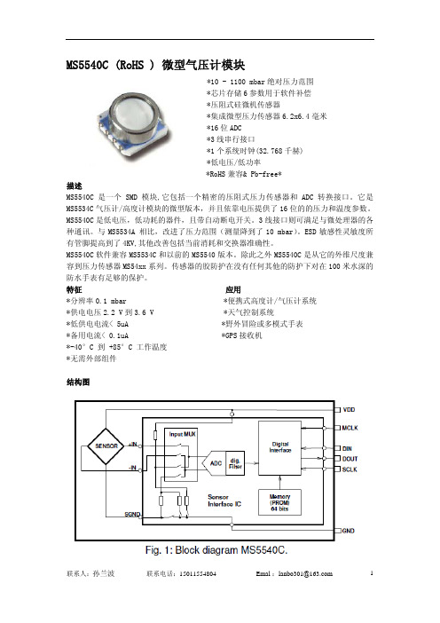
压力和温度测量
压力和温度读数次序和软件补偿操作在图3,图5的流程图里有描述。 首先通过串行接口读取1段字节到4段字节。重起连接MS5540C串行接口的微控制器后可以立 即完成1段字节到4段字节的读取。 其次补偿系数C1到C6通过逻辑和转移操作逐位提取(参见 图4). 为压力测量微控制器在闭路环内(例如每秒钟)必须通过串行接口为压力(D1)和温度(D2) 读 16个位值。然后,根据图3的运算法则,补偿的压力在D1、D2和C1至C6外面被计算(根据图5, 可能使用二次方温度补偿).增殖的结果也许是由32位长决定(+sign)。 在流程中根据图3每 次增殖伴随一次分裂。 这次分裂可以通过逐位转移执行(到功率2是除数)。可以保证的是这 些分裂的结果少于65536(16位)。 由于信号定时由1段字节到4段字节,D1和 D2读出,请参见“串行接口”章节
联系人:孙兰波
联系电话:15011554804
Emal :lanbo301@
9
Fig. 3:压力/温度读取和软件补偿流程图
注意
1)可以不连续地读取D2,但在这种情况下结果将是较为不稳定的。 2)为0.1mbar分辨率显示的稳定性,建议显示8其后的压力平均值。
联系人:孙兰波
联系电话:15011554804
*-40°C 到 +85°C 工作温度
*无需外部组件
结构图
联系人:孙兰波
联系电话:15011554804
Emal :lanbo301@
SOCAY瞬变二极管SMAJ54C型号

SOCAY瞬变二极管SMAJ54C型号
硕凯电子(Sylvia)
一、产品图
1、为表面安装应用优化电路板空间
2、低泄漏
3、单向单元
4、玻璃钝化结
5、低电感
6、优良的钳位能力
7、400W的峰值功率能力在10×1000μ波形重复率(占空比):0.01%
8、快速响应时间:从0伏特到最小击穿电压通常小于1.0ps
9、典型的,在电压高于12V时,反向漏电流小于5μA
10、高温焊接:终端260°C/40秒
11、典型的最大温度系数△Vbr=0.1%x Vbr@25°C x△T
12、塑料包装有保险商实验室可燃性94V-0
13、无铅镀雾锡
14、无卤化,符合RoHS
15、典型失效模式是在指定的电压或电流下出现
16、晶须测试是基于JEDEC JESD201A每个表4a及4c进行的
17、IEC-61000-4-2ESD15kV(空气),8kV(接触)
18、数据线的ESD保护符合IEC61000-4-2(IEC801-2)
19、数据线的EFT保护符合IEC61000-4-4(IEC801-4)
三、应用范围
TVS器件非常适合保护I/O接口,Vcc总线和其他应用于电信、计算机、工业和消费电子应用的易损电路。
五、UL认证编号
六、特性曲线
七、产品尺寸。
MEMORY存储芯片TJA1145T_FDJ中文规格书

1.General descriptionThe TJA1145 is a high-speed CAN transceiver that provides an interface between aController Area Network (CAN) protocol controller and the physical two-wire CAN bus.The transceiver is designed for high-speed CAN applications in the automotive industry,providing differential transmit and receive capability to (a microcontroller with) a CANprotocol controller.The TJA1145 features very low power consumption in Standby and Sleep modes andsupports ISO 11898-2:2016 compliant CAN Partial Networking by means of a selectivewake-up function.A dedicated implementation of the partial networking function has been embedded intothe TJA1145/FD variants TJA1145T/FD and TJA1145TK/FD (see Section7.3.2 for furtherdetails on CAN FD). This function is called ‘FD-passive’ and is the ability to ignore CANFD frames while waiting for a valid wake-up frame in Sleep/Standby mode. This additionalfeature of partial networking is the perfect fit for networks that support both CAN FD andstandard CAN 2.0 communications. It allows normal CAN controllers that do not need tocommunicate CAN FD messages to remain in partial networking Sleep/Standby modeduring CAN FD communication without generating bus errors.Advanced power management regulates the supply throughout the node and supportslocal and remote wake-up functionality. I/O levels are automatically adjusted to the I/Olevels of the controller, allowing the TJA1145 to interface directly with 3.3 V to 5 Vmicrocontrollers. An SPI interface is provided for transceiver control and for retrievingstatus information. Bus connections are truly floating when power is off.The TJA1145 implements the CAN physical layer as defined in ISO 11898-2:2016 andSAE J2284-1 to SAE J2284-4. This implementation enables reliable communication in theCAN FD fast phase at data rates up to 2 Mbit/s.These features make the TJA1145 the ideal choice for high-speed CAN networkscontaining nodes that are always connected to the battery supply line but, in order tominimize current consumption, are only active when required by the application.2.Features and benefits2.1General⏹ISO 11898-2:2016 and SAE J2284-1 to SAE J2284-4 compliant⏹Timing guaranteed for data rates up to 2Mbit/s⏹Autonomous bus biasing according to ISO 11898-2:2016⏹Optimized for in-vehicle high-speed CAN communication⏹No ‘false’ wake-ups due to CAN FD in TJA1145/FD variantsNXP Semiconductors TJA1145High-speed CAN transceiver for partial networking2.2Designed for automotive applications⏹±8 kV ElectroStatic Discharge (ESD) protection, according to the Human Body Model(HBM) on the CAN bus pins⏹±6 kV ESD protection, according to IEC 61000-4-2 on pins BAT and WAKE and on theCAN bus pins⏹CAN bus pins short-circuit proof to ±58 V⏹Battery and CAN bus pins protected against transients according to ISO7637-3, testpulses 1, 2a, 3a and 3b.⏹Suitable for use in 12 V and 24 V systems⏹Available in SO14 and leadless HVSON14 package (3 mm ⨯ 4.5 mm) with improvedAutomated Optical Inspection (AOI) capability⏹AEC-Q100 qualified⏹Dark green product (halogen free and Restriction of Hazardous Substances (RoHS)compliant)3.Quick reference dataTable 1.Quick reference dataSymbol Parameter Conditions Min Typ Max Unit V BAT battery supply voltage 4.5-28VV CC supply voltage 4.5- 5.5VV IO supply voltage on pin V IO 2.85- 5.5VV BAT falling 2.8-3V V th(det)poff power-off detection thresholdvoltage4.5- 4.75V V uvd(VCC)undervoltage detection voltageon pin VCCV uvd(VIO)undervoltage detection voltageV BAT >4.5V 2.7- 2.85V on pin VIOI BAT battery supply current Normal mode-1 1.5mA-4059μASleep mode; CAN Offline mode;-40︒C < T vj<85︒C; V BAT = 7V to 18V-4468μAStandby mode; CAN Offline mode;-40︒C < T vj<85︒C; V BAT = 7V to 18VI CC supply current CAN Active mode; CAN recessive; V TXD=V IO-36mACAN Active mode; CAN dominant; V TXD=0V-4565mA- 4.78.5μAStandby/Normal mode; CAN inactive;-40︒C < T vj<85︒CSleep mode; CAN inactive; -40︒C < T vj<85︒C- 3.87μA I IO supply current on pin V IO Standby/Normal mode; -40︒C < T vj<85︒C-7.111μASleep mode; -40︒C < T vj<85︒C-58μA V ESD electrostatic discharge voltage IEC 61000-4-2 on pins CANH, CANL-6-+6kV V CANH voltage on pin CANH-58-+58VV CANL voltage on pin CANL-58-+58VT vj virtual junction temperature-40-+150︒C4.Ordering information5.Block diagramTable 2.Ordering informationType numberPackage NameDescriptionVersion TJA1145T SO14plastic small outline package; 14leads; body width 3.9mm SOT108-1TJA1145T/FD SO14plastic small outline package; 14leads; body width 3.9mm SOT108-1TJA1145TK HVSON14plastic thermal enhanced very thin small outline package; no leads;14terminals; body 3 ⨯ 4.5 ⨯ 0.85 mmSOT1086-2TJA1145TK/FDHVSON14plastic thermal enhanced very thin small outline package; no leads; 14terminals; body 3 ⨯ 4.5 ⨯ 0.85 mmSOT1086-26.Pinning information6.1Pinning6.2Pin descriptionTable 3.Pin descriptionSymbol Pin DescriptionTXD1transmit data inputGND2[1]groundVCC3 5 V CAN transceiver supply voltageRXD4receive data output; reads out data from the bus linesVIO5supply voltage for I/O level adaptorSDO6SPI data outputINH7inhibit output for switching external voltage regulatorsSCK8SPI clock inputWAKE9local wake-up inputBAT10battery supply voltageSDI11SPI data inputCANL12LOW-level CAN bus lineCANH13HIGH-level CAN bus lineSCSN14SPI chip select input[1]HVSON14 package die supply ground is connected to both the GND pin and the exposed center pad. TheGND pin must be soldered to board ground. For enhanced thermal and electrical performance, it isrecommended that the exposed center pad also be soldered to board ground。
SMF15C中文资料

SMF05C, SMF12C, SMF15C,SMF24C5−Line Transient Voltage Suppressor ArrayThis 5−line voltage transient suppressor array is designed for application requiring transient voltage protection capability. It is intended for use in over−transient voltage and ESD sensitive equipment such as computers, printers, automotive electronics,networking communication and other applications. This device features a monolithic common anode design which protects five independent lines in a single SC−88 package.Features•Protects up to 5−Line in a Single SC−88 Package•Peak Power Dissipation − 100 W (8 x 20 m s Waveform)•ESD Rating of Class 3B (Exceeding 8 kV) per Human Body Model and Class C (Exceeding 400 V) per Machine Model.•Compliance with IEC 61000−4−2 (ESD) 15 kV (Air), 8 kV (Contact)•Flammability Rating of UL 94 V−0•Pb−Free Package is Available Applications•Hand−Held Portable Applications •Networking and Telecom •Automotive Electronics •Serial and Parallel Ports•Notebooks, Desktops, ServersMAXIMUM RATINGS (T J =25°C unless otherwise specified)Maximum ratings are those values beyond which device damage can occur.Maximum ratings applied to the device are individual stress limit values (not normal operating conditions) and are not valid simultaneously. If these limits are exceeded, device functional operation is not implied, damage may occur and reliability may be affected.1.Nonrepetitive current pulse per Figure 3.DevicePackage Shipping †ORDERING INFORMATIONSMF05CT1SC−883000/T ape & Reel SMF12CT1SC−883000/T ape & Reel SMF15CT1SC−883000/T ape & Reel SMF24CT1SC−883000/T ape & Reel†For information on tape and reel specifications,including part orientation and tape sizes, please refer to our Tape and Reel Packaging Specification Brochure, BRD8011/D.*The “T2” suffix refers to an alternate tape & reel orientation.SMF05CT2*SC−883000/T ape & Reel SMF05CT2G*SC−88(Pb−Free)3000/T ape & ReelSMF05C ELECTRICAL CHARACTERISTICS (T J = 25°C unless otherwise specified)SMF12C ELECTRICAL CHARACTERISTICS (T J = 25°C unless otherwise specified)SMF15C ELECTRICAL CHARACTERISTICS (T = 25°C, unless otherwise specified)SMF24C ELECTRICAL CHARACTERISTICS (T = 25°C, unless otherwise specified)S devices are normally selected according to the working peak reverse voltage (V RWM), which should be equal or greater than the DCor continuous peak operating voltage level.3.V BR is measured at pulse test current I T.TYPICAL PERFORMANCE CURVES(T J = 25°C unless otherwise specified)Figure 1. Pulse Derating Curve10090807060504030201000255075100125175200T A , AMBIENT TEMPERATURE (°C)Figure 2. 8 × 20 m s Pulse Waveform1009080706050403020100t, TIME (m s)% O F P E A K P U L S E C U R R E N TFigure 3. Clamping Voltage vs Peak Pulse Current 100101I PP , PEAK PULSE CURRENT (A)V C L A M P , C L A M P I N G V O L T A G E (V )Figure 4. Junction Capacitance vs Reverse VoltageV BR , REVERSE VOLTAGE (V)P E A K P O W E R D I S S I P A T I O N (%)PACKAGE DIMENSIONSSTYLE 24:PIN 1.CATHODE2.ANODE3.CATHODE4.CATHODE5.CATHODE6.CATHODENOTES:1.DIMENSIONING AND TOLERANCING PER ANSI Y14.5M, 1982.2.CONTROLLING DIMENSION: INCH.3.419B−01 OBSOLETE, NEW STANDARD 419B−02.DIM A MIN MAX MIN MAX MILLIMETERS 1.80 2.200.0710.087INCHES B 1.15 1.350.0450.053C 0.80 1.100.0310.043D 0.100.300.0040.012G 0.65 BSC 0.026 BSC H −−−0.10−−−0.004J 0.100.250.0040.010K 0.100.300.0040.012N 0.20 REF 0.008 REF S2.00 2.200.0790.087SC−88/SC70−6/SOT−363CASE 419B−02ISSUE 02U*For additional information on our Pb−Free strategy and solderingdetails, please download the ON Semiconductor Soldering and Mounting Techniques Reference Manual, SOLDERRM/D.SOLDERING FOOTPRINT*ON Semiconductor and are registered trademarks of Semiconductor Components Industries, LLC (SCILLC). SCILLC reserves the right to make changes without further notice to any products herein. SCILLC makes no warranty, representation or guarantee regarding the suitability of its products for any particular purpose, nor does SCILLC assume any liability arising out of the application or use of any product or circuit, and specifically disclaims any and all liability, including without limitation special, consequential or incidental damages.“Typical” parameters which may be provided in SCILLC data sheets and/or specifications can and do vary in different applications and actual performance may vary over time. All operating parameters, including “Typicals” must be validated for each customer application by customer’s technical experts. SCILLC does not convey any license under its patent rights nor the rights of others. SCILLC products are not designed, intended, or authorized for use as components in systems intended for surgical implant into the body, or other applications intended to support or sustain life, or for any other application in which the failure of the SCILLC product could create a situation where personal injury or death may occur. Should Buyer purchase or use SCILLC products for any such unintended or unauthorized application, Buyer shall indemnify and hold SCILLC and its officers, employees, subsidiaries, affiliates,and distributors harmless against all claims, costs, damages, and expenses, and reasonable attorney fees arising out of, directly or indirectly, any claim of personal injury or death associated with such unintended or unauthorized use, even if such claim alleges that SCILLC was negligent regarding the design or manufacture of the part. SCILLC is an Equal Opportunity/Affirmative Action Employer. This literature is subject to all applicable copyright laws and is not for resale in any manner.PUBLICATION ORDERING INFORMATION。
ADuM7701 16位隔离式∑-

Rev. 0 Document Feedback Information furnished by Analog Devices is believed to be accurate and reliable.However,no responsibility is assumed by Analog Devices for its use, nor for any infringements of patents or other rights of third parties that may result from its use. Specifications subject to change without notice. No license is granted by implication or otherwise under any patent or patent rights of Analog Devices. Trademarks and registered trademarks are the property of their respective owners. One Technology Way, P.O. Box 9106, Norwood, M A 02062-9106, U.S.A. Tel: 781.329.4700 ©2019 Analog Devices, Inc. All rights reserved. Technical Support /cn16位隔离式∑-∆调制器数据手册ADuM7701产品特性主机时钟输入频率:5 MHz至21 MHz失调漂移与温度的关系:±0.6 μV/°C(最大值)SNR:86 dB(典型值)16位无失码满量程模拟输入电压范围:±320 mVENOB:14位(典型值)I DD1:10 mA(最大值)板载数字隔离器工作温度范围:−40°C至+125°C高共模瞬变抗扰度:150 kV/μs(最小值),V DD2 = 3.3 V 宽体SOIC16引脚SOIC_W8引脚SOIC_IC封装,支持更高的爬电距离安全和监管批准(申请中)UL认证1分钟5700 V rms,符合UL 1577标准CSA元件验收通知5A符合VDE标准证书DIN V VDE V 0884-10:V IORM = 1270 V PEAKDIN V VDE V 0884-11:V IORM = 1060 V PEAK应用分路电流监控交流电机控制功率和太阳能逆变器风力涡轮机逆变器模数及光耦的替代方案功能框图图1.概述ADuM7701是一款高性能二阶Σ-Δ调制器,片内的数字隔离采用ADI公司的iCoupler®技术,能将模拟输入信号转换为高速单位数据流。
MEMORY存储芯片TJA1145T_FDJ中文规格书
1.General descriptionThe TJA1145 is a high-speed CAN transceiver that provides an interface between aController Area Network (CAN) protocol controller and the physical two-wire CAN bus.The transceiver is designed for high-speed CAN applications in the automotive industry,providing differential transmit and receive capability to (a microcontroller with) a CANprotocol controller.The TJA1145 features very low power consumption in Standby and Sleep modes andsupports ISO 11898-2:2016 compliant CAN Partial Networking by means of a selectivewake-up function.A dedicated implementation of the partial networking function has been embedded intothe TJA1145/FD variants TJA1145T/FD and TJA1145TK/FD (see Section7.3.2 for furtherdetails on CAN FD). This function is called ‘FD-passive’ and is the ability to ignore CANFD frames while waiting for a valid wake-up frame in Sleep/Standby mode. This additionalfeature of partial networking is the perfect fit for networks that support both CAN FD andstandard CAN 2.0 communications. It allows normal CAN controllers that do not need tocommunicate CAN FD messages to remain in partial networking Sleep/Standby modeduring CAN FD communication without generating bus errors.Advanced power management regulates the supply throughout the node and supportslocal and remote wake-up functionality. I/O levels are automatically adjusted to the I/Olevels of the controller, allowing the TJA1145 to interface directly with 3.3 V to 5 Vmicrocontrollers. An SPI interface is provided for transceiver control and for retrievingstatus information. Bus connections are truly floating when power is off.The TJA1145 implements the CAN physical layer as defined in ISO 11898-2:2016 andSAE J2284-1 to SAE J2284-4. This implementation enables reliable communication in theCAN FD fast phase at data rates up to 2 Mbit/s.These features make the TJA1145 the ideal choice for high-speed CAN networkscontaining nodes that are always connected to the battery supply line but, in order tominimize current consumption, are only active when required by the application.2.Features and benefits2.1General⏹ISO 11898-2:2016 and SAE J2284-1 to SAE J2284-4 compliant⏹Timing guaranteed for data rates up to 2Mbit/s⏹Autonomous bus biasing according to ISO 11898-2:2016⏹Optimized for in-vehicle high-speed CAN communication⏹No ‘false’ wake-ups due to CAN FD in TJA1145/FD variantsNXP Semiconductors TJA1145High-speed CAN transceiver for partial networking2.2Designed for automotive applications⏹±8 kV ElectroStatic Discharge (ESD) protection, according to the Human Body Model(HBM) on the CAN bus pins⏹±6 kV ESD protection, according to IEC 61000-4-2 on pins BAT and WAKE and on theCAN bus pins⏹CAN bus pins short-circuit proof to ±58 V⏹Battery and CAN bus pins protected against transients according to ISO7637-3, testpulses 1, 2a, 3a and 3b.⏹Suitable for use in 12 V and 24 V systems⏹Available in SO14 and leadless HVSON14 package (3 mm ⨯ 4.5 mm) with improvedAutomated Optical Inspection (AOI) capability⏹AEC-Q100 qualified⏹Dark green product (halogen free and Restriction of Hazardous Substances (RoHS)compliant)3.Quick reference dataTable 1.Quick reference dataSymbol Parameter Conditions Min Typ Max Unit V BAT battery supply voltage 4.5-28VV CC supply voltage 4.5- 5.5VV IO supply voltage on pin V IO 2.85- 5.5VV BAT falling 2.8-3V V th(det)poff power-off detection thresholdvoltage4.5- 4.75V V uvd(VCC)undervoltage detection voltageon pin VCCV uvd(VIO)undervoltage detection voltageV BAT >4.5V 2.7- 2.85V on pin VIOI BAT battery supply current Normal mode-1 1.5mA-4059μASleep mode; CAN Offline mode;-40︒C < T vj<85︒C; V BAT = 7V to 18V-4468μAStandby mode; CAN Offline mode;-40︒C < T vj<85︒C; V BAT = 7V to 18VI CC supply current CAN Active mode; CAN recessive; V TXD=V IO-36mACAN Active mode; CAN dominant; V TXD=0V-4565mA- 4.78.5μAStandby/Normal mode; CAN inactive;-40︒C < T vj<85︒CSleep mode; CAN inactive; -40︒C < T vj<85︒C- 3.87μA I IO supply current on pin V IO Standby/Normal mode; -40︒C < T vj<85︒C-7.111μASleep mode; -40︒C < T vj<85︒C-58μA V ESD electrostatic discharge voltage IEC 61000-4-2 on pins CANH, CANL-6-+6kV V CANH voltage on pin CANH-58-+58VV CANL voltage on pin CANL-58-+58VT vj virtual junction temperature-40-+150︒C4.Ordering information5.Block diagramTable 2.Ordering informationType numberPackage NameDescriptionVersion TJA1145T SO14plastic small outline package; 14leads; body width 3.9mm SOT108-1TJA1145T/FD SO14plastic small outline package; 14leads; body width 3.9mm SOT108-1TJA1145TK HVSON14plastic thermal enhanced very thin small outline package; no leads;14terminals; body 3 ⨯ 4.5 ⨯ 0.85 mmSOT1086-2TJA1145TK/FDHVSON14plastic thermal enhanced very thin small outline package; no leads; 14terminals; body 3 ⨯ 4.5 ⨯ 0.85 mmSOT1086-26.Pinning information6.1Pinning6.2Pin descriptionTable 3.Pin descriptionSymbol Pin DescriptionTXD1transmit data inputGND2[1]groundVCC3 5 V CAN transceiver supply voltageRXD4receive data output; reads out data from the bus linesVIO5supply voltage for I/O level adaptorSDO6SPI data outputINH7inhibit output for switching external voltage regulatorsSCK8SPI clock inputWAKE9local wake-up inputBAT10battery supply voltageSDI11SPI data inputCANL12LOW-level CAN bus lineCANH13HIGH-level CAN bus lineSCSN14SPI chip select input[1]HVSON14 package die supply ground is connected to both the GND pin and the exposed center pad. TheGND pin must be soldered to board ground. For enhanced thermal and electrical performance, it isrecommended that the exposed center pad also be soldered to board ground。
- 1、下载文档前请自行甄别文档内容的完整性,平台不提供额外的编辑、内容补充、找答案等附加服务。
- 2、"仅部分预览"的文档,不可在线预览部分如存在完整性等问题,可反馈申请退款(可完整预览的文档不适用该条件!)。
- 3、如文档侵犯您的权益,请联系客服反馈,我们会尽快为您处理(人工客服工作时间:9:00-18:30)。
SM1100C SERIES
n CMOS COMPATIBLE WITH TRI−STATE OUTPUT
n SURFACE MOUNT OSCILLATORS IN PLASTIC PACKAGE
n LAND PATTERN COMPATIBLE TO OUR ENTIRE SM1100X SERIES AND EPSON SG615
STANDARD SPECIFICATIONS:
Frequency Range 1.000 MHz – 50.000 MHz (Consult factory for specific available frequencies) Frequency Stability over Operating
Temperature Range
± 50 PPM is standard, but ± 25 PPM is also available for certain frequencies.
Operating Temperature Range 0 - 70°C is standard, but can be extended to −40 to +85°C for
certain frequencies
1.000 MHz – 30.000 MHz 30.001 MHz – 50.000 MHz
SM1100CY SM1100CY SM1100CV
Operable Supply Voltage (Vcc)
5 Volt ± 10% or 3.3 Volt ± 10% 5 Volt ± 10% only 3.3 Volt ± 10% only
Symmetry (Duty Cycle) (See next page for definition.) 40/60 - 60/40% is standard, but 45/55% symmetry at 50% of Vcc is also available.
Input Current (Icc) & Rise and Fall Time
(Tr & Tf) & Jitter
Depends on frequency and output load. See next page. Logic “1” & Logic “0” (See next page) 90% of Vcc MIN.; 10% of Vcc MAX.
Output Load 15 pF is standard. Contact factory for heavier loads.
Tri-state Output Normal output when pin #1 is open (no connection); Normal output when pin #1 is at logic “1”;
High-Impedance Output when pin #1 is at logic “0”.
Packaging (see page R1, Figure 2) 24 mm tape, 330 mm reel: 1000 parts per reel. For quantities <250: 23 parts per tube.
PART NUMBERING GUIDE:
n The Pletronics part number for an SM1100C series oscillator consists of the following 3 elements:
1. Overall Frequency Stability over Operating Temperature Range:
SM1145C: ± 50 PPM;
SM1144C: ± 25 PPM
2. Optional Alphabet Designator for Special Requirement:
SM1100CY: standard specifications;
SM1145CE: operating temperature range of -40 to +85°C;
SM1100CS: 45/55% symmetry at 50% of Vcc;
SM1100CV: operates at Vcc = 3.3V (only needed for over 30.000MHz)
(There are other alphabet designators not listed here.)
3. Frequency of Operation in MHz
EXAMPLES: SM1145CV-50.000 MHz; SM1145CS-10.000 MHz; SM1144CE-50.000 MHz
n When customer’s requirements are non-standard, a special engineering part number will be assigned.
(continued)
Telephone: (425) 776-1880, Fax: (425) 776-2760, e-mail: ple-sales@ O7A
O7B
Pletronics Inc., 19013 36th Ave. W., Suite H, Lynnwood, WA 98036-5761 USA
SM1100C SERIES
Input Current (Icc), Rise and Fall time with 15pF Load & Jitter
Icc (mA) Tr & Tf (nS) Period Jitter RMS Values
(pS: 1 x 10-12 Sec) Frequency Range
(MHz) Typical Maximum Typical Maximum
Typical Maximum 1.000 – 7.999 5.0 10.0 5.5 6.5 30.0 50.0 8.000 – 23.999 8.0 15.0 5.5 6.5 30.0 50.0 24.000 – 29.999 10.0 15.0 4.5 5.5 20.0 30.0 30.000 – 50.000
25.0
30.0
2.5
3.5
15.0 25.0
Waveform
Recommended Test Circuit with CMOS Load
* CL (Capacitive Load): Includes the input capacitance of oscilloscope.
** 0.01µF external by-pass filter is recommended.
Package Outline (NOT TO SCALE):
January 2000
PIN CONNECTIONS
PIN CONNECTION
1 2 3 4
ENABLE/DISABLE INPUT GROUND OUTPUT Vcc
INCHES (MILLIMETERS)。