PAM8610TR中文资料
英国深海控制器 DSE8610调试人员专用说明
DSE8610 操作说明书
(内部资料)
深圳海汇科技有限公司
深圳市南山区南山大道2002号光彩新天地大厦8B1-8B2 电话:0755 2646 6606 传真:0755 2646 6609
深圳海汇科技有限公司
目录
章节
页数
1 控制器界面........................................................................................................3 2 按键...................................................................................................................3 3 LED 指示灯 .......................................................................................................4 4 选择模式 ...........................................................................................................5 5 操作模式 ...........................................................................................................5 6 浏览/查看控制器测量的各种参数.......................................................................6 7 排除故障 ...........................................................................................................8 8 控制器参数设置方法 .........................................................................................9
LMV861MG资料

February 22, 2008 LMV861/LMV86230 MHz Low Power CMOS, EMI Hardened Operational AmplifiersGeneral DescriptionNational’s LMV861 and LMV862 are CMOS input, low power op amp IC's, providing a low input bias current, a wide tem-perature range of −40°C to +125°C and exceptional perfor-mance making them robust general purpose parts. Addition-ally, the LMV861 and LMV862 are EMI hardened to minimize any interference so they are ideal for EMI sensitive applica-tions.The unity gain stable LMV861 and LMV862 feature 30 MHz of bandwidth while consuming only 2.25 mA of current per channel. These parts also maintain stability for capacitive loads as large as 200 pF. The LMV861 and LMV862 provide superior performance and economy in terms of power and space usage.This family of parts has a maximum input offset voltage of 1 mV, a rail-to-rail output stage and an input common-mode voltage range that includes ground. Over an operating range from 2.7V to 5.5V the LMV861 and LMV862 provide a PSRR of 93 dB, and a CMRR of 93 dB. The LMV861 is offered in the space saving 5-Pin SC70 package, and the LMV862 in the 8-Pin MSOP.FeaturesUnless otherwise noted, typical values at TA= 25°C, V+ = 3.3V■Supply voltage 2.7V to 5.5V ■Supply current (per channel) 2.25 mA ■Input offset voltage 1 mV max ■Input bias current0.1 pA ■GBW30 MHz ■EMIRR at 1.8 GHz105 dB ■Input noise voltage at 1 kHz8 nV/√Hz ■Slew rate18 V/µs ■Output voltage swing Rail-to-Rail ■Output current drive67 mA ■Operating ambient temperature range−40°C to 125°C Applications■Photodiode preamp■Weight scale systems■Filters/buffers■Medical diagnosis equipmentTypical ApplicationEMI Hardened Sensor Application30024001© 2008 National Semiconductor LMV861 Single/ LMV862 Dual 30 MHz Low Power CMOS, EMI Hardened Operational AmplifiersAbsolute Maximum Ratings (Note 1)If Military/Aerospace specified devices are required,please contact the National Semiconductor Sales Office/Distributors for availability and specifications.ESD Tolerance (Note 2) Human Body Model 2 kV Charge-Device Model 1 kV Machine Model 200VV IN Differential± Supply VoltageSupply Voltage (V + – V −)6V Voltage at Input/Output PinsV + +0.4V V − −0.4VStorage Temperature Range −65°C to +150°CJunction Temperature (Note 3)+150°CSoldering InformationInfrared or Convection (20 sec)260°COperating Ratings(Note 1)Temperature Range (Note 3)−40°C to +125°CSupply Voltage (V + – V −)2.7V to 5.5VPackage Thermal Resistance (θJA (Note 3)) 5-Pin SC70302°C/W 8-Pin MSOP217°C/W3.3V Electrical Characteristics(Note 4)Unless otherwise specified, all limits are guaranteed for T A = 25°C, V + = 3.3V, V − = 0V, V CM = V +/2, and R L =10 k Ω to V +/2.Boldface limits apply at the temperature extremes.Symbol ParameterConditionsMin (Note 6)Typ (Note 5)Max (Note 6)UnitsV OS Input Offset Voltage (Note 9)±273±10001260μV TCV OS Input Offset Voltage Drift (Notes 9, 10) ±0.7±2.6μV/°C I B Input Bias Current (Note 10)0.110500pA I OS Input Offset Current1 pA CMRR Common Mode Rejection Ratio (Note 9)0.2V ≤ V CM ≤ V + - 1.2V 777593 dB PSRR Power Supply Rejection Ratio (Note 9)2.7V ≤ V + ≤ 5.5V,V OUT = 1V777693 dBEMIRREMI Rejection Ratio, IN+ and IN−(Note 8)V RF_PEAK = 100 mV P (−20 dBV P ),f = 400 MHz70 dB V RF_PEAK = 100 mV P (−20 dBV P ),f = 900 MHz80 V RF_PEAK = 100 mV P (−20 dBV P ),f = 1800 MHz105 V RF_PEAK = 100 mV P (−20 dBV P ),f = 2400 MHz110 CMVR Input Common-Mode Voltage Range CMRR ≥ 65 dB −0.1 2.1V A VOLLarge Signal Voltage Gain (Note 11)R L = 2 k ΩV OUT = 0.15V to 1.65V,V OUT = 3.15V to 1.65V 10097110dBR L = 10 k ΩV OUT = 0.1V to 1.65V,V OUT = 3.2V to 1.65V10098113V OOutput Swing High,(measured from V +)R L = 2 k Ω to V +/2 121418mVR L = 10 k Ω to V +/2345Output Swing Low,(measured from V −)R L = 2 k Ω to V +/2 81216mVR L = 10 k Ω to V +/2245 2L M V 861 S i n g l e / L M V 862 D u a lSymbol Parameter Conditions Min(Note 6)Typ(Note 5)Max(Note 6)UnitsI O Output Short Circuit Current Sourcing, VOUT= VCM,VIN= 100 mV615270mASinking, VOUT= VCM,VIN= −100 mV725886ISSupply Current LMV861 2.25 2.593.00mALMV862 4.4SR Slew Rate (Note 7)AV = +1, VOUT= 1 VPP,10% to 90%18V/μs GBW Gain Bandwidth Product30MHz Φm Phase Margin70dege n Input-Referred Voltage Noisef = 1 kHz8nV/f = 100 kHz5inInput-Referred Current Noise f = 1 kHz0.015pA/ROUTClosed Loop Output Impedance f = 20 MHz80ΩC IN Common-Mode Input Capacitance21pF Differential-Mode Input Capacitance15THD Total Harmonic Distortion f = 1 kHz, AV= 1, BW ≥ 500 kHz0.02% 5V Electrical Characteristics (Note 4)Unless otherwise specified, all limits are guaranteed for T = 25°C, V+ = 5V, V− = 0V, VCM = V+/2, and RL=10 kΩ to V+/2. Bold-face limits apply at the temperature extremes.Symbol Parameter Conditions Min(Note 6)Typ(Note 5)Max(Note 6)UnitsVOSInput Offset Voltage(Note 9)±273±10001260μVTCVOSInput Offset Voltage Drift(Notes 9, 10)±0.7±2.6μV/°CIBInput Bias Current(Note 10)0.110500pAIOSInput Offset Current1pACMRR Common-Mode Rejection Ratio(Note 9)0V ≤ V CM ≤ V+ –1.2V787794dBPSRR Power Supply Rejection Ratio(Note 9)2.7V ≤ V+≤ 5.5V,VOUT= 1V777693dBEMIRR EMI Rejection Ratio, IN+ and IN−(Note 8)VRF_PEAK= 100 mVP(−20 dBVP),f = 400 MHz70dB VRF_PEAK= 100 mVP(−20 dBVP),f = 900 MHz80VRF_PEAK= 100 mVP(−20 dBVP),f = 1800 MHz105VRF_PEAK= 100 mVP(−20 dBVP),f = 2400 MHz110CMVR Input Common-Mode Voltage Range CMRR ≥ 65 dB−0.1 3.9VAVOLLarge Signal Voltage Gain(Note 11)RL= 2 kΩVOUT= 0.15V to 2.5V,VOUT= 4.85V to 2.5V103100111dBRL= 10 kΩVOUT= 0.1V to 2.5V,VOUT= 4.9V to 2.5V103100113LMV861 Single/ LMV862 DualSymbol ParameterConditionsMin (Note 6)Typ (Note 5)Max (Note 6)UnitsV OOutput Swing High,(measured from V +)R L = 2 k Ω to V +/2 131519mVR L = 10 k Ω to V +/2345Output Swing Low,(measured from V −)R L = 2 k Ω to V +/2 101418mVR L = 10 k Ω to V +/2345I OOutput Short Circuit CurrentSourcing, V OUT = V CM ,V IN = 100 mV 9086150 mA Sinking, V OUT = V CM ,V IN = −100 mV9086150 I SSupply CurrentLMV861 2.47 2.843.27mALMV8624.9 SR Slew Rate (Note 7)A V = +1, V OUT = 2V PP ,10% to 90%20 V/μs GBW Gain Bandwidth Product31 MHz Φm Phase Margin71 deg e n Input-Referred Voltage Noise f = 1 kHz 8 nV/f = 100 kHz 5 i n Input-Referred Current Noise f = 1 kHz0.015 pA/R OUT Closed Loop Output Impedance f = 20 MHz 60 ΩC IN Common-Mode Input Capacitance 20 pF Differential-Mode Input Capacitance15 THDTotal Harmonic Distortionf = 1 kHz, A V = 1, BW ≥ 500 kHz0.02%Note 1:Absolute Maximum Ratings indicate limits beyond which damage to the device may occur. Operating Ratings indicate conditions for which the device is intended to be functional, but specific performance is not guaranteed. For guaranteed specifications and the test conditions, see the Electrical Characteristics Tables.Note 2:Human Body Model, applicable std. MIL-STD-883, Method 3015.7. Machine Model, applicable std. JESD22-A115-A (ESD MM std. of JEDEC) Field-Induced Charge-Device Model, applicable std. JESD22-C101-C (ESD FICDM std. of JEDEC).Note 3:The maximum power dissipation is a function of T J(MAX), θJA , and T A . The maximum allowable power dissipation at any ambient temperature is P D = (T J(MAX) - T A )/ θJA . All numbers apply for packages soldered directly onto a PC board.Note 4:Electrical table values apply only for factory testing conditions at the temperature indicated. Factory testing conditions result in very limited self-heating of the device.Note 5:Typical values represent the most likely parametric norm as determined at the time of characterization. Actual typical values may vary over time and will also depend on the application and configuration. The typical values are not tested and are not guaranteed on shipped production material.Note 6:Limits are 100% production tested at 25°C. Limits over the operating temperature range are guaranteed through correlations using statistical quality control (SQC) method.Note 7:Number specified is the slower of positive and negative slew rates.Note 8:The EMI Rejection Ratio is defined as EMIRR = 20log ( V RF_PEAK /ΔV OS ).Note 9:The typical value is calculated by applying absolute value transform to the distribution, then taking the statistical average of the resulting distribution Note 10:This parameter is guaranteed by design and/or characterization and is not tested in production.Note 11:The specified limits represent the lower of the measured values for each output range condition. 4L M V 861 S i n g l e / L M V 862 D u a lConnection Diagrams5-Pin SC7030024002Top View8-Pin MSOP30024003Top ViewOrdering InformationPackage Part Number Package MarkingTransport Media NSC Drawing Status 5-Pin SC70LMV861MG AEA 1k units Tape and Reel MAA05A Release LMV861MGX 3k units Tape and Reel 8-Pin MSOPLMV862MM AJ5A1k units Tape and Reel MUA08APreliminaryLMV862MMX3.5k units Tape and ReelLMV861 Single/ LMV862 DualTypical Performance CharacteristicsAt T A = 25°C. R L = 10 k Ω, V + = 3.3V, V − = 0V, unless otherwisespecified.V OS vs. V CM at V + = 3.3V30024010V OS vs. V CM at V + = 5.0V30024011V OS vs. Supply Voltage 30024012V OS vs. Temperature30024013V OS vs. V OUT 30024014Input Bias Current vs. V CM at 25°C30024015 6L M V 861 S i n g l e / L M V 862 D u a lInput Bias Current vs. VCMat 85°C30024016Input Bias Current vs. VCMat 125°C30024017Supply Current vs. Supply Voltage Single LMV86130024018Supply Current vs. Supply Voltage Dual LMV86230024019Supply Current vs. Temperature Single LMV86130024021Supply Current vs. Temperature Dual LMV86230024022LMV861 Single/ LMV862 DualSinking Current vs. Supply Voltage30024024Sourcing Current vs. Supply Voltage30024025Output Swing High vs. Supply Voltage R L = 2 k Ω30024026Output Swing High vs. Supply Voltage R L = 10 k Ω30024027Output Swing Low vs. Supply Voltage R L = 2 k Ω30024028Output Swing Low vs. Supply Voltage R L = 10 k Ω30024029 8L M V 861 S i n g l e / L M V 862 D u a lOutput Voltage Swing vs. Load Current at V+ = 3.3V30024030Output Voltage Swing vs. Load Current at V+ = 5.0V30024031Open Loop Frequency Response vs. Temperature30024032Open Loop Frequency Response vs. Load Conditions30024033Phase Margin vs. Capacitive Load30024034PSRR vs. Frequency30024035LMV861 Single/ LMV862 DualCMRR vs. Frequency30024036Channel Separation vs. Frequency30024037Large Signal Step Response with Gain = 130024038Large Signal Step Response with Gain = 1030024039Small Signal Step Response with Gain = 130024040Small Signal Step Response with Gain = 1030024041 10L M V 861 S i n g l e / L M V 862 D u a lSlew Rate vs. Supply Voltage30024042Input Voltage Noise vs. Frequency30024044THD+N vs. Frequency30024045THD+N vs. Amplitude30024046ROUTvs. Frequency30024047EMIRR IN+ vs. Power at 400 MHz30024048LMV861 Single/ LMV862 DualEMIRR IN+ vs. Power at 900 MHz30024049EMIRR IN+ vs. Power at 1800 MHz30024050EMIRR IN+ vs. Power at 2400 MHz 30024051EMIRR IN+ vs. Frequency30024052 12L M V 861 S i n g l e / L M V 862 D u a lApplication InformationINTRODUCTIONThe LMV861 and LMV862 are operational amplifiers with ex-cellent specifications, such as low offset, low noise and a rail-to-rail output. These specifications make the LMV861 and LMV862 great choices for medical and instrumentation appli-cations such as diagnosis equipment and power line moni-tors. The low supply current is perfect for battery powered equipment. The small packages, SC70 package for the LMV861, and the MSOP package for the dual LMV862, make these parts a perfect choice for portable electronics. Addi-tionally, the EMI hardening makes the LMV861 and LMV862a must for almost all op amp applications. Most applications are exposed to Radio Frequency (RF) signals such as the signals transmitted by mobile phones or wireless computer peripherals. The LMV861 and LMV862 will effectively reduce disturbances caused by RF signals to a level that will be hard-ly noticeable. This again reduces the need for additional filtering and shielding. Using this EMI resistant series of op amps will thus reduce the number of components and space needed for applications that are affected by EMI, and will help applications, not yet identified as possible EMI sensitive, to be more robust for EMI.INPUT CHARACTERISTICSThe input common mode voltage range of the LMV861 and LMV862 includes ground, and can even sense well below ground. The CMRR level does not degrade for input levels up to 1.2V below the supply voltage. For a supply voltage of 5V,the maximum voltage that should be applied to the input for best CMRR performance is thus 3.8V.When not configured as unity gain, this input limitation will usually not degrade the effective signal range. The output is rail-to-rail and therefore will introduce no limitations to the signal range.The typical offset is only 0.273 mV, and the TCV OS is 0.7 μV/°C, specifications close to precision op amps.CMRR MEASUREMENTThe CMRR measurement results may need some clarifica-tion. This is because different setups are used to measure the AC CMRR and the DC CMRR.The DC CMRR is derived from ΔV OS versus ΔV CM . This value is stated in the tables, and is tested during production testing.The AC CMRR is measured with the test circuit shown in Figure 1.30024064FIGURE 1. AC CMRR Measurement SetupThe configuration is largely the usually applied balanced con-figuration. With potentiometer P1, the balance can be tuned to compensate for the DC offset in the DUT. The main differ-ence is the addition of the buffer. This buffer prevents the open-loop output impedance of the DUT from affecting the balance of the feedback network. Now the closed-loop output impedance of the buffer is a part of the balance. But as the closed-loop output impedance is much lower, and by careful selection of the buffer also has a larger bandwidth, the total effect is that the CMRR of the DUT can be measured much more accurately. The differences are apparent in the larger measured bandwidth of the AC CMRR.One artifact from this test circuit is that the low frequency CM-RR results appear higher than expected. This is because in the AC CMRR test circuit the potentiometer is used to com-pensate for the DC mismatches. So, mainly AC mismatch is all that remains. Therefore, the obtained DC CMRR from this AC CMRR test circuit tends to be higher than the actual DC CMRR based on DC measurements.The CMRR curve in Figure 2 shows a combination of the AC CMRR and the DC CMRR.30024036FIGURE 2. CMRR CurveLMV861 Single/ LMV862 DualOUTPUT CHARACTERISTICSAs already mentioned the output is rail-to-rail. When loadingthe output with a 10 kΩ resistor the maximum swing of theoutput is typically 3 mV from the positive and negative rail.The output of the LMV861 and LMV862 can drive currents upto 70 mA at 3.3V, and even up to 150 mA at 5V.The LMV861 and LMV862 can be connected as non-invertingunity gain amplifiers. This configuration is the most sensitiveto capacitive loading. The combination of a capacitive loadplaced at the output of an amplifier along with the amplifier’soutput impedance creates a phase lag, which reduces thephase margin of the amplifier. If the phase margin is signifi-cantly reduced, the response will be under damped whichcauses peaking in the transfer and, when there is too muchpeaking, the op amp might start oscillating. The LMV861 andLMV862 can directly drive capacitive loads up to 200 pF with-out any stability issues. In order to drive heavier capacitiveloads, an isolation resistor, RISO, should be used, as shownin Figure 3. By using this isolation resistor, the capacitive loadis isolated from the amplifier’s output, and hence, the polecaused by CLis no longer in the feedback loop. The larger thevalue of RISO, the more stable the amplifier will be. If the valueof RISOis sufficiently large, the feedback loop will be stable,independent of the value of CL. However, larger values ofRISOresult in reduced output swing and reduced output cur-rent drive.30024063FIGURE 3. Isolating Capacitive LoadA resistor value of around 50Ω would be sufficient. As an ex-ample some values are given in the following table, for 5V andan open loop gain of 111 dB.CLOADRISO300 pF62Ω400 pF55Ω500 pF50ΩWhen increasing the closed-loop gain the capacitive load canbe increased even further. With a closed loop gain of 2 and a27Ω isolation resistor, the load can be 1 nFEMIRRWith the increase of RF transmitting devices in the world, theelectromagnetic interference (EMI) between those devicesand other equipment becomes a bigger challenge. TheLMV861 and LMV862 are EMI hardened op amps which arespecifically designed to overcome electromagnetic interfer-ence. Along with EMI hardened op amps, the EMIRR param-eter is introduced to unambiguously specify the EMI perfor-mance of an op amp. This section presents an overview ofEMIRR. A detailed description on this specification for EMIhardened op amps can be found in Application Note AN-1698.The dimensions of an op amp IC are relatively small com-pared to the wavelength of the disturbing RF signals. As aresult the op amp itself will hardly receive any disturbances.The RF signals interfering with the op amp are dominantlyreceived by the PCB and wiring connected to the op amp. Asa result the RF signals on the pins of the op amp can be rep-resented by voltages and currents. This representation sig-nificantly simplifies the unambiguous measurement andspecification of the EMI performance of an op amp.RF signals interfere with op amps via the non-linearity of theop amp circuitry. This non-linearity results in the detection ofthe so called out-of-band signals. The obtained effect is thatthe amplitude modulation of the out-of-band signal is down-converted into the base band. This base band can easilyoverlap with the band of the op amp circuit. As an exampleFigure 4 depicts a typical output signal of a unity-gain con-nected op amp in the presence of an interfering RF signal.Clearly the output voltage varies in the rhythm of the on-offkeying of the RF carrier.30024065FIGURE 4. Offset voltage variation due to an interferingRF signalEMIRR DEFINITIONTo identify EMI hardened op amps, a parameter is neededthat quantitatively describes the EM performance of opamps. A quantitative measure enables the comparison andthe ranking of op amps on their EMI robustness. Thereforethe EMI Rejection Ratio (EMIRR) is introduced. This param-eter describes the resulting input-referred offset voltage shiftof an op amp as a result of an applied RF carrier (interference)with a certain frequency and level. The definition of EMIRR isgiven by:In which VRF_PEAKis the amplitude of the applied un-modu-lated RF signal (V) and ΔVOSis the resulting input-referredoffset voltage shift (V). The offset voltage depends quadrati-cally on the applied RF level, and therefore, the RF level atwhich the EMI RR is determined should be specified. Thestandard level for the RF signal is 100 mVP. Application NoteAN-1698 addresses the conversion of an EMIRR measuredfor an other signal level than 100 mVP. The interpretation ofthe EMIRR parameter is straightforward. When two op ampshave EMIRRs which differ by 20 dB, the resulting error signalswhen used in identical configurations, differs by 20 dB as well.So, the higher the EMIRR, the more robust the op amp.Coupling an RF Signal to the IN+ PinEach of the op amp pins can be tested separately on EMIRR.n this section the measurements on the I N+ pin (which,based on symmetry considerations, also apply to the IN- pin)are discussed. In Application Note AN-1698 the other pins ofthe op amp are treated as well. For testing the IN+ pin the op 14LMV861Single/LMV862Dualamp is connected in the unity gain configuration. Applying the RF signal is straightforward as it can be connected directly to the IN+ pin. As a result the RF signal path has a minimum of components that might affect the RF signal level at the pin. The circuit diagram is shown in Figure 5. The PCB trace fromRFIN to the IN+ pin should be a 50Ω stripline in order to matchthe RF impedance of the cabling and the RF generator. On the PCB a 50Ω termination is used. This 50Ω resistor is also used to set the bias level of the IN+ pin to ground level. For determining the EMIRR, two measurements are needed: one is measuring the DC output level when the RF signal is off; and the other is measuring the DC output level when the RF signal is switched on. The difference of the two DC levels is the output voltage shift as a result of the RF signal. As the op amp is in the unity gain configuration, the input referred offset voltage shift corresponds one-to-one to the measured output voltage shift.30024067 FIGURE 5. Circuit for coupling the RF signal to IN+Cell Phone CallThe effect of electromagnetic interference is demonstrated in a setup where a cell phone interferes with a pressure sensor application. The application is show in Figure 7.This application needs two op amps and therefore a dual op amp is used. The op amp configured as a buffer and con-nected at the negative output of the pressure sensor prevents the loading of the bridge by resistor R2. The buffer also pre-vents the resistors of the sensor from affecting the gain of the following gain stage. The op amps are placed in a single sup-ply configuration.The experiment is performed on two different op amps: a typ-ical standard op amp and the LMV862, EMI hardened dual op amp. A cell phone is placed on a fixed position a couple of centimeters from the op amps in the sensor circuit.When the cell phone is called, the PCB and wiring connected to the op amps receive the RF signal. Subsequently, the op amps detect the RF voltages and currents that end up at their pins. The resulting effect on the output of the second op amp is shown in Figure 6.30024062FIGURE 6. Comparing EMI RobustnessThe difference between the two types of op amps is clearly visible. The typical standard dual op amp has an output shift (disturbed signal) larger than 1V as a result of the RF signal transmitted by the cell phone. The LMV862, EMI hardened op amp does not show any significant disturbances. This means that the RF signal will not disturb the signal entering the ADC when using the LMV862.30024061FIGURE 7. Pressure Sensor Application LMV861 Single/ LMV862 DualDECOUPLING AND LAYOUTCare must be given when creating a board layout for the op amp. For decoupling the supply lines it is suggested that 10 nF capacitors be placed as close as possible to the op amp. For single supply, place a capacitor between V + and V −. For dual supplies, place one capacitor between V + and the board ground, and a second capacitor between ground and V −.Even with the LMV861 and LMV862 inherent hardening against EMI, it is still recommended to keep the input traces short and as far as possible from RF sources. Then the RF signals entering the chip are as low as possible, and the re-maining EMI can be, almost, completely eliminated in the chip by the EMI reducing features of the LMV861 and LMV862.LOAD CELL SENSOR APPLICATIONThe LMV861 and LMV862 can be used for weight measuring system applications which use a load cell sensor. Examples of such systems are: bathroom weight scales, industrial weight scales and weight measurement devices on moving equipment such as forklift trucks.The following example describes a typical load cell sensor application that can be used as a starting point for many dif-ferent types of sensors and applications. Applications in en-vironments where EMI may appear would especially benefit from the EMIRR performance of the LMV861 and LMV862.Load Cell CharacteristicsThe load cell used in this example is a Wheatstone bridge.The value of the resistors in the bridge changes when pres-sure is applied to the sensor. This change of the resistor values will result in a differential output voltage depending on the sensitivity of the sensor, the used supply voltage and the applied pressure. The difference between the output at full scale pressure and the output at zero pressure is defined as the span of the load cell. A typical value for the span is 10 mV/V.The circuit configuration should be chosen such that loading of the sensor is prevented. Loading of the resistor bridge due to the circuit following the sensor, could result in incorrect output voltages of the sensor.Load Cell ExampleFigure 8 shows a typical schematic for a load cell application.It uses a single supply and has an adjustment for both positive and negative offset of the load cell. An ADC converts the am-plified signal to a digital signal.The op amps A1 and A2 are configured as buffers, and are connected at both the positive and the negative output of the load cell. This is to prevent the loading of the resistor bridge in the sensor by the resistors configuring the differential op amp circuit (op amp A4). The buffers also prevent the resis-tors of the sensor from affecting the gain of the following gain stage. The third buffer (A3) is used to create a reference volt-age, to correct for the offset in the system.Given the differential output voltage V S of the load cell, the output signal of this op amp configuration, V OUT , equals:To align the pressure range with the full range of an ADC the correct gain needs to be set. To calculate the correct gain, the power supply voltage and the span of the load cell are need-ed. For this example a power supply of 5V is used and the span of the sensor, in this case a 125 kg sensor, is 100 mV.With the configuration as shown in Figure 8, this signal is covering almost the full input range of the ADC. With no weight on the load cell, the output of the sensor and the op amp A4 will be close to 0V. With the full weight on the load cell, the output of the sensor is 100 mV, and will be amplified with the gain from the configuration. In the case of the con-figuration of Figure 8 the gain is R3 / R1 = 51 k Ω / 100Ω = 50.This will result in a maximum output of 100 mV x 50 = 5V,which covers the full range of the ADC.For further processing the digital signal can be processed by a microprocessor following the ADC, this can be used to dis-play or log the weight on the load cell. To get a resolution of 0.5 kg, the LSB of the ADC should be smaller then 0.5 kg /125 kg = 1/1000. A 12-bit ADC would be sufficient as this gives 4096 steps. A 12-bit ADC such as the two channel 12-bit ADC122S021 can be used for this application.30024069FIGURE 8. Load Cell Application 16L M V 861 S i n g l e / L M V 862 D u a l。
联想手机销售手册
联想手机销售手册Pam168销售手册一、产品理念和定位1、产品理念开放、时尚、个性化〔时尚的外观,目前世界上最轻、最薄的简体中文palmO掌上电脑,引导PDA的时尚潮流;开放式的操作系统提供成千上万的开放式应用软件;不同的用户,不同的应用和设置,造就更趋个性化、得心应手的产品〕轻松工作:超轻、超薄的外观设计,和开放式的PALMO及其应用作为内涵定义,对商务人士演奏出轻松便捷的工作旋律;多彩娱乐型PDA。
MP3和PDA的结合,表达PDA产品的休闲/娱乐应用方向,使更多的用户在更多的时间使用PDA产品。
生活:彩色TFT大屏幕,MP3、录音、电子书、红外短信、PC同步等功能的实现,为消费者引入多彩的视听生活享受;2、产品定位联想Pam168是国内中高端PDA市场中第一款真彩PalmO简体中文手写掌上电脑。
3.目标客户群用户群综合描述:Palm发烧友、外企员工、IT人士、送礼人士;年龄特征:22-45岁;用户核心需求:开放性应用+休闲娱乐+个人助理;典型目标用户:1〕刘先生,24岁,Palm发烧友,对Palm类产品有强烈的偏好;2〕John,某IT职员,熟悉计算机与网络,经常接触其他外企商业人士,对Palm类设备有了解;3〕王小姐,工作繁忙,需要PIM等功能来安排日程、管理时间,喜欢游戏、MP3、电子书等开放式数码应用以求工作之余的放松;4〕小方,需要一个PDA来送礼,但希望自己的PDA有独特之处,媒体和大家的评价是时尚产品;二、产品主要诉求①开放式操作系统②音乐游戏任我行③独有可隐藏“虚拟手写区”④真彩六万五千色TFT显示屏三.销售话术1、销售话述:根据对PALM类产品的认知度,我们把顾客分为两类:一类是普通顾客,一类是PALM发烧友。
针对不同类型顾客,我们介绍产品的话述不同。
〔1〕对普通顾客联想Pam168是国内第一款以PalmO为操作系统的掌上电脑,也是国内第一次引入国际最流行的PDA操作软件的新产品。
TL TR861设置指南

TL TR861设置指南TL-TR861支持中国联通HSPA+制式的3G网络,3G最高下载速率可达21Mbps。
无需接额外的3G上网卡,只需插入中国联通3G标准SIM卡即可将高速的3G网络转化为WIFI信号供平板电脑、智能手机、笔记本电脑等WIFI终端共享3G上网。
下面详细介绍TL-TR861的设置及使用方法。
一、快速设置路由器1.安装SIM卡。
打开路由器后盖,将联通3G卡放到SIM卡插槽内。
在设备信息部分可以看到设备的基本信息,请记录下路由器IP、用户名和密码以及设备的MAC Address等信息,如下图所示。
2.连接无线信号。
装上电池,盖上路由器后盖,长按电源键3s开机。
电脑通过无线网卡可以搜索到路由器的SSID(无线信号名称),默认SSID为TL-LINK_3G_XXXXXX(XXXXXX为MAC地址后六位,MAC 地址就是上一步在设备信息中看到的MAC Address)。
点击“连接”,电脑无线连接上该无线网络,如下图所示。
3.登陆路由器管理界面。
打开浏览器,在浏览器地址栏输入192.168.1.1,会弹出输入用户名和密码的对话框,默认均为admin(即步骤一中记录下来的用户名和密码),输入完毕,点击确定。
4.快速设置路由器相关参数。
路由器默认的拨号方式为“自动连接”,所以登陆到管理界面就会看到路由器已经拨号成功,在连接状态中已经获取到网络参数,但是此时路由器的无线网络是没有加密的,任何无线设备都可以连接上来。
为了防止被别人蹭网,可以通过设置向导来设置路由器的基本参数。
点击设置向导,如下图所示。
点击下一步。
设置拨号参数,如下图所示。
无需更改任何设置,保持默认参数即可,直接点击下一步。
(如果需要重新设置,请联系联通公司确认拨号号码以及用户名和密码)。
设置无线参数,设备默认SSID为TL-LINK_3G_XXXXXX(XXXXXX为MAC地址后六位),无线WPA-PSK AES密钥为空,如下图所示。
MX8610说明书

警告 (3)播放器外形和控制键 (5)附件 (8)安装电池 (9)液晶显示屏 (10)欣赏音乐 (11)语音录音 (13)模式按钮 (14)使用均衡器 (15)重放文件 (17)将软件安装到计算机 (19)MX 8610 Manager安装步骤 (20)将MP3播放器连接到计算机 (23)格式化内置内存 (24)将附加字体下载到MP3播放器中 (26)删除MP3播放器中的字体 (28)将文件传送到MP3播放器 (30)删除文件(在MP3播放器上) (33)删除文件(在计算机上) (34)设置重放顺序 (36)插入MMC和SD卡 (39)退出MMC和SD卡 (40)安全指南 (41)故障诊断 (42)产品技术规格 (43)- 1 -- 2 -为了避免失火与触电危险,请不要将播放器暴露在雨中或湿气中。
注意:为了避免触电危险,不要打开盖(或背面)。
机器内部无用户自己可以修理的零件。
如需修理,应由专业服务人员进行。
机器底板或背面的图形标记的含意如下。
等边三角形内的带箭头的闪电符号是用于提醒用户,产品外壳内有未绝缘的电压。
这个电压的幅度足以使人员触电。
等边三角形内的惊叹号用于提醒用户,部件上的文字说明是用于操作和维护(维修)的重要规则。
为了避免触电不要打开机匣。
仅专业人员可以维修。
注意如超出本手册的规定,对产品进行控制、调整或使用会导致有害的无线电辐射。
注意 有触电的危险不要打开耳机插孔锁定键音量调整麦克风录音(录语音)模式(快进/ 快退)(均衡器:X-LIVE/JAZZ/ROAK/FLA T/RETURN)(重复:简介/重复当前曲目/重复全部曲目/随机播放曲目/正常播放/返回)(删除:删除文件/返回)(存储器信息)(背光)开机/播放/暂停/关机液晶显示屏- 3 -电池盖和SD卡插槽插槽- 4 -- 5 -开机 - 按功能键(如果选择了“Hold (锁定)”键,按下“Fun ”键将没有作用!)播放-按一次功能键 暂停-按一次功能键 快进-按两次功能键 快倒-按三次功能键停止-按一次“Stop ”键 开机关机-按停止键,直到屏幕没有显示。
PHILIPS BLF861 UHF power LDMOS transistor 数据手册

查询BLF861供应商Preliminary specification1999 Aug 26UHF power LDMOS transistorBLF861FEATURES •High power gain •Easy power control •Excellent ruggedness•Source on underside eliminates DC isolators, reducing common mode inductance •Designed for broadband operation (UHF band).APPLICATIONS•Communication transmitter applications in the UHF frequency range.DESCRIPTIONSilicon N-channel enhancement mode lateral D-MOS push-pull transistor in an SOT540A package with ceramic cap. The common source is connected to the mounting flange.PINNING - SOT540APIN DESCRIPTION1drain 12drain 23gate 14gate 25source, connected to flangeQUICK REFERENCE DATARF performance at T h =25°C in a common source test circuit.Notes1.Sync compression: input sync:≥33%; output sync:27% LIMITING VALUESIn accordance with the Absolute Maximum Rating System (IEC 134).MODE OF OPERATION f (MHz)V DS (V)P L (W)G p (dB)ηD (%)∆G p (dB)CW, class-AB86032150>14>50≤1PAL BG (TV), class-AB 860(ch 69)32typ.170 (peak sync)>14>40note 1SYMBOL PARAMETERCONDITIONSMIN.MAX.UNITV DS drain-source voltage −65V V GS gate-source voltage −±15V I D drain current (DC)−18A P tot total power dissipation T mb ≤25°C−318W T stg storage temperature −65+150°C T jjunction temperature−200°C CAUTIONThis product is supplied in anti-static packing to prevent damage caused by electrostatic discharge during transport and handling. For further information, refer to Philips specs.: SNW-EQ-608, SNW-FQ-302A and SNW-FQ-302B.UHF power LDMOS transistorBLF861THERMAL CHARACTERISTICS CHARACTERISTICST j =25°C; per section; unless otherwise specified.SYMBOL PARAMETERCONDITIONS VALUE UNIT R th j-mb thermal resistance from junction to mounting base T mb =25°C; P tot =318W0.55K/W R th mb-hthermal resistance from mounting base to heatsink0.2K/WSYMBOL PARAMETERCONDITIONSMIN.TYP.MAX.UNIT V (BR)DSS drain-source breakdown voltage V GS =0;I D =1.5mA 65−−V V GSth gate-source threshold voltage V DS =10V;I D =150mA 4−5V I DSS drain-source leakage current V GS =0;V DS =32V−−10µA I DSX drain cut-off current V GS =V GSth +9V;V DS =10V 18−−A I GSS gate leakage current V GS =±15V; V DS =0−−100nA g fs forward transconductance V DS =10V;I D =4A −4−S R DSon drain-source on-state resistance V GS =V GSth +9V;I D =4A −160−m ΩC is input capacitance V GS =0;V DS =32V; f =1MH z −84−pF C os output capacitance V GS =0;V DS =32V; f =1MH z −42−pF C rsfeedback capacitanceV GS =0;V DS =32V; f =1MH z−6−pFUHF power LDMOS transistor BLF861APPLICATION INFORMATIONRF performance in a common source class-AB circuit. T h =25°C; R th mb-h =0.15K/W, unless otherwise specified.Notes1.Sync compression: input sync:≥33%; output sync:27%measured in narrowband testcircuit.Ruggedness in class-AB operationThe BLF861 is capable of withstanding a load mismatch corresponding to VSWR =10:1 through all phases under the following conditions: V DS =32V; f =860MHz at rated load power.MODE OF OPERATION f (MHz)V DS (V)I DQ (A)P L (W)G p (dB)ηD (%)d IM (dBc)∆G p (dB)CW, class-AB 86032 1.15150>14>50−≤12-tone, class-AB f 1=860f 1=860.132 1.15150 (PEP)>14>40≤−30−PAL BG (TV), class-AB 860(ch 69)321.15typ.170 (peak sync)>14>40−note 1UHF power LDMOS transistor BLF861UHF power LDMOS transistor BLF861List of componentsCOMPONENT DESCRIPTION VALUE DIMENSIONS CATALOGUENo.C1multilayer ceramic chip capacitor; note120pFC2multilayer ceramic chip capacitor; note1 4.3pFC3, C6, C9Tekelec trimmer0.6to4.5pF C4multilayer ceramic chip capacitor; note18.2pFC5multilayer ceramic chip capacitor; note110pFC7multilayer ceramic chip capacitor; note1 6.8pFC8multilayer ceramic chip capacitor; note113pFC10, C11multilayer ceramic chip capacitor; note28.2pFC12multilayer ceramic chip capacitor; note2 3.3pFC13multilayer ceramic chip capacitor; note2 6.8pFC14multilayer ceramic chip capacitor; note21pFC15multilayer ceramic chip capacitor; note230pFC16, C17multilayer ceramic chip capacitor1nFC18, C25multilayer ceramic chip capacitor100nFC19, C26multilayer ceramic chip capacitor100µFC20, C21, C22,C23multilayer ceramic chip capacitor; note3100pFUHF power LDMOS transistor BLF861Notes1.American Technical Ceramics type 100A or capacitor of same quality.2.American Technical Ceramics type 180R or capacitor of same quality.3.American Technical Ceramics type 100B or capacitor of same quality.4.The striplines are on a double copper-clad printed-circuit board: Rogers 5880 (εr =2.2); thickness 0.79mm.C24electrolytic capacitor 1000µFL1, L2stripline; note 430.6x 2.4mm L3, L4stripline; note 428x 2.4mm L5, L6stripline; note 410x 5mm L7, L8stripline; note 420x 10mm L9, L10stripline; note 4 5.5x 15mm L11, L12stripline; note 410x 10mm L13, L14stripline; note 415x 5mm L15, L16stripline; note 448.5x 2.4mm L17stripline; note 410x 2.4mm L18ferriteL19wire inductor (hairpin)height =8mm length =20mmB1semi rigid coax balun UT70-25Z =25Ω±1.5Ω70mm B2semi rigid coax balun UT70-25Z =25Ω±1.5Ω48.5mm R1, R7resistor 10ΩR2resistor 1k ΩR3resistor 100k ΩR4resistor 100ΩR5, R6SMD resistor3.9ΩCOMPONENT DESCRIPTIONVALUE DIMENSIONSCATALOGUENo.UHF power LDMOS transistor BLF861UHF power LDMOS transistor BLF861UHF power LDMOS transistor BLF861 PACKAGE OUTLINEPhilips Semiconductors Preliminary specification UHF power LDMOS transistor BLF861DEFINITIONSData Sheet StatusObjective specification This data sheet contains target or goal specifications for product development. Preliminary specification This data sheet contains preliminary data; supplementary data may be published later. Product specification This data sheet contains final product specifications.Limiting valuesLimiting values given are in accordance with the Absolute Maximum Rating System (IEC 134). Stress above one or more of the limiting values may cause permanent damage to the device. These are stress ratings only and operation of the device at these or at any other conditions above those given in the Characteristics sections of the specification is not implied. Exposure to limiting values for extended periods may affect device reliability.Application informationWhere application information is given, it is advisory and does not form part of the specification.LIFE SUPPORT APPLICATIONSThese products are not designed for use in life support appliances, devices, or systems where malfunction of these products can reasonably be expected to result in personal injury. Philips customers using or selling these products for use in such applications do so at their own risk and agree to fully indemnify Philips for any damages resulting from such improper use or sale.1999 Aug 2611© Philips Electronics N.V. SCA All rights are reserved. Reproduction in whole or in part is prohibited without the prior written consent of the copyright owner.The information presented in this document does not form part of any quotation or contract, is believed to be accurate and reliable and may be changed without notice. No liability will be accepted by the publisher for any consequence of its use. Publication thereof does not convey nor imply any license under patent- or other industrial or intellectual property rights.Internet: 199967Philips Semiconductors – a worldwide companyFor all other countries apply to: Philips Semiconductors,International Marketing &Sales Communications, Building BE-p, P.O.Box 218, 5600MD EINDHOVEN, The Netherlands,Fax.+31402724825Argentina: see South AmericaAustralia: 3 Figtree Drive, HOMEBUSH, NSW 2140, Tel.+61297048141,Fax.+61297048139Austria: Computerstr. 6, A-1101 WIEN, P.O. Box 213, Tel.+431601011248, Fax.+431601011210Belarus: Hotel Minsk Business Center, Bld.3, r.1211, Volodarski Str.6, 220050MINSK, Tel.+375172200733,Fax.+375172200773Belgium: see The Netherlands Brazil:see South AmericaBulgaria:Philips Bulgaria Ltd., Energoproject, 15th floor, 51James Bourchier Blvd., 1407SOFIA, Tel.+3592689211,Fax.+3592689102Canada: PHILIPS SEMICONDUCTORS/COMPONENTS, Tel.+18002347381, Fax.+18009430087China/Hong Kong: 501Hong Kong Industrial Technology Centre, 72Tat Chee Avenue, Kowloon Tong, HONG KONG, Tel.+852********,Fax.+852********Colombia: see South America Czech Republic: see AustriaDenmark: Sydhavnsgade 23, 1780COPENHAGEN V, Tel.+4533293333,Fax.+4533293905Finland: Sinikalliontie 3, FIN-02630ESPOO, Tel.+3589615800,Fax.+358961580920France: 51Rue Carnot, BP317, 92156SURESNES Cedex, Tel.+33140996161,Fax.+33140996427Germany: Hammerbrookstraße 69, D-20097HAMBURG, Tel.+4940235360,Fax.+494023536300Hungary:see AustriaIndia: Philips INDIA Ltd, Band Box Building, 2nd floor, 254-D,Dr.Annie Besant Road, Worli, MUMBAI 400025, Tel.+91224938541,Fax.+91224930966Indonesia: PT Philips Development Corporation, Semiconductors Division, Gedung Philips, Jl. Buncit Raya Kav.99-100, JAKARTA 12510, Tel.+62217940040ext.2501, Fax.+62217940080Ireland: Newstead, Clonskeagh, DUBLIN 14, Tel.+35317640000,Fax.+35317640200Israel: RAPAC Electronics, 7Kehilat Saloniki St, PO Box 18053, TEL AVIV 61180, Tel.+97236450444,Fax.+97236491007Italy: PHILIPS SEMICONDUCTORS, Via Casati, 23-20052 MONZA (MI), Tel. +390392036838,Fax +390392036800Japan: Philips Bldg 13-37, Kohnan 2-chome, Minato-ku,TOKYO 108-8507, Tel.+81337405130,Fax.+81337405057Korea: Philips House, 260-199Itaewon-dong, Yongsan-ku, SEOUL, Tel.+8227091412,Fax.+8227091415Malaysia: No.76Jalan Universiti, 46200PETALING JAYA, SELANGOR, Tel.+60 37505214,Fax.+6037574880Mexico: 5900Gateway East, Suite 200, EL PASO, TEXAS 79905, Tel.+9-58002347381, Fax +9-58009430087Middle East: see ItalyNetherlands: Postbus 90050, 5600PB EINDHOVEN, Bldg.VB, Tel.+31402782785,Fax.+31402788399New Zealand: 2Wagener Place, C.P.O.Box 1041, AUCKLAND, Tel.+6498494160,Fax.+6498497811Norway: Box 1, Manglerud 0612, OSLO, Tel.+4722748000,Fax.+4722748341Pakistan: see SingaporePhilippines: Philips Semiconductors Philippines Inc.,106Valero St.Salcedo Village, P.O.Box 2108MCC,MAKATI, Metro MANILA, Tel.+6328166380,Fax.+6328173474Poland: Ul.Lukiska 10, PL 04-123WARSZAWA, Tel.+48226122831,Fax.+48226122327Portugal: see Spain Romania: see ItalyRussia: Philips Russia, atcheva 35A, 119048MOSCOW, Tel.+70957556918,Fax.+70957556919Singapore: Lorong 1, Toa Payoh, SINGAPORE 319762, Tel.+653502538,Fax.+652516500Slovakia: see Austria Slovenia: see ItalySouth Africa: S.A. PHILIPS Pty Ltd., 195-215Main Road Martindale, 2092JOHANNESBURG, P.O.Box 58088 Newville 2114, Tel.+27114715401,Fax.+27114715398South America: Al.Vicente Pinzon,173, 6th floor, 04547-130SÃO PAULO,SP, Brazil,Tel.+55118212333,Fax.+55118212382Spain: Balmes 22, 08007BARCELONA, Tel.+34933016312,Fax.+34933014107Sweden: Kottbygatan 7, Akalla, S-16485STOCKHOLM, Tel.+46859852000,Fax.+46859852745Switzerland: Allmendstrasse 140, CH-8027ZÜRICH, Tel.+4114882741Fax.+4114883263Taiwan: Philips Semiconductors, 6F, No.96, Chien Kuo N.Rd.,Sec.1, TAIPEI, Taiwan Tel.+886221342886,Fax.+886221342874Thailand: PHILIPS ELECTRONICS (THAILAND) Ltd.,209/2Sanpavuth-Bangna Road Prakanong, BANGKOK 10260, Tel.+6627454090,Fax.+6623980793Turkey: Yukari Dudullu, Org. San. Blg., 2.Cad. Nr. 28 81260Umraniye, ISTANBUL, Tel.+902165221500,Fax.+902165221813Ukraine : PHILIPS UKRAINE, 4Patrice Lumumba str., Building B, Floor 7, 252042KIEV, Tel.+380442642776, Fax. +380442680461United Kingdom: Philips Semiconductors Ltd., 276Bath Road, Hayes, MIDDLESEX UB35BX, Tel.+442087305000,Fax.+442087548421United States: 811East Arques Avenue, SUNNYVALE, CA 94088-3409, Tel.+18002347381, Fax.+18009430087Uruguay: see South America Vietnam: see SingaporeYugoslavia: PHILIPS, Trg N. Pasica 5/v, 11000BEOGRAD, Tel.+38111625344,Fax.+38111635777Printed in The Netherlands budgetnum/printrun/ed/pp 12Date of release: 1999 Aug 26Document order number: 939775006336。
MAX860-MAX861中文资料

and MAX660's switching frequencies are too low. The
MAX860/MAX861 are available in 8-pin µMAX and
SO packages.
________________________Applications
Portable Computers Medical Instruments Interface Power Supplies Hand-Held Instruments Operational-Amplifier Power Supplies
ABSOLUTE MAXIMUM RATINGS
Supply Voltage (VDD Input Voltage Range
to GND (LV, FC,
o–S—r HG—DN—ND–
to OUT) ...................+6.0V ) ...................(OUT - 0.3V)
Storage Temperature Range .............................-65°C to +160°C Lead Temperature (soldering, 10sec) .............................+300°C
Note 1: OUT may be shorted to GND for 1sec without damage, but shorting OUT to VDD may damage the device and should be avoided. Also, for temperatures above +85°C, OUT must not be shorted to GND or VDD, even instantaneously, or device damage may result.
PAM8610中文资料
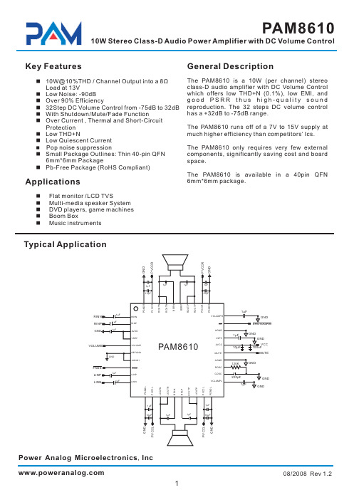
The PAM8610 is a 10W (per channel) stereo class-D audio amplifier with DC Volume Control which offers low THD+N (0.1%), low EMI, and good PSRR thus high-quality sound reproduction. The 32 steps DC volume control has a +32dB to -75dB range.
26
AVCC High-voltage analog power supply (7V to 15V)
2.5V Reference for analog cells, as well as reference for unused audio input
27
V2P5
when using single-ended inputs.
3
08/2008 Rev 1.2
元器件交易网
PAM8610
10W Stereo Class-D Audio Power Amplifier with DC Volume Control
Pin Descriptions
Pin Number Name
The PAM8610 is available in a 40pin QFN 6mm*6mm package.
n Flat monitor /LCD TVS n Multi-media speaker System n DVD players, game machines n Boom Box n Music instruments
5
- 1、下载文档前请自行甄别文档内容的完整性,平台不提供额外的编辑、内容补充、找答案等附加服务。
- 2、"仅部分预览"的文档,不可在线预览部分如存在完整性等问题,可反馈申请退款(可完整预览的文档不适用该条件!)。
- 3、如文档侵犯您的权益,请联系客服反馈,我们会尽快为您处理(人工客服工作时间:9:00-18:30)。
PAM8610
10W Stereo Class-D Audio Power Amplifier with DC Volume Control
Key Features
General Description
n 10W@10%THD / Channel Output into a 8Ω Load at 13V
Protection n Low THD+N n Low Quiescent Current n Pop noise suppression n Small Package Outlines: Thin 40-pin QFN
6mm*6mm Package n Pb-Free Package (RoHS Compliant)
31,40
PGNDR Power ground for right channel H-bridge
32,39
PVCCR Power supply for right channel H-bridge, not connected to PVCCL or AVCC.
33,34
ROUTP Class-D 1/2-H-bridge positive output for right channel
15
BSLN Bootstrap I/O for left channel, negative high-side FET
16
BSLP Bootstrap I/O for left channel, positive high-side FET
17,18
LOUTP Class-D 1/2-H-bridge positive output for left channel
11,20
PGNDL Power ground for left channel H-bridge
12,19
PVCCL Power supply for left channel H-bridge, not connected to PVCCR or AVCC.
13,14
LOUTN Class-D 1/2-H-bridge negative output for left channel
21
VCLAMPL Internally generated voltage supply for left channel bootstrap capacitors.
I/O for charge/discharging currents onto capacitor for ramp generator triangle
3
08/2008 Rev 1.2
元器件交易网
PAM8610
10W Stereo Class-D Audio Power Amplifier with DC Volume Control
Pin Descriptions
Pin Number Name
7
AGND1 Analog GND
Input for controlling volume ramp rate when cycling SD or during power-up. A
8
FADE logic low on this pin places the amplifier in fade mode. A logic high on this pin
ROSC COSC AVDD
SD
V2P5 MUTE
LINN LINP
-+ +-
Gain Adjust
osc
LDO
Biases & References
_ + _
+
PAM Modulation
Driver Driver
Feedback System
on/off Depop
Thermal
Short Circuit Protection
5
VOLUME DC voltage that sets the gain of the amplifier
Ground for gain control circuitry. Connect to AGND. If using a DAC to control the
6
REFGND
volume, connect the DAC ground to this terminal.
The PAM8610 is available in a 40pin QFN 6mm*6mm package.
n Flat monitor /LCD TVS n Multi-media speaker System n DVD players, game machines n Boom Box n Music instruments
Typical Application
GND PVCCR PVCCR GND
1μF
1μF
10μF
1μF
1μF
10μF
PGNDR PVCCR ROUTN ROUTN
BSRN BSRP ROUTP ROUTP PVCCR PGNDR
RINN RINP GND
1μF 1μF 1μF
VOLUME
GND
FADE LINP LINN
allows a quick transition to the desired volume setting.
9
LINP Positive differential audio input for left channel
10
LINN Negative differential audio input for left channel
Power Analog Microelectronics,Inc
2
08/2008 Rev 1.2
元器件交易网
PAM8610
10W Stereo Class-D Audio Power Amplifier with DC Volume Control
-+ +-
_ + _
+
PAM Modulation
Driver Driver
Feedback System
BSRN PVCCR ROUTN PGNDR BSRP PVCCR ROUTP PGNDR
AVCC AGND
BSLN PVCCL LOUTN PGNDL BSLP PVCCL LOUTP PGNDL
26
AVCC High-voltage analog power supply (7V to 15V)
2.5V Reference for analog cells, as well as reference for unused audio input
27
V2P5
when using single-ended inputs.
Applications
The PAM8610 is a 10W (per channel) stereo class-D audio amplifier with DC Volume Control which offers low THD+N (0.1%), low EMI, and good PSRR thus high-quality sound reproduction. The 32 steps DC volume control has a +32dB to -75dB range.
22
COSC
wave biased at V2P5
23
ROSC Current setting resistor for ramp generator. Nominally equal to 1/8*VCC
24,28
AGND Analog GND
25
MUTE A logic high on this pin disables the outputs and a logic low enables the outputs.
Pin Configuration & Marking Information
Top View 6mm*6mm QFN
PGNDR PVCCR ROUTN ROUTN BSRN BSRP ROUTP ROUTP PVCCR PGNDR
RINN
40 39 38 37 36 35 34 33 32 31
1
n Low Noise: -90dB n Over 90% Efficiency n 32Step DC Volume Control from -75dB to 32dB n With Shutdown/Mute/Fade Function n Over Current , Thermal and Short-Circuit
Shutdown signal for IC (low= shutdown, high =operational). TTL logic levels with
29
SD
compliance to VCC.
30
VCLAMPR Internally generated voltage supply for right channel bootstrap capacitors.
The PAM8610 runs off of a 7V to 15V supply at much higher efficiency than competitors’ Ics.
The PAM8610 only requires very few external components, significantly saving cost and board space.