IRS2092应用
IR2092应用

1)对于过流保护设置值问题:电流保护阀值选取:流过FET 的电流包括音频输出和LPF 滤波网络电流,所以;实际要求设置值要高于音频电流峰值。
我比较喜欢这样选取:功放饱和输出时的最大输出电流X1.5;2)RDSON选取:可以根据实际最高工作温度选取,通常可以取85C 时的RDSON 值;3)有了电流和RDSON,就可以选IC 的保护值了。
这里需要注意的是大电流下的FET 开关波型应该是很干净的方波,如果有毛刺的话,可以适当增加栅电阻和优化退耦结构。
对于直流输出问题:可能重载时;电源电压跌落,但;由于变压器或负载正负不对称,正负电源电压跌落不一致,致使功放某一半波提前饱和输出了。
出现这问题时;通常不是功放问题,你可以略微提高电源电压增加水塘电容试试。
2)一般理想的工程条件下,半桥工作的实际死区时间越短越好,最小可以设置到10 纳秒3)IRS2092S 做全频功放时应注意的问题,最好能选择线性度比较好的元件,调制频率选择在300~400KHz,适当匹配LC 滤波器的L/C 的值,可以比较要的解决问题。
推荐L 选取18~22μH。
如果要进一步改善平坦度,L 可以取到10μH,同时;调制频率提高到400KHz 左右。
4)PWM 调制及咔哒声抑制问题:电路的过度过程不匹配,前级电源电压降落引起的电压飘逸被后级放大造成的。
调整一下时续可以解决问题。
另:IRS2092/S 已经在IC 内加入开关机消“咔哒”功能。
一般无需外加电路。
5)针对不同Qg 的MOS,栅电阻怎么选择,Qg 太大2092 发热非常快的解决:可以用降频或增加栅电阻方式降低IRS2092 的温升,一般;Qg 和开关频率并不是IC 发热的主要原因,发热可能更多的源于开关管产生的电压过冲,改善PCB 布线和退耦可以抑制IC 发热。
对于300W 额定输出功率,推荐IRFI4020-117P会更好些。
6)做500W的功放可以用IRS2092 搭配IRF6785MTRPbF 两并,PCB 设计合理的话;THD+N可以达到0.02%以上的水平。
IR-IRS2092-1700W单路D类音频功率放大方案
IR-IRS2092-1700W单路D类音频功率放大方案IR IRS2092 1700W单路D类音频功率放大方案2012-10-30 22:37:47| 分类:默认分类|字号订阅IR公司的 IRS2092是集成了PWM调制器和保护的高压高性能D类音频放大器,工作频率高达800kHz,±100 V额定电压是可提供500W输出功率,主要用在家庭影院,密你立体声系统,通用音频放大器等。
本文介绍IRS2092主要特性,方框图,典型连接图,典型应用电路图以及1700W单路D类音频功率放大器框图,主要特性,电路图和材料清单。
The IRS2092 is a high voltage, high performance Class D audio amplifier driver with PWM modulator and protection.In conjunction with two external MOSFET and a few external components, a complete Class D audio amplifier with protection can be realized.International Rectifier’s proprietary noise isolation technology allows high current gate drive stage and high speed low noise error amplifier reside on a single small silicon die.Open elements of PWM modulator section allow flexible PWM topology implementation.IRS2092主要特性:? Integrated analog input Class D audio amplifier driver in a small 16 pin package? Floating inputs enable easy half bridge implementation? Programmable bidirectional over-current protection with self-reset function? Programmable preset deadtime for improved THD performances? Start and stop click noise reduction? High noise immunity? ±100 V ratings deliver up to 500 W in output power? Operates up to 800 kHz? RoHS compliantIRS2092典型应用:? Home theater systems? Mini component stereo systems? Powered speaker systems? General purpose audio power amplifiers图1。
输出波形可控的高精度数控电源设计

输出波形可控的高精度数控电源设计方案设计系统的总体设计方案如图1所示。
系统工作前在触摸液晶屏上设置电源输出波形、频率以及电压幅值,确定后触摸液晶屏将电源输出参数通过串口通信传递到微处理器,微处理根据设置参数控制信号发生器并经电压幅值调节得到预设模拟信号,最后经过功率放大电路之后驱动负载。
同时,A/D转换电路将负载两端电压以及流经负载的电流进行模/数转换,经微处理器进行数据处理后,在触摸液晶上显示电源当前输出状态。
E2PROM存储默认输出波形类型、幅值和频率的参数值。
图1 电源系统原理框图1.2 直接数字频率合成原理传统的信号发生器采用分立元件以及模拟集成电路,以RC或LC自激振荡为主振级的信号发生器,虽然结构简单,频率范围宽,但是还是克服不了稳定性、准确性差的问题。
石英晶体振荡器虽然稳定度和准确度高,但它的频率不可调,工作场合比较单一。
针对传统信号发生器的缺陷,本设计中采用DDS来产生正弦波。
DDS基本结构包括参考时钟、相位累加器、正弦查询表、D/A转换器和低通滤波器5个部分组成,它是采用高稳定的参考时钟量化抽样时间间隔,利用信号相位与时间成线性关系的特性,直接对所需信号进行抽样、量化和映射,输出频率可调的模拟信号。
2 主要硬件单元设计本设计硬件部分主要由DDS信号发生器电路、电压幅值调节电路和D类功率放大电路等组成。
2.1 DDS信号发生器电路电源输出波形是由信号发生器经电压幅值调节电路和功率放大电路之后得到,所以信号发生器的性能高低是决定其频率精度以及稳定性的重要因素之一。
因此,设计一个高频率精度、稳定性强的信号发生器是保证本电源性能的关键。
本设计采用美国A/D公司的DDS芯片AD9850,通过微处理器程序控制和处理AD9850的32位频率控制字,得到正弦波和方波,再配合积分电路得到三角波以及锯齿波。
AD9850可实现全数字编程控制的频率合成,通过内部高速比较器可直接输出方波。
AD9850的输出频率:[fout=M·fclk232] (1)式中:fclk为时钟频率;M为频率控制字,频率控制字M可表达为fout×[232fclk],所以根据预设的输出频率可以计算出相应的频率控制字。
irs2092s原理

irs2092s原理
IRS2092S 是一种高性能数字功率放大器的集成电路,其原理基于谐振控制技术。
该芯片可处理音频信号,将其转换成高质量的输出功率,可以驱动千瓦级的负载。
IRS2092S 的工作原理是将音频信号转换成数字信号,通过高速的PWM技术将数字信号转换成PWM信号,然后通过谐振电路将PWM信号对负载进行调制,得到高品质,高效率的输出功率。
与传统的功率放大器相比,IRS2092S 具有以下优点:
1.高效率:采用PWM 技术,可实现高效率的功率转换;
2.高保真性:数字信号处理可以保证输出信号的高保真性;
3.灵活性:可按照不同的应用需求进行配置和调整;
4.可靠性:采用先进的保护电路,可以保证芯片和设备的可靠性和稳定性。
IRS2092S 通常应用于家庭影院、公共场所、演出场所等需要高品质声音的场合。
IRS2092S D类功放 pdf

September 2007IRS2092PROTECTED DIGITAL AUDIO AMPLIFIERFeatures•Integrated analog input Class D audio amplifier driver in a small 16 pin package• Floating inputs enable easy half bridgeimplementation• Programmable bidirectional over-currentprotection with self-reset function• Programmable preset deadtime for improvedTHD performances• Start and stop click noise reduction • High noise immunity• ±100 V ratings deliver up to 500 W in outputpower• Operates up to 800 kHz • RoHS compliantTypical Applications• Home theater systems• Mini component stereo systems • Powered speaker systems•General purpose audio power amplifiersProduct SummaryV OFFSET (max)± 100 VIo+ 1.0 AGate driverIo - 1.2 ASelectable Deadtime 25/40/65/105 ns OC protection delay (max) 500 ns DC offset <20 mV PWM frequency ~800 kHz Error amplifier open loop gain >60 dBTHD+N* (1kHz, 50W, 4Ω) 0.01 % Residual Noise*(AES-17 Filter)200 µVrms* measured with recommended circuitPackage OptionsSOIC16N PDIP16Table of Contents Page Description 3 Simplified Block Diagram 4 Typical Application Diagram 4 Qualification Information 5 Absolute Maximum Ratings 6 Recommended Operating Conditions 7 Electrical Characteristics 8 Waveform Definitions 10 Functional Block Diagram 11 Input/Output Pin Equivalent Circuit Diagram 12 Lead Definitions 13 Lead Assignments 13 Package Details 14 Tape and Reel Details 16 Part Marking Information 17 Ordering Information 18DescriptionThe IRS2092 is a high voltage, high performance Class D audio amplifier driver with PWM modulator and protection. In conjunction with two external MOSFET and a few external components, a complete Class D audio amplifier with protection can be realized.International Rectifier’s proprietary noise isolation technology allows high current gate drive stage and high speed low noise error amplifier reside on a single small silicon die.Open elements of PWM modulator section allow flexible PWM topology implementation.ΩRefer to IRAUDAMP5 reference design for details.Qualification Information†Industrial††(per JEDEC JESD 47E)Qualification Level Comments: This IC has passed JEDEC’s Industrialqualification. IR’s Consumer qualification level is grantedby extension of the higher Industrial level.SOIC16N Moisture Sensitivity LevelDIP16MSL3†††(per IPC/JEDEC J-STD-020C)Machine ModelClass B(per JEDEC standard JESD22-A114D)Human Body ModelClass 2(per EIA/JEDEC standard EIA/JESD22-A115-A)ESDCharged Device ModelClass IV(per JEDEC standard JESD22-C101C)IC Latch-Up Test Class I, Level A (per JESD78A)RoHS Compliant Yes†Qualification standards can be found at International Rectifier’s web site /††Higher qualification ratings may be available should the user have such requirements. Please contact your International Rectifier sales representative for further information.†††Higher MSL ratings may be available for the specific package types listed here. Please contact your International Rectifier sales representative for further information.Absolute Maximum RatingsAbsolute Maximum Ratings indicate sustained limits beyond which damage to the device may occur. Allvoltage parameters are absolute voltages referenced to COM; all currents are defined positive into any lead.The Thermal Resistance and Power Dissipation ratings are measured under board mounted and still airconditions.Symbol Definition MinMaxUnits V B High side floating supply voltage -0.3 220V S High side floating supply voltage (Note2) V B -20 V B +0.3V HO High side floating output voltage V S -0.3 V B +0.3V CSH CSH pin input voltage V S -0.3 V B +0.3V CC Low side fixed supply voltage (Note2) -0.3 20V LO Low side output voltage -0.3 Vcc+0.3V AA Floating input positive supply voltage (Note2) (See I AAZ) 210V SS Floating input negative supply voltage (Note2)-1(See I SSZ)GND +0.3V GND Floating input supply ground voltageV SS -0.3(See I SSZ)V AA +0.3(See I AAZ)VI IN-Inverting input current (Note1) --- ±3 mAV CSD SD pin input voltage V SS -0.3 V AA +0.3V COMP COMP pin input voltage V SS -0.3 V AA +0.3V DT DT pin input voltage -0.3 V CC +0.3V OCSET OCSET pin input voltage -0.3 V CC+0.3VI AAZ Floating input positive supply zener clamp current (Note2) --- 20I SSZ Floating input negative supply zener clamp current (Note2) --- 20I CCZ Low side supply zener clamp current (Note3) --- 10I BSZ Floating supply zener clamp current (Note3) --- 10I OREF Reference output current --- 5mAdV S/dt Allowable Vs voltage slew rate --- 50 V/ns dV SS/dt Allowable Vss voltage slew rate (Note3) --- 50 V/msSOIC16N --- 1.0 Pd Maximum power dissipation @ T A ≤ +25°CDIP16 --- 1.6WSOIC16N --- 115 Rth JA Thermal resistance, Junction to ambientDIP16 --- 75°C/W T J Junction Temperature --- 150 °C T S Storage Temperature -55 150 °C T L Lead temperature (soldering, 10 seconds) --- 300 °CNote1:IN- contains clamping diode to GND.Note2: V DD – IN+, GND -V SS, V CC-COM and V B-V S contain internal shunt zener diodes. Please note that the voltage ratings of these can be limited by the clamping current.Note3: For the rising and falling edges of step signal of 10 V. V SS=15 V to 200 V.Recommended Operating ConditionsFor proper operation, the device should be used within the recommended conditions below. The Vs and COM offset ratingsare tested with supplies biased at V AA-V SS=10 V, V CC=12 V and V B-V S=12 V. All voltage parameters are absolute voltagesreferenced to COM; all currents are defined positive into any lead.UnitsMax.Symbol Definition Min.V B High side floating supply absolute voltage V S +10 V S +18V V S High side floating supply offset voltage (Note 1) 200I AAZ Floating input positive supply zener clamp current 1 11mAI SSZ Floating input negative supply zener clamp current 1 11V SS Floating input supply absolute voltage 0 200V HO High side floating output voltage Vs V BV CC Low side fixed supply voltage 10 18V LO Low side output voltage 0 V CCV V GND GND pin input voltage V SS(Note 3)V AA(Note3)V IN-Inverting input voltage V GND -0.5 V GND +0.5V CSD CSD pin input voltage V SS V AAV COMP COMP pin input voltage V SS V AAC COMP COMP pin phase compensation capacitor to GND 1 - nFV DT DT pin input voltage 0 V CC V0.8mAI OREF Reference output current to COM (Note 2) 0.3V OCSET OCSET pin input voltage 0.5 5V V CSH CSH pin input voltage Vs V BdVss/dt Allowable Vss voltage slew rate upon power-up (Note4) - 50 V/msI PW Input pulse width 10 (Note 5) - nsf SW SwitchingFrequency - 800 kHzTemperature -40 125 °C T A AmbientNote 1:Logic operational for Vs equal to –5 V to +200 V. Logic state held for Vs equal to –5 V to –V BS.Note 2: Nominal voltage for V REF is 5.1 V. I OREF of 0.3 – 0.8 mA dictates total external resistor value on VREF to be 6.3 kΩ to16.7 kΩ.Note 3: GND input voltage is limited by I AAZ and I SSZ.Note 4: V SS ramps up from 0 V to 200 V.Note 5: Output logic status may not respond correctly if input pulse width is smaller than the minimum pulse width.Electrical CharacteristicsV CC ,V BS = 12 V, V SS =V S =COM=0 V, V AA =10 V, C L =1 nF and T A =25 °C unless otherwise specified. SymbolDefinition Min Typ Max Units Test ConditionsLow Side SupplyUV CC+ Vcc supply UVLO positive threshold 8.4 8.9 9.4UV CC- Vcc supply UVLO negative threshold 8.2 8.7 9.2UV CCHYS UV CC hysteresis - 0.2 - V I QCC Low side quiescent current - - 3 mA V DT =V CC V CLAMPL Low side zener diode clamp voltage 19.6 20.4 21.6 VI CC =5 mA High Side Floating SupplyUV BS+ High side well UVLO positive threshold 8.0 8.5 9.0UV BS- High side well UVLO negative threshold 7.8 8.3 8.8 UV BSHYS UV BS hysteresis - 0.2 - V I QBS High side quiescent current - - 1 mAI LKH High to Low side leakage current - - 50 µA V B =V S =200 V V CLAMPH High side zener diode clamp voltage 19.6 20.4 21.6 VI BS =5 mAFloating Input SupplyUV AA+ VA+, VA- floating supply UVLO positivethreshold from V SS8.2 8.7 9.2 V SS =0 V, GND pinfloatingUV AA-VA+, VA- floating supply UVLO negative threshold from V SS7.7 8.2 8.7V SS =0 V, GND pinfloatingUV AAHYS UV AA hysteresis - 0.5 -V V SS =0 V, GND pinfloatingI QAA0 Floating Input positive quiescent supply current- 0.5 2V AA =10 V, V SS =0 V,V CSD =VSSI QAA1 Floating Input positive quiescent supply current- 8 11V AA =10 V, V SS =0 V,V CSD =VAAI QAA2 Floating Input positive quiescent supply current- 8 11mA V AA =10 V, V SS =0 V,V CSD =GND I LKM Floating input side to Low side leakage current- - 50 µAV AA =V SS =V GND =100 VV CLAMPM+ V AA floating supply zener diode clamp voltage, positive, with respect to GND 6.0 7.0 8.0I AA =5 mA, I SS =5 mA,V GND =0 V, V CSD =VSSV CLAMPM-V SS floating supply zener diode clamp voltage, negative, with respect to GND -8.0 -7.0 -6.0VI AA =5 mA, I SS =5 mA,V GND =0 V, V CSD =VSS Audio Input (V GND =0, V AA =5V, V SS =-5V)V OS Input offset voltage -15 0 15 mV I BIN Input bias current - - 40 nABWSmall signal bandwidth- 9-MHz C COMP =2 nF, Rf=3.3 k ΩV COMP OTA Output voltage VAA-1 - VSS+1Vg m OTA transconductance - 100 - mS V IN-=10 mVG V OTA gain 60 - - dB V NrmsOTA input noise voltage- 250 - mVrms BW=20 kHz, Resolution BW=22 Hz Fig.5 SR Slew rate - ±5 - V/us C COMP =1 nFCMRR Common-mode rejection ratio - 60 - PSRR Supply voltage rejection ratio-65-dBPWM comparatorVth PWM PWM comparator threshold in COMP - (V AA -V SS )/2 - V f OTACOMP pin star-up local oscillation 0.7 1.0 1.3 MHz V CSD =GNDfrequencyProtectionV REF Reference output voltage 4.8 5.1 5.4 I OREF =0.5 mAVth OCL Low side OC threshold in Vs 1.1 1.2 1.3OCSET=1.2 V,Fig.6Vth OCH High side OC threshold in V CSH 1.1+ Vs 1.2+ Vs 1.3+ Vs Vs=200 V, Vth1 CSD pin shutdown release threshold 0.62xV DD 0.70xV DD 0.78xV DD Vth2 CSD pin self reset threshold 0.26xV DD 0.30xV DD 0.34xV DD VI CSD+ CSD pin discharge current 70 100 130 V CSD = V SS +5 VI CSD- CSD pin charge current 70 100 130 µAV CSD = V SS +5 V t SD Shutdown propagation delay from V CSD >V SS + Vth OCH to Shutdown- - 250t OCH Propagation delay time from V CSH >Vth OCH to Shutdown- - 500 Fig.3t OCL Propagation delay time from Vs> Vth OCLto Shutdown- - 500 ns Fig.4Gate DriverIo+ Output high short circuit current (Source) - 1.0 - A Vo=0 V, PW<10 µs Io- Output low short circuit current (Sink) - 1.2 - A Vo=12 V, PW<10 µsV OL Low level out put voltageLO – COM, HO - VS- - 0.1V OH High level out put voltageVCC – LO, VB - HO- - 1.4V Io =0 Aton High and low side turn-on propagation delay- 360 -V DT = V CCtoff High and low side turn-off propagation delay- 335 -V DT = V CCtr Turn-on rise time - 20 50 tf Turn-off fall time - 15 35 DT1 Deadtime: LO turn-off to HO turn-on(DT LO-HO ) & HO turn-off to LO turn-on (DT HO-LO )15 25 35V DT >V DT1,DT2 Deadtime: LO turn-off to HO turn-on(DT LO-HO ) & HO turn-off to LO turn-on (DT HO-LO )25 40 55V DT1>V DT > V DT2,DT3 Deadtime: LO turn-off to HO turn-on(DT LO-HO ) & HO turn-off to LO turn-on (DT HO-LO )50 65 85V DT2>V DT > V DT3,DT4 Deadtime: LO turn-off to HO turn-on(DT LO-HO ) & HO turn-off to LO turn-on (DT HO-LO )V DT = V DT485 105 135nsV DT3>V DT > V DT4,V DT1 DT mode select threshold 2 0.51xVcc 0.57xVcc 0.63xVcc V DT2 DT mode select threshold 3 0.32xVcc 0.36xVcc 0.40xVcc V DT3DT mode select threshold 4 0.21xVcc 0.23xVcc 0.25xVcc VWaveform DefinitionsVth1t SD90%CSDHO/LOFigure 1: Switching Time Waveform Definitions Figure 2: CSD to Shutdown Waveform DefinitionsVth OCLt OCL90%VSLOVth OCHt OCH90%CSHHOVSFigure 3: V S > Vth OCL to Shutdown Waveform Figure 4: V CSH > Vth OCH to Shutdown WaveformFigure 5: OTA input noise voltage mesurent circuitLOW SIDE CSLead Definitions: IRS2092Pin # Symbol Description1 VAA Floating input positive supply2 GND Floating input supply return3 IN- Analog inverting input4 COMP Phase compensation input, comparator input5 CSD Shutdown timing capacitor6 VSS Floating input negative supply7 VREF 5V reference voltage to program OCSET pin 8 OCSET Low side over current threshold setting 9 DT Deadtime program input 10 COM Low side supply return 11 LO Low side output 12 VCC Low side supply13 VS High side floating supply return 14 HO High side output15 VB High side floating supply16 CSHHigh side over current sensing inputLead AssignmentsVAA GND IN-OCSETCOM COMP CSD LO VCC VREF HO VS VSS CSH VB DTPDIP16 and SOIC16NPackage Details: PDIP16Package Details: SOIC16NTape and Reel Details: SOIC16NCPart Marking InformationOrdering InformationStandard PackBase Part NumberPackage TypeForm QuantityComplete Part NumberPDIP16 Tube/Bulk 25IRS2092PBF Tube/Bulk 45 IRS2092SPBF IRS2092SOIC16NTape and Reel2500IRS2092STRPBFThe information provided in this document is believed to be accurate and reliable. However, International Rectifier assumes no responsibility for the consequences of the use of this information. International Rectifier assumes no responsibility for any infringement of patents or of other rights of third parties which may result from the use of this information. No license is granted by implication or otherwise under any patent or patent rights of International Rectifier. The specifications mentioned in this document are subject to change without notice. This documentsupersedes and replaces all information previously supplied.For technical support, please contact IR’s Technical Assistance Center/technical-info/WORLD HEADQUARTERS:233 Kansas St., El Segundo, California 90245Tel: (310) 252-7105。
二氧化碳传感器 分类 应用场景 工作原理

二氧化碳传感器分类应用场景工作原理下载提示:该文档是本店铺精心编制而成的,希望大家下载后,能够帮助大家解决实际问题。
文档下载后可定制修改,请根据实际需要进行调整和使用,谢谢!本店铺为大家提供各种类型的实用资料,如教育随笔、日记赏析、句子摘抄、古诗大全、经典美文、话题作文、工作总结、词语解析、文案摘录、其他资料等等,想了解不同资料格式和写法,敬请关注!Download tips: This document is carefully compiled by this editor. I hope that after you download it, it can help you solve practical problems. The document can be customized and modified after downloading, please adjust and use it according to actual needs, thank you! In addition, this shop provides you with various types of practical materials, such as educational essays, diary appreciation, sentence excerpts, ancient poems, classic articles, topic composition, work summary, word parsing, copy excerpts, other materials and so on, want to know different data formats and writing methods, please pay attention!二氧化碳传感器:探索未来环境监测的利器引言在当今社会,环境污染日益严重,特别是空气质量的恶化引起了人们的广泛关注。
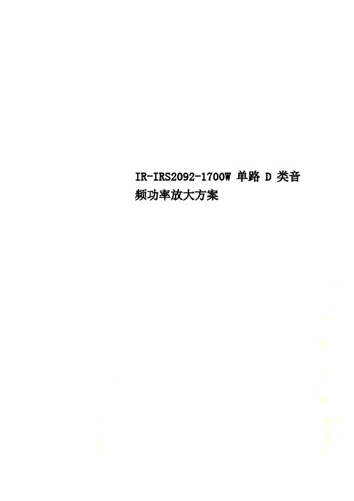
基于IRS2092驱动器IC的D类音频功率放大器
可 知 , 死 区 时 间 为 4 n :再 如 ,若 选 取 电流 检测在 引脚 C H 内部 有一个 固定 在 D 5s S 4是 必要的。扣除 D 4约 06 . V的正 向压
音 频 功 率 放 大 器 , 输 出 功 率 范 围 为
一
△P WM 调制器 、 电平移位 器、 区时 死
基本 应用 电路
基 于 IS 0 2和 数 字 音 频 双 功 率 R29
2 — 0 W ,总谐波失真加噪 声( H N) 间及 OC 5 50 T D+ P和 U P电路、 / V 高 低端 MOS —
2 区时间选择 IS 0 2 . 死 R 2 9 中高、 低端 U1引脚 H O和 L 上 的输 出驱 动器 高 / 驱动信号 之间的死区时间取决于 引脚 D O T S E ,并确 保两 个 MOS 上 的电压 V 如图 3所示。而 V — IS 0 2采 用 1 引脚 无铅 封 装 ( R 29 6 引 低 端功率 MO F T , 甜又取决
R2 6 8 6= . k0 , 7 3 9 R2 = . kO , V O 36 c, . Vc
・
新器 件应 用 ・
基 于 I 29 RS 0 2驱 动 器 I 的 D 类 音 频 c 功率放大器
藏取光 利 用美 国国际 整流 器公 司 的数字 音 音 频 放 大 器 的 高 压 ( 达 2 0 直 0 V) 高 速 大 了 的 P M 波 形 ,经 L 和 O1 成 的 W 1 2组 频 驱 动 器 IS 0 2和 数 字 音 频 双 功 率 MOS E R29 F T驱动器 I。 IS 0 2含 有输入 低通滤波器 ( P ) C R 29 L F 滤波还原 为模拟音频信 MOS E , F T 可以设计单通道 或两通道 D类 运 算 放 大 器 、 模 拟 输 入 自振 荡 二 阶 号 驱 动 扬 声器 。
ISR2092S-评估板设计-iraudamp7s

IRAUDAMP7S REV 1.3
Page 1 of 42
Item
Table of Contents
Page
1
Introduction of scalable design ………………………………………………….. 3
2
Power table values for each power model……………………………………… 4
±70V
±60V ~ ±80V
40
Notes:
• All the power ratings are at clipping power (THD+N = 1 %). To estimate power ratings at THD+N=10%, multiply them by 1.33
• See Table 5 on page 36 for the complete listing of components table.
IRAUDAMP7S REV 1.3
Page 2 of 42
Introduction
The IRAUDAMP7S reference design is a two-channel Class D audio power amplifier that features output power scalability. The IRAUDAMP7S offers selectable half-bridge (stereo) and full-bridge (bridged) modes.
7
Clipping characteristics…………………………………………………………… 14
- 1、下载文档前请自行甄别文档内容的完整性,平台不提供额外的编辑、内容补充、找答案等附加服务。
- 2、"仅部分预览"的文档,不可在线预览部分如存在完整性等问题,可反馈申请退款(可完整预览的文档不适用该条件!)。
- 3、如文档侵犯您的权益,请联系客服反馈,我们会尽快为您处理(人工客服工作时间:9:00-18:30)。
IR IRS2092 D类240瓦放大器方案关键词:消费类电子,音频放大器,D类放大器,MOSFET,摘要:IR 公司的IRAUDAMP5 D类240瓦音频3率放大器方案采用IRS2092S D 类音频控制器和栅极驱动器和IRF6645 DirectFET MOSFET。
參考设计在1/8连续额定功率时不需要散热器,两路设计对于输出功率和路数可配置,广泛应用在AV接收器,家庭影院系统,大功率杨声器,低音喇叭,乐器放大器以及汽车电子放大器。
本文介绍了IRS2092S 和IRAUDAMP5參考设计的主要性能,方框图以及參考设计的多种应用电路。
IR 公司的IRAUDAMP5 D类240瓦音频3率放大器方案采用IRS2092S D 类音频控制器和栅极驱动器和IRF6645 DirectFET MOSFET。
參考设计在1/8连续额定功率时不需要散热器,两路设计对于输出功率和路数可配置,广泛应用在AV接收器,家庭影院系统,大功率杨声器,低音喇叭,乐器放大器以及汽车电子放大器。
本文介绍了IRS2092S和IRAUDAMP5參考设计的主要性能,方框图以及參考设计的多种应用电路。
IRS2092 PROTECTED DIGITAL AUDIO AMPLIFIER主要特性:• Integrated analog input Class D audio amplifier driver in a small 16 pin package• Floating inputs enable easy half bridge implementation• Programmable bidirectional over-current protection with self-reset function• Programmable preset deadtime for improved THD performances• Start and stop click noise reduction• High noise immunity• ±100 V ratings deliver up to 500 W in output power• Operates up to 800 kHz• RoHS compliant典型应用:• Home theater systems• Mini component stereo systems• Powered speaker systems• General purpose audio power amplifiers图1. IRS2092方框图图2.IRS2092典型应用电路图IRAUDAMP5120W x 2 Channel Class D Audio Power Amplifier Using the IRS2092S and IRF6645图3. IRAUDAMP5參考设计外形图(两路120W半桥D类音频放大器)Two-channel 120 W Half-bridge Class-D Audio Power AmplifierThe IRAUDAMP5 reference design is a two-channel, 120W half-bridge Class D audio power amplifier. This reference design demonstrates how to use the IRS2092S Class D audio controller and gate driver IC, implement protection circuits, and design an optimum PCB layout using the IRF6645 DirectFET MOSFETs. The resulting design requires no heatsink for normal operation (one-eighth of continuous rated power). The reference design provides all the required housekeeping power supplies for ease of use. The two-channel design is scalable for power and the number of channels.应用:AV receiversHome theater systemsMini component stereosPowered speakersSub-woofersMusical Instrument amplifiersAutomotive after market amplifiers主要特性:Output Power: 120W x 2 channels,Total Harmonic Distortion (THD+N) = 1%, 1 kHzResidual Noise: 170μV, IHF-A weighted, AES-17 filterDistortion: 0.005% THD+N @ 60W, 4ΩEfficiency: 96% @ 120W, 4Ω, single-channel driven, Class D stageMultiple Protection Features: Over-current protection (OCP), high side and low sideOver-voltage protection (OVP),Under-voltage protection (UVP), high side and low sideDC-protection (DCP),Over-temperature protection (OTP)PWM Modulator: Self-oscillating half-bridge topology with optional clock synchronization主要指标:General Test Conditions (unless otherwise noted) Notes / ConditionsSupply Voltage ±35VLoad Impedance 8-4ΩSelf-Oscillating Frequency 400kHz No input signal, AdjustableGain Setting 26dB 1Vrms input yields rated power Electrical Data Typical Notes / ConditionsIR Devices Used IRS2092S Audio Controller and Gate-Driver,IRF6645 DirectFET MOSFETsModulator Self-oscillating, second order sigma-deltamodulation, analog inputPower Supply Range ± 25V to ±35V Bipolar power supplyOutput Power CH1-2: (1%THD+N)120W 1kHzOutput Power CH1-2: (10%THD+N)170W 1kHzRated Load Impedance 8-4ΩResistive loadStandby Supply Current ±100mA No input signalTotal Idle PowerConsumption7W No input signalChannel Efficiency 96% Single-channel driven,120W, Class D stage .Audio Performance *BeforeDemodulator Class DOutputNotes /ConditionsTHD+N, 1W THD+N, 10W THD+N, 60W THD+N, 100W 0.009%0.003%0.003%0.008%0.01%0.004%0.005%0.010%1kHz, Single-channel drivenDynamic Range 101dB 101dB A-weighted,AES-17 filter,Single-channeloperationResidual Noise, 22Hz - 20kHzAES17 170μV 170μV Self-oscillating –400kHzDamping Factor 2000 170 1kHz, relative to4Ω loadChannel Separation 95dB85dB75dB 90dB80dB65dB100Hz1kHz10kHzFrequency Response : 20Hz-20kHz:20H N/A ±1dB±3dB1W, 4Ω - 8ΩLoadz-35kHzThermal Performance Typical Notes / Conditions Idling T C =30°CT PCB=37°CNo signal input, T A=25°C2ch x 15W (1/8 rated power) T C =54°CT PCB=67°CContinuous, T A=25°C2ch x 120W (Rated power) T C =80°CT PCB=106°C At OTP shutdown @ 150 sec, T A=25°CPhysical SpecificationsDimensions 5.8”(L) x 5.2”(W)图4. IRAUDAMP5 D类放大器简化方框图The IRAUDAMP5 uses the IRS2092S, a high-voltage (up to 200V), high-speed power MOSFET PWM generator and gate driver with internal dead-time and protection functions specifically designed for Class D audio amplifier applications. These functions include OCP and UVP. Bi-directional current protection for both the high-side and low-side MOSFETs are internal to the IRS2092S, and the trip levels for both MOSFETs can be set independently. In this design, the dead time can be selected for optimized performance by minimizing dead time while preventing shoot-through. As a result, there is no gate-timing adjustment on the board. Selectable dead time through the DT pin voltage is an easy and reliable function which requires only two external resistors 。